Active Power Sharing in
Input-Series-Input-Parallel Output-Series
Connected DC/DC Converters
Yiqing Lian, G.P.Adam, D. Holliday, S.J.Finney
Department of Electronic and Electrical EngineeringUniversity of Strathclyde Glasgow, UK Yiqing.lian@strath.ac.uk
Abstract—A high-capacity DC/DC converter with novel input-series-input-parallel output-series connection and with autonomous power sharing between modules is proposed. The proposed scheme is well suited for large-scale wind farm DC collection networks, as it avoids the charging current issues associated with its AC counterpart, and offers lower losses and reduced size and weight when a medium- or high-frequency transformer is used. Small-signal analysis is used to derive the control structures for the converter input and output stages. The proposed control scheme is validated through simulation and experimentation, including demonstration of autonomous power sharing between modules under several operating conditions.
Keywords—DC/DC converter, ISIPOS connection, Power sharing
I. INTRODUCTION
Large offshore wind farms require substantial sub-sea power network to provide internal interconnection. Present solutions are based around conventional medium-voltage AC architectures. Recent studies have highlighted the potential benefits of DC collection networks. Such DC architectures depend on DC/DC conversion to step up the wind-generator output to a voltage compatible with efficient interconnection. Achieving DC/DC conversion at the required voltage and power levels presents a significant challenge for wind-turbine generator’s power electronics. Since voltage levels in medium- and high-voltage systems exceed individual semiconductor device voltage ratings, high-capacity converters often require series connection of power devices.
In this paper, a high-power modular structure DC/DC converter which is realized by input-series-input-parallel output-series (ISIPOS) connection of modules is proposed. Parallel-series architectures can be classified into four categories based on their connection. These categories are input parallel output parallel (IPOP), input parallel output series (IPOS), input series output parallel (ISOP) and input series output series (ISOS) [1]. Currently, the open literature contains no publication in the field of the ISIPOS converter and its control strategy. This structure enables generation of high output voltage with reduced voltage and current stresses at the input side. Moreover, the use of high-frequency (HF)
or medium-frequency (MF) for galvanic isolation [2, 3], allows the heavy line-frequency transformer in an AC grid to be eliminated, leading to significant weight and size savings and much less investment in copper and core material. For example, the estimated mass of a 1MVA medium-frequency (4kHz) transformer is 150kg, whereas that of a 1MVA 50Hz transformer is 3 tons [4]. With series-output connection, the turns-ratio of the isolation transformer can be reduced, leading to a reduction in leakage inductance. Additionally, modular DC/DC converters offer more compact and lighter designs in situations where a single high-voltage converter with series connection of switches can be replaced with a set of low-voltage converter modules as being discussed in this paper. It will also solve the problem of additional snubber component and more complex gate drive units caused by the series connection of switches [5]. Compared to DC/DC converter based modular multilevel converter (MMC), re-configurability and potential for interleaved control may make the ISIPOS DC/DC converter an attractive choice in medium-voltage applications. ISIPOS connection of multiple low-voltage modules provides an excellent solution for scalability of DC/DC converters, with improved robustness and possibility of fault-tolerant operation. Modular architectures offer further advantages, including internal fault management and module reconfiguration as a result of ‘n+k’ designed redundancy and the use of power electronic
[image:1.595.366.521.530.693.2]building blocks (PEBB) to reduce production [6-8].
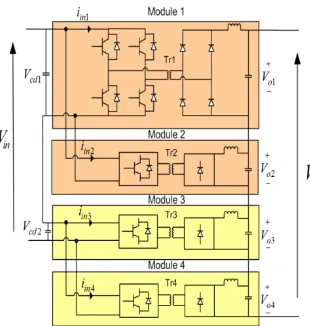
Fig. 1. Four-module ISIPOS DC/DC converter The authors gratefully acknowledge the support of the EPSRC Centre for
Fig.1 shows an illustrative schematic diagram of four-module ISIPOS DC/DC converter that forms the basis of the study. Reliable operation of the ISIPOS modular DC/DC converter requires a control mechanism that ensures equal power sharing among the individual modules, with ability to compensate for any mismatch in the passive components and active switching devices. In this paper, an active input side control scheme for converter power sharing is addressed. Also, the linearized control scheme offered by the Lyapunov control law is applied to provide an improved transient response.
The paper is organized as follows: power sharing in the ISIPOS DC/DC converter is presented in Section 2. In Section 3, the power sharing control strategy for this topology is discussed and the small-signal analyses necessary for controller design are presented. Section 4 presents the simulation and experimental results, and the conclusions are presented in Section 5.
II. POWER SHARING
Assuming all four modules in Fig.1 are lossless, the relationships between the input and output powers of each module can be expressed as (1):
1 1 1
1 2 2
2 3 3
2 4 4
cd in o o cd in o o cd in o o cd in o o
V I V I
V I V I
V I V I
V I V I
(1)
where Vcd1 is the DC input voltage for Modules 1 and 2 due to the parallel connection; Vcd2 is similarly the DC input voltage for Modules 3 and 4; Iin1, Iin2,…,Iin4 are the input currents to Modules 1 to 4, Vo1,Vo2,…,Vo4 are the output voltages from Modules 1 to 4; and Io is the load current. In
steady-state condition, the average filter capacitor current is zero, and therefore only a very small filter inductor current ripple is assumed. If output voltage sharing (OVS) is achieved, then Vo1=Vo2=Vo3=Vo4. Substituting this result into (1) yields (2):
1 1 1 2 2 3 2 4
cd in cd in cd in cd in
V I V I V I V I (2)
Since Iin1=Iin3 due to the series connection, (2) leads to
Iin1=Iin3=Iin2=Iin4and Vcd1=Vcd2. It should be noted that input power balancing can be achieved as long as OVS is achieved. Alternatively, if all modules share the same input power, which means Modules 1 and 2 (similarly for Modules 3 and 4) share the same input current and Modules 1 and 3 share the same input voltage, output voltage sharing is achieved.
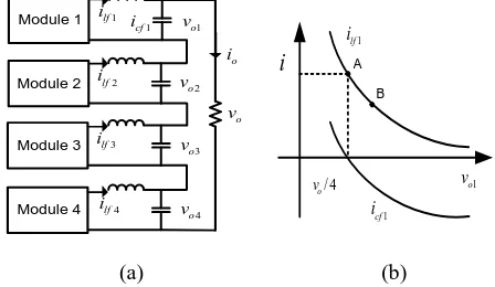
The common feature revealed for an ISOS system [8-11] is the indispensability of input voltage sharing control. Fig.2 (a) illustrates the equivalent schematic diagram of the output side control strategies for the ISIPOS DC/DC converter. Assuming that OVS is achieved through output side control, modules behave as a constant power sink seen from the input side, with constant output current and equally shared output voltages. Thus, any increase of Vcd1 leads to a decrease of icin1 and drives the system from equilibrium
operating point A to B, as shown in Fig.2 (b). Fig.2 (b) also shows that icin1at point B is smaller than input current iin and
that input filter capacitor current icd1 becomes positive, which will further increase Vin1. Thus, the equilibrium point cannot be resumed. An increase in input voltage Vin1 leads to further increase of itself, eventually leading to a runaway condition between Vin1 and Vin2. This means that any input disturbance may result in an inversely proportional current-voltage relationship. OVS cannot therefore provide input power sharing for the ISIPOS system.
Fig.3 (a) and (b) highlight the consequences of input side control. Modules behave as constant power source seen from the output side, with equally shared input voltage and current. Thus, an increase in Vo1 leads to a decrease in ilf1 which drives the system from the equilibrium operating point A to B, as shown in Fig.3 (b). Now, ilf1 is smaller than the load current io, current icf1 becomes negative, discharging the capacitor and driving the operating point back to A. Therefore, a dedicated input control loop is indispensable for ISIPOS DC/DC converter stable operation.
in
v
in
i
Module 1
Module 2
Module 3
Module 4
1
in
i
2
in
i 1
c d
i
2
cd
i 1
cin
i
2
cin
i 1
cd
v
2
cd
v
[image:2.595.317.549.294.398.2](a) (b)
Fig. 2. ISIPOS DC/DC converter (a) output side control and (b) operating point
Module 1
o
i 1
lf
i
1
o
v
2
o
v
Module 2
Module 3
Module 4 2
lf
i
3
lf
i
4
lf
i
3
o
v
4
o
v
o
v 1
cf
i
1
lf
i
A B
1
o
v / 4
o
v
i
1
cf
i
(a) (b)
Fig. 3. ISIPOS DC/DC converter (a) input side control and (b) operating point
III. CONTROLLER DESIGN
Converter output voltage control is normally achieved by a linear control technique such as PI control. In comparison, some non-linear techniques can provide improved transient response which is robust to load, input and parameter variations [12]. Most of the non-linear control laws are complex, which makes them difficult to apply, but the linearization schemes have the advantage of reducing the converter model to an equivalent output filter model which
in
i A
B
1
cd
i
1
in
v 1
cin
i
/ 2
in
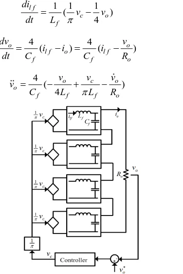
[image:2.595.323.547.442.572.2]significantly simplifies the control design process, without significant compromise to its robustness. A novel linearized equivalent model of the ISIPOS DC/DC converter incorporating closed-loop output voltage control is presented in Fig.4 [13] which provides a linear representation of converter behavior under large-signal variation which is suitable for faster control response and estimation of the converter state variables. This study applies a large signal Lyapunov controller, with the objective of controlling output voltage error for the ISIPOS DC/DC converter:
o o
evv (3)
The first order Lyapunov control function v(x) and its derivative are given in (4) and (5), where α is a proportionality constant and β is strictly a positive proportionality constant [13]:
2
1
( )
2
v ee (3)
( )( ) 0
v e e ee v (4)
1
( ) ( )
2
ee ee (5)
From Fig.4, (6) and (7) can be derived. Control variable
vc can then be explicitly included in the second order transfer
function of the output voltage (8).
1 1 1
( )
4
l f
c o f
di
v v
dt L (6)
4 4
( ) ( )
o o
l f o l f
f f o
dv v
i i i
dt C C R (7)
4
( )
4
o c o o
f f f o
v v v
v
C L
L R (8)
[image:3.595.319.559.55.120.2]
Fig. 4. Simplified large signal control for ISIPOS DC/DC converter Assuming voto be constant, e voand e vo. Based on Fig.4, (9) is deduced. This, in turn, yields (10).
4
( ) ( )
2 2 4
c o o o o o o o
f f f o
v v v
v v v v v
C L L R
(9)
1
( )
8 4 2 4
f f f f
c o
o f
C L C L
v e e v
R C
(10)
The first and second terms of (10) represent a PD controller, where ‘e’ will decay to 0 as the system output
voltage vo converges to its reference value. πvo/4 is a feed-forward term to speed start-up and to help stabilise the controller. Therefore, (10) can be rewritten as (11):
4
c p d o
v k ek e v (11)
The transfer function between the output voltage and the adjusted output from the load voltage controller can be obtained from Fig.4 and expressed as (12):
2
4 1
1
oc
f f
G
L C s
(12)
The resulting closed-loop Lyapunov output voltage controller is shown in Fig.5. The Routh-Hurwitz stability criterion shows that if proportional and derivative gains kp
and kd are both positive, the system is stable. Thus, by
[image:3.595.78.266.362.643.2]designing the damping ratio and natural frequency from the system characteristic equation, the required closed-loop performance can be achieved.
Fig. 5. Lyapunov closed-loop controller
Fig. 6. ISIPOS converter small signal model
- + - +
- + - +
in
v
in
i
1
in
i
2
in
i
1
: 1
k De
2
: 1
k De
1 1
1
( )
in i V d dv
k
1 1
2in o V d k R
1 1
in V d
k
2 2
in V d
k
2 2
2
( )
in i V d dv
k
1 2
1
2in( i v)
o
V d d
k R
2 2
2
2in( i v)
o
V d d
k R
2 2
2in o
V d k R
1
f
L
2
f
L 1
f
C
2
f
C 1
Lf
i
2
Lf
i
1
o
v
2
o
v
o
i
o
R o
v
- + - +
- + - + 4
in
i
3
1:De
k
4
1:De
k
3 3
3
( )
in i V d dv
k
3 3 2in
o
V d k R
3 3
in V d
k
4 4
in V d
k
4 4
4
( )
in i V d dv
k
3 3
3
2in( i v)
o
V d d
k R
4 4
4
2in( i v)
o
V d d
k R
4
4
2in
o
V d k R
3
f
L
4
f
L
3
f
C
4
f
C
3
Lf
i
4
Lf
i
3
o
v
4
o
v
3
in
i
2
d
C
1
d
C
1
cd
v
2
cd
v
[image:3.595.328.557.380.699.2]The small signal model of four ISIPOS connected DC/DC modules is shown in Fig.6 [7], where k1, k2, k3, k4 are transformer turns ratios, Lr is the transformer leakage
inductance, De is the effective duty ratio per module [7], Lf1, Lf2, Lf3, Lf4, Cf1, Cf2, Cf3 andCf4are filter inductances and capacitances for the four modules. Input voltage perturbation is represented by ∆vin, input voltage perturbation components
for Modules 1 and 2, and for Modules 3 and 4 are ∆vcd1 and
∆vcd2 respectively, input current perturbations for the four modules are ∆iin1,∆iin2,∆iin3 and ∆iin4 respectively, and filter inductor current and capacitor voltage perturbations are represented by ∆ilf1,∆ilf2,∆ilf3, ∆ilf4, and ∆vo1,∆vo2,∆vo3 and
∆vo4 respectively. ∆d1,∆d2, ∆d3 and ∆d4are the duty ratio perturbations, and ∆dv1, ∆dv2,∆dv3,∆dv4,∆di1,∆di2, ∆di3, and
∆di4 respectively represent perturbations of the duty ratio due to the input voltage and output current, and are defined in (13) [7].
1 2 2 1
3 4 2 2
32
32
8
r e s
v v cd
in o
r e s
v v cd
in o
r s
ij lfj
in
L D f
d d v
k V R L D f
d d v
k V R L f d i kV (13)
It is assumed that four modules have the same effective duty ratio, transformer turns ratios, and capacitor and inductor values. From Fig.6, equations (14-16) are obtained:
1 1 1 1 2 2 2 3 3 21 1 1
2
4 3
2 2
3 3 3
4 4 4
V L 2 V L 2 V L 2 V L 2 cd
l f o cd
l f o cd
l f o cd
l f
e in
v i f
e in
v i f
e in
v i f
e in
v i f o
D
d d d s
k k
D
d d d s
k k
D
d d d s
k v i v v i v v i v v k D
d d d s
k k i v
(14) 1 1 2 2 3 3 4 4 o
l f f o o
o
l f f o o
o
l f f o o
o
l f f o o
o
o
o
o
v
i sC v i
v
i sC v i
v
i sC v i
v
i sC v
R R R R i (15)
Considering the series pair Modules 1 and 3,
1 1 1 1
3 3 3
1 3 3 ( ) ( ) 2 2
in d d v i
e o
in d d v i
e o
in
l f
in
l f
i sC v d d d
D kR
i sC v d d
v k
i
v
D kR d i
k (16)
Based on (16), neglecting duty ratio perturbations due to input voltage and output current, subtraction of the two equations leads to (17). Subtraction of the first and third equations of (14) leads to (18), and from (15) the modular voltage and current relationship can be obtained as (19):
2 1 3 1 3 1 2( cd cd )
in d e
o
l f l f
sC D d d kR k v v v i i (17)
3 1
2 1
3 1 3 1
(
V 2
L )
( cd cd )
l f l f o
e in
o f
D
d d
k v k
i i v
s v v (18)
1 2 3 4
1 1
1 2 3 4
2 2
1 2 3 4
3 3
1 2 3 4
4 4 1 1 1 1 f o f o f
o o o o
o l f
o o o o
o l f
o o o o
o l f
o o o o
o
o l f
o
f
v v v v
v i
v v v v
v i
v v v v
v i
v v v
sC R sC R sC R s v v R i C (19)
Rearranging (19), the relationship between modular voltage output and inductor current can be represented as (20):
1 1 1 2 2 3 4
2 1 2 2 1 3 4
3 1 3 2 1 2 4
4 1 4 2 1 2 3
o l f l f l f l f
o l f l f l f l f
o l f l f l f l f
o l f l f l f l f
v g i g i i i
v g i g i i i
v g i g i i i
v g i g i i i
(20) where, 1 2 3 ( ) 4 1 4 ( ) o f o f o R g sC R g sC R (21)
Substituting (21) into (18) yields (22):
2 1
1 2 3 1 3
1 1 3 V ( ) 2
( L )( )
cd cd
l f l f o o
e in
f
D
d d
v v
g g i i v v
k k s (22)
Substituting (22) into (21) yields (23):
2 1 1 3 1 1 2 2 2V V
( + + L ) 2
( L + )
in in f o e f c e cd d
g g s
kR k
D
d d
sCd s g
v g k k D v
(23)
1
1 3
2 + ( )( )
cd cd
v v A s d d
(24)
where,
2 1
1 2
2V V
( + + L )+
2 ( )
( L + )
in in f o e f e
g g s
kR k
A s D
sCd g s g
k k D (25)
Assuming that ∆vin=0, and ∆vcd1=-∆vcd2, the relationship between input capacitor voltage and duty ratio is obtained as (26): 1 1 2 3 ( ) ( ) 2 2 ( ) ( ) 2 2 cd cd
A s A s
v d
v A s A s d
(26)
The relationship between input current and duty ratio shown in (27) can be obtained by using a similar procedure.
1 1 2 2 ( ) ( ) 2 2 ( ) ( ) 2 2 in in
B s B s
i d
i B s B s d
3 3 4 4 ( ) ( ) 2 2 ( ) ( ) 2 2 in in
B s B s
i d
i B s B s d
(27) where, 3 4 2V
( ) ( in )
e o
B s D g g
R
3
4
2 ( )( 3 )
( )( 3 )
ac bc
g
a b a b
bc g
a b a b
2 3 4 4 1 4 2
o r s f
f o f
f o f in
R L f
a sL
sC R sC k
b
sC R sC
V c k (28)
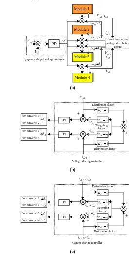
The input-series connection requires input voltage balanced while the input-parallel connection requires input current balance. Individual module input voltages and currents are sensed, and average sharing is used to produce correcting error signals to ensure input power sharing.
As shown in Fig.7, the proposed scheme consists of three loops to ensure input voltage and current sharing among the modules. The Lyapunov controller accordingly contributes the main duty ratio signal ∆d to all modules, which is then
modified by the input current and voltage sharing loops. Average voltage sharing between the two series-connected modules is implemented by correcting the voltage difference signals to generate the duty cycle contributions ∆dv1 and ∆dv2 based on (26).
1 cd V -o V
+ ref V PDLyapunov Output voltage controller
Input current and voltage distribution control
Module 2 Module 1 Module 3 Module 4 1 i n i 2 i n i 4 i n i 2 cd V 3 i n i 1 v d d 1 i d 2 i d 1 v d 2 v d 2 v d 3 i d 4 i d (a)For converter 3:
For converter 4: For converter 1:
For converter 2:
1 1 v Distribution factor Distribution factor
Weighting factor 1 1 2 v w 3 1 v 1 3 2 v w
+ + 1 cd v 1 cd v 2 cd v 2 cd vVoltage sharing controller PI PI 1 v d 2 v d + -+ (b)
For converter 2: For converter 4: For converter 1: For converter 3:
1 1 v Distribution factor Distribution factor
Weighting factor 1 1 2 v w 3 1 v 1 3 2 v w
+ +Current sharing controller PI PI + -+ 1 i d 1 3 in in
i or i
2 4
in in
i or i
1 3
in in
i or i
2 4
in in
i ori
[image:5.595.288.553.107.629.2]3 i d 2 i d 4 i d (c)
Fig. 7. Three-loop control for ISIPOS DC/DC converter (a) output voltage loop structure (b) voltage sharing controller (c) current sharing controller
Master-slave active sharing could also be used, but this is not discussed here. The voltage reference for Modules 1 and 3 is therefore given by (29):
1 2
2
cd cd ref
v v
v (29)
Alternatively, a fixed voltage reference of vin /2 could be
used. The main advantages of using the dynamic input voltage reference in (29) rather than a fixed voltage reference are that it minimizes the interaction among the different control loops and results in better transient performance [1]. Referring to Fig.7, taking Module 1 as an example, the duty ratio contribution of the voltage sharing loop is:
1 ( 1 1) ( 1 1)
v p cd cd i cd cd
d k v v k v v
(30)
The current sharing loop corrects differences in input current between the parallel-connected modules, i.e. Modules 1 and 2, and Modules 3 and 4. Similar to the voltage sharing loop, dynamic current sharing is applied to generate the other duty ratio components ∆di1, ∆di2, ∆di3and
∆di4based on (27). Due to its discontinuity, high-cost current transducer is required to provide the high bandwidth. The duty ratios for each module are, therefore:
1 1 1
2 1 2
3 2 3
4 2 4
+ + + +
v i
v i
v i
v i
d d d d
d d d d
d d d d
d d d d
(31)
IV. RESULTS
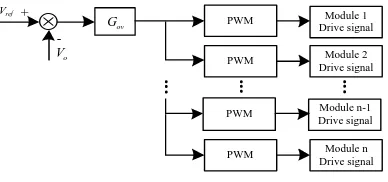
The proposed control strategy is assessed by considering the impact of mismatches among modules, and transient operating conditions in the ISIPOS DC/DC converter. To assess the performance improvement offered when the converter is regulated using the proposed three-loop control scheme, simulation results are compared with those obtained from the widely used common duty-cycle control scheme shown in Fig.8 [14, 15].
-ref
V
o
V
PWM
PWM
PWM
GovModule 1 Drive signal
Module 2 Drive signal
Module n Drive signal
+
PWM Module n-1 Drive signal
Fig. 8. Common duty-cycle control
The test system, shown in Fig.1, consists of an ISIPOS DC/DC converter with rated output power of 1MW. Mismatched parameters, including input capacitance, transformer turns ratio, output inductance and capacitance, as specified in Table 1, are introduced to test the effectiveness of the power balancing function.
TABLE I. SIMULATION AND EXPERIMENTAL SYSTEM PARAMETERS
Parameter Values
Simulation Experiment
DC/DC Converter Rated Power 1MW 100W Input DC Voltage 2200V 40V
Number of Modules 4 4
Input Capacitance Cd1 = Cd2 =
50μF 80μF
Cd1 = Cd2 =
40μF 10μF Transformer Turns Ratio
T1 = T2 = T3 = T4 =
1:6.8 1:6.4 1:6 1:6.4
T1 = T2 = T3 = T4 =
1:1.4 1:1.2 1:1.3 1:1.2 Output Inductance
L1 =
L2 =
L3 =
L4 =
0.05H 0.06H 0.06H 0.05H
L1 = L2 = L3 = L4 =
6.8mH 5.0mH 5.9mH 6.3mH Output Capacitance
C1 = C2 = C3 = C4 =
300μF 350μF 300μF 330μF
C1 = C2 = C3 = C4 =
160μF 160μF 200μF 200μF PWM Carrier Frequency 2.5kHz 2.5kHz
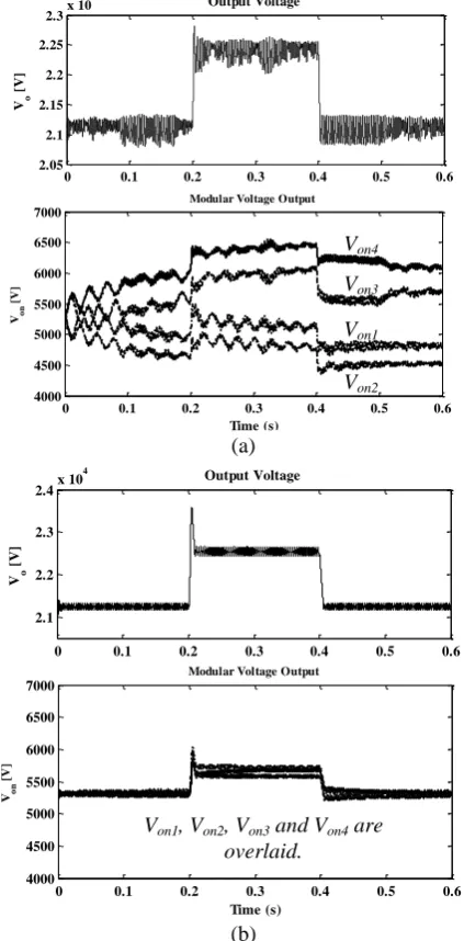
For the simulation validation, the control schemes are tested by applying a step change in load voltage reference from 21.2kV to 22.5kV at t=0.2ms and back to 21.2kV at
t=0.4ms, with system parameter mismatch conditions summarized in Table I. Fig.9 (a) shows the load voltage and individual module output voltages (vo1, vo2, vo3 and vo4) under the common duty-cycle control scheme, and Fig.9 (b) shows the performance of the proposed control scheme. The simulation results show that the performance of the common duty-cycle control strategy is significantly affected by the mismatches. With this control scheme the output voltages of all modules exhibit significant voltage ripple, with a worst-case peak voltage ripple value of approximately 14.7% of the average load voltage. Conversely, the proposed control scheme is able to compensate the mismatch, since the sharing loop enables adjustment of the duty ratio of each individual module so that each module can achieve the same output voltage. Output performances can be further improved by interleaving the modules’ control systems. These results have demonstrated that with the proposed input power balancing control scheme is able to compensate for any negative influences of system parameters mismatch.
A scaled-down experimental rig of ISIPOS with four modules is built to validate the proposed control scheme. Fig.11 shows the two output voltage being regulated at the desired reference value of 60V with common duty-cycle control and proposed control scheme respectively. It indicates that without the dedicated input voltage and current control, each module operates at different voltages
Vo1=16.1V, Vo1=16.9V, Vo1=12.8V and Vo1=14.2V. By virtue
[image:6.595.62.256.514.605.2]0 0.1 0.2 0.3 0.4 0.5 0.6 2.05
2.1 2.15 2.2 2.25
2.3x 10
4
Vo
[
V
]
Output Voltage
0 0.1 0.2 0.3 0.4 0.5 0.6
4000 4500 5000 5500 6000 6500 7000
Time (s)
Von
[V
]
Modular Voltage Output
(a)
0 0.1 0.2 0.3 0.4 0.5 0.6
4000 4500 5000 5500 6000 6500 7000
Time (s)
Von
[V
]
Modular Voltage Output
0 0.1 0.2 0.3 0.4 0.5 0.6
2.1 2.2 2.3 2.4x 10
4
Vo
[
V
]
Output Voltage
[image:7.595.316.565.56.172.2](b)
Fig. 9. Simulated response to a step change in load voltage, with mismatched parameters (a) common duty-cycle control (b) proposed control
Fig. 10.ISIPOS connected full-bridge DC/DC converter test rig
20 ms/div, 5 V/div (a)
[image:7.595.47.259.58.488.2]20 ms/div, 5 V/div (b)
Fig. 11.Experiment resullt (a) with common duty-cycle control and (b) with proposed control
10V
0V
10 ms/div, 2 V/div (a)
12 V 14V
10 ms/div, 5 V/div (b)
Fig. 12.Experiment resullt with proposed control (a) closed loop start-up transient and open loop load step-up transient
V. CONCLUSIONS
A new modular DC/DC converter with ISIPOS connection is proposed with ability to further expand the benefits of parallel-series connection of low power rating modules. Primarily, an active input side control scheme for converter power sharing is addressed. For the load voltage control, the linearized control scheme offered by the Lyapunov control law reduces complexity and ensures improved transient response which is robust to load and input and parameter variations when compared to a linear control technique. The power sharing loops ensure input current sharing among the series connected modules, and input voltage sharing among the parallel connected modules. System-level simulation and scaled-down experimental validation are performed to verify the modeling and control schemes. It is verified that the proposed control, in ISIPOS DC/DC converter, is reliable for stable control and uniform sharing.
REFERENCES
[1] R. Ayyanar, R. Giri, and N. Mohan, "Active input-voltage and load-current sharing in input-series and output-parallel connected modular DC-DC converters using dynamic input-voltage reference scheme," Power Electronics, IEEE Transactions on, vol. 19, pp. 1462-1473, 2004.
[2] P. Monjean, J. Delanoe, D. Marin, J. Auguste, C. Saudemont, and B. Robyns, "Control strategies of DC-based offshore wind farm," in Power Electronics and Applications (EPE 2011),
Von4
Von3
Von1
Von2
[image:7.595.322.560.213.342.2] [image:7.595.51.266.531.672.2]Proceedings of the 2011-14th European Conference on, 2011, pp. 1-9.
[3] L. Yiqing and S. J. Finney, "DC collection networks for offshore generation," in Renewable Power Generation Conference (RPG 2013), 2nd IET, 2013, pp. 1-4.
[4] T. Kjellqvist, S. Norrga, and S. Ostlund, "Design considerations for a medium frequency transformer in a line side power conversion system," in Power Electronics Specialists Conference, 2004. PESC 04. 2004 IEEE 35th Annual, 2004, pp. 704-710 Vol.1. [5] S. P. Engel, M. Stieneker, N. Soltau, S. Rabiee, H.
Stagge, and R. W. De Doncker, "Comparison of the Modular Multilevel DC Converter and the Dual-Active Bridge Converter for Power Conversion in HVDC and MVDC Grids," Power Electronics, IEEE Transactions on, vol. 30, pp. 124-137, 2015.
[6] S. Chunwei, R. Zhao, L. Wangqing, and Z. Zheng, "A novel control strategy for input-parallel-output-series inverter system," in Electrical Machines and Systems (ICEMS), 2011 International Conference on, 2011, pp. 1-5.
[7] R. Xinbo, C. Wu, C. Lulu, C. K. Tse, Y. Hong, and Z. Tao, "Control Strategy for Input-Series&Output-Parallel Converters," Industrial Electronics, IEEE Transactions on, vol. 56, pp. 1174-1185, 2009. [8] C. Wu, R. Xinbo, Y. Hong, and C. K. Tse,
"DC/DC Conversion Systems Consisting of Multiple Converter Modules: Stability, Control, and Experimental Verifications," Power Electronics, IEEE Transactions on, vol. 24, pp. 1463-1474, 2009.
[9] Y. Hong, R. Xinbo, and C. Wu, "The input voltage sharing control strategy for input-series and output-parallel converter under extreme conditions," in Energy Conversion Congress and Exposition, 2009. ECCE 2009. IEEE, 2009, pp. 662-667.
[10] R. Xinbo, C. Lulu, and Z. Tao, "Control Strategy for Input-Series Output-Paralleled Converter," in Power Electronics Specialists Conference, 2006. PESC '06. 37th IEEE, 2006, pp. 1-8.
[11] S. Deshang, D. Kai, and L. Xiaozhong, "Duty Cycle Exchanging Control for Input-Series-Output-Series Connected Two PS-FB DC-DC Converters," Power Electronics, IEEE Transactions on, vol. 27, pp. 1490-1501, 2012.
[12] J. T. Matysik, "A New Method of Integration Control With Instantaneous Current Monitoring for Class D Series-Resonant Converter," Industrial Electronics, IEEE Transactions on, vol. 53, pp. 1564-1576, 2006.
[13] A. A. Aboushady, "Design, analysis and modelling of modular medium-voltage DC/DC converter based systems," Degree of Doctoer of Philosophy, Departement of Electronics and Electrical Engineering, University of Strathclyde, Glasgow, 2012.
[14] S. Jianjiang, L. Jie, and H. Xiangning, "Common-Duty-Ratio Control of Input-Series Output-Parallel Connected Phase-shift Full-Bridge DC–DC Converter Modules," Power Electronics, IEEE Transactions on, vol. 26, pp. 3318-3329, 2011.