Rochester Institute of Technology
RIT Scholar Works
Theses Thesis/Dissertation Collections
2005
0.18?m high performance CMOS process
optimization
Zeki Gurcan
Follow this and additional works at:http://scholarworks.rit.edu/theses
This Thesis is brought to you for free and open access by the Thesis/Dissertation Collections at RIT Scholar Works. It has been accepted for inclusion in Theses by an authorized administrator of RIT Scholar Works. For more information, please [email protected].
Recommended Citation
0.18µm High Performance CMOS Process Optimization for
Manufacturability
By
Zeki B. Gurcan
A Thesis Submitted in Partial Fulfillment of the Requirements for the Degree of
Master of Science in Microelectronic Engineering
Approved by:
Prof. _____________________________ Dr. Lynn Fuller (Thesis Advisor)
Prof. _____________________________ Dr. Karl D. Hirschman (Committee Member)
Prof. _____________________________ Dr. Santosh K. Kurinec (Committee Member)
Paul Fearon, Senior Engineering Manager (External Collaborator)
DEPARTMENT OF MICROELECTRONIC ENGINEERING
COLLEGE OF ENGINEERING
ROCHESTER INSTITUTE OF TECHNOLOGY
ROCHESTER, NEW YORK
0.18µm High Performance CMOS Process Optimization for
Manufacturability
By
Zeki B. Gurcan
I, Zeki B. Gurcan, hereby grant permission to the Wallace Memorial Library of the Rochester Institute of Technology to reproduce this document in whole or in part that any reproduction will not be for commercial use or profit.
___________________ ____________________
Table of Contents
LIST OF FIGURES v
LIST OF TABLES viii
ABSTRACT ix
ACKNOWLEDGEMENTS x
LIST OF DEFINITIONS xi
CHAPTER 1 – INTRODUCTION AND MOTIVATION 1 1.0 Long Channel vs. Short Channel Transistor 2 1.1 Long Channel Threshold Voltage and Saturation Current 4 1.2 Short Channel Effects: Effective Mobility 5
1.3 Channel Length Modulation 6
1.4 Short Channel Effects: Velocity Saturation 7 1.5 Short Channel Effects: VT Roll-off and reduction 8 1.6 Short Channel Effects: Punchthrough & DIBL 11 1.7 Channel Effects: Hot Carrier Injection 11
CHAPTER 2 – TECHNOLOGY OVERVIEW 13
2.0 Process Flow Analysis 14
2.1 Electrical Analysis 24
CHAPTER 3 – SIX SIGMA METHODOLOGY 29
3.0 Define 32
3.1 Measure 35
3.2 Analyze 46
3.3.0 DOE1 51
3.3.1 DOE2 60
3.3.2 DOE3 66
3.3.3 DOE4 70
3.4 Control 72
CHAPTER 4 – SUMMARY OF RESULTS 74
4.0 Conclusion 80
4.1 Future Work 82
REFERENCES 84
APPENDIX A – DOE1 Data 87
APPENDIX B – DOE2 Data 94
APPENDIX C – DOE3 Data 97
APPENDIX D – DOE4 Data 99
LIST OF FIGURES
Figure 1.0.0: MOSFET Channel Length vs. Power Supply, Threshold Voltage (V) and
Gate-Oxide Thickness. 1
Figure 1.0.1: Long Channel vs. Short Channel Extensions. 2 Figure 1.0.2: (a)Long Channel vs. (b) Short Channel Surface Potential Illustration.3 Figure 1.3.0: VDS vs. IDS curve with and without CLM. 7 Figure 1.4.0: Drift Velocity as a function of the lateral electric field. 8
Figure 1.5.0: L vs. VT by increasing VDS. 9
Figure 1.5.1: L vs. VT by increasing VDS [18] 10
Figure 1.6.0: VGS vs. ID with an increased VDS [10] 11
Figure 1.7.0: VGS vs. ID with an increased VDS 12
Figure: 2.0.0: Pad oxide growth and Nitride deposition 14 Figure: 2.0.1: Trench Etch after trench patterning. 15
Figure: 2.0.2: STI Oxide Fill. 15
Figure: 2.0.3: STI after CMP 15
Figure: 2.0.4: Sacrificial oxide growth. 16
Figure: 2.0.5: N-well and NWAPT implants. 16
Figure: 2.0.6:P-well and PWAPT implants. 17
Figure: 2.0.7: Sacrificial oxide removal and first gate oxide growth. 17 Figure: 2.0.8: First gate oxide removal in the low voltage transistor areas. 17 Figure: 2.0.9: First gate oxide is kept in high voltage transistor areas. 18
Figure: 2.0.10: Second gate oxide growth. 18
Figure: 2.0.11: Core NMOS vs. High Voltage NMOS Gate Oxide comparison. 18
Figure: 2.0.12: Poly-silicon deposition 19
Figure: 2.0.13: Poly etch. 19
Figure: 2.0.14: Seal oxide growth 19
Figure: 2.0.15: PMOS PLDD and PHALO implants 20
Figure: 2.0.16: HNLDD and HNHALO implants for high voltage transistors only. 20 Figure: 2.0.17: NLDD and NHALO implants for core NMOS transistors only. 21
Figure: 2.0.18: Spacer deposition. 21
Figure: 2.0.19: Spacer Etch 22
Figure: 2.0.20: N+ implant 22
Figure: 2.0.21: P+ implant 22
Figure: 2.0.22: Final RTP process. 23
Figure: 2.0.23: Final transistor micrograph. 23
Figure: 2.1.0: VDS vs ID with varying VG 24
Figure: 2.1.1: VG vs. ID to meausure VTlin 25
Figure: 2.1.2: VG vs. ID and ISUB due to HCI. 26
Figure: 2.1.3: VD vs. Rout with varying VG 26
Figure: 2.1.4: VDS vs ID with varying VG 27
Figure: 2.1.5: Reverse Short Channel Effect – L vs. VT (VTP= Core PMOS VT, VTN, Core NMOS VT, VTP7= High Voltage PMOS VT, VTN7, High Voltage NMOS VT) 27 Figure: 2.1.6: L. vs. IDSAT for various transistors.(IDSATN= Core NMOS IDSAT, IDSATP=Core PMOS IDSAT, IDSATP7= High Voltage PMOS IDSAT,
Figure: 3.0.0: Technical definition or “Six Sigma” by Motorola Corp. [14] 29
Figure: 3.0.1: Continues improvement cycle. 30
Figure: 3.0.2: Six Sigma DMAIC Process [14]. 31
Figure 3.0.3: Stakeholder Analysis 33
Figure 3.0.4: CTQ Tree 34
Figure 3.0.5: Supplier, Input, Process, Output, Customer Chart (SIPOC). 35
Figure 3.1.0: ET Loss Pareto 36
Figure 3.1.1: ET Scribe-street test structures. 36
Figure 3.1.2: Linear VT test sample graph. 37
Figure 3.1.3: Fully saturated drain current measurement. 38
Figure 3.1.4: Extrapolated leakage measurement. 39
Figure 3.1.5: (a) VTN distribution, (b) VTP distribution 40. Figure 3.1.6: (a) N6_VTX distribution, (b) P7_VTX distribution. 41 Figure 3.1.7: (a) IDSATN distribution, (b) IDSATP distribution. 42 Figure 3.1.8: (a) N6_IDSAT distribution, (b) P7_IDSAT distribution. 43 Figure 3.1.9: (a) Log(IDSSXN) distribution, (b) Log(IDSSXP) distribution. 44 Figure 3.1.10: (a) Log(N6_IDSSX) distribution, (b) Log(P7_IDSSX) distribution. 44 Figure 3.2.0: IDSATP Timeplot with REML Variance analysis 46 Figure 3.2.1: VTN Timeplot with REML Variance analysis 47 Figure 3.2.2: N6_VTX Timeplot with REML Variance analysis 47 Figure 3.2.3: VTP Timeplot with REML Variance analysis 48 Figure 3.2.4: P7_IDSAT Timeplot with REML Variance analysis 48 Figure 3.2.5: IDSATP by wafer from various RTP tools/chambers. 49
Figure 3.2.6: Process Map 50
Figure 3.3.0: High level guideline for setting up an experiment [14]. 51 Figure 3.3.1: Box-Behnken design duplicated for each Poly CD target. 54 Figure 3.3.2: Poly CD factor setup across wafer with selected ET sample locations. 54
Figure 3.3.3:IDSATP Response 55
Figure 3.3.4: VTP Response 56
Figure 3.3.5: VTN Response 56
Figure 3.3.6: RTP Temperature vs. (a) IDSATP St. Dev. (b) IDSSXP St. Dev. 57 Figure 3.3.7: RTP Temperature vs. (a) IDSATP St. Dev. (b) IDSSXP St. Dev. 57
Figure 3.3.8: RTP temperature vs. VTP St. Dev. 58
Figure 3.3.9: DOE1 factors vs. (a) VTP and (b) IDSATP responses 58 Figure 3.3.10: DOE1 factors vs. (a) IDSSXP and (b) IDSSXN responses (c) IDSATN and
(d) VTN responses 59
Figure 3.3.11: PHALO, PLDD, NWAPT vs. (a)IDSATP and (b)VTP 61 Figure 3.3.12: HALO, LDD, APT implant vs. (a) IDSSXP and (b) IDSSXN 61 Figure 3.3.13: NHALO, NLDD, PWAPT vs. (a)IDSATN and (b)VTN 61 Figure 3.3.14: Low and High Voltage NMOS transistors with different implants. 62 Figure 3.3.15: PWAPT energy vs. (a) VTN and (b) IDSATN. 63 Figure 3.3.16: PWAPT energy vs. high voltage (a) N6_VTN and (b)N6_IDSAT 64 Figure 3.3.17: Prediction profiler (a) IDSATN, VTN and (b)N6_IDSAT, N6)VTX as
Figure 3.3.18: Prediction profiler (a) IDSATN, VTN and (b)N6_IDSAT, N6)VTX as
function of APT and HALO implants. 65
Figure 3.3.19: Interaction profiles of RTP time and temperature to (a) VTP, (b) IDSATP 67
Figure 3.3.20: Interaction profiles of RTP time and temperature to (a) VTN, (b) IDSATN 67
Figure 3.3.21: Prediction profiler of RTP Time and Temperature (a) IDSATP, VTP and
(b) IDSATN, VTN. 68
Figure 3.3.22: RTP Time at various temperatures vs. (a) IDSATP mean and (b) St. Dev. 68 Figure 3.3.23: RTP Time at various temperatures vs. (a) VTP and (b) VTN. 69 Figure 3.3.24: RTP Time at various temperatures vs. (a) P+ Composite resistor and (b)
P+ PLY resistor. 69
Figure 3.3.25: Spacer Over-Etch (sec) vs. (a) VTN and (b) IDSATN 70 Figure 3.3.26: Spacer Over-Etch (sec) vs. (a) VTP and (b) IDSATP 71 Figure 3.3.27: Spacer Over-Etch (sec) vs. (a) N6_VTX and (b) N6_IDSAT 71 Figure 3.3.28: Spacer Over-Etch (sec) vs. (a) P7_VTX and (b) P7_IDSAT 71 Figure 3.3.29: Spacer Over-Etch (sec) vs. (a) P+ Composite Resistor and (b) P+ poly
resistor. 72
Figure 3.4.0: (a) Gate oxide thickness, (b) Poly CD control charts. 73 Figure 3.4.1: (a) RTP, (b) Nitride thickness control charts. 73
Figure 3.4.2: Spacer Etch Control Chart 73
Figure 4.0.0: VTN (a) old, (b) new distribution. 75 Figure 4.0.1: IDSATN (a) old, (b) new distribution. 76 Figure 4.0.2: VTP (a) old, (b) new distribution. 76 Figure 4.0.3: IDSATP (a) old, (b) new distribution 77 Figure 4.0.4: N6_VTN (a) old, (b) new distribution 77 Figure 4.0.5: N6_IDSATN (a) old, (b) new distribution. 78 Figure 4.0.6: P7_VTP (a) old, (b) new distribution. 78 Figure 4.0.7: P7_IDSATP (a) old, (b) new distribution. 79 Figure 4.0.8: IDSSXN (a) old, (b) new distribution. 79 Figure 4.0.9: IDSSXP (a) old, (b) new distribution. 80
LIST OF TABLES
Table 3.1.0: ET Parametric Cp and CpK Summary. 45
Table 3.1.2: XY-QFD Table 45
Table 3.3.0: DOE1 Factors 52
Table 3.3.1: DOE1 Setup without the Poly CD variation. 53
Table 3.3.2: DOE2 design for both NMOS and PMOS 60
Table 3.3.3: DOE2 NMOS and PMOS Response Summary 62 Table 3.3.5: DOE3 Design with RTP Temperature and Time as factors. 66
Table 3.3.6: Spacer Over- Etch DOE. 70
Abstract
Complementary metal oxide semiconductor (CMOS) is the most widely used
discrete structure in the semiconductor sector. Low static power consumption, full-rail
high/low voltage transfer characteristics as well as its ease of scaling creates the perfect
combination for the high performance integrated circuits (IC). Today’s challenging
semiconductor industry profile brings the deadlines earlier than expected as a result of the
shorter time-to- market plans as well as limited lifetime on sophisticated ICs. Process
optimization for manufacturability is one of the most challenging issues in the
semiconductor industry since the adoption of the sub- micron CMOS technology.
Process technologies often times gets released with- in tight project schedules
without jeopardizing the quality and customer’s trust. Manufacturing facilities often
times institute very strict process controls in order to achieve the quality and the high
yields. At the same time they take the financial burden of throwing away the
nonconforming material which does not meet the ir specifications. Improving the device
performance becomes the responsibility of the Integration/Device engineering through a
series of process characterization studies.
This paper outlines the various 0.18 µm. CMOS technology issues such as
threshold voltage and saturation current control, and proposes methods to optimize the
process through a series of characterization studies.
6-Sigma-DMAIC process was explored in order to achieve the desired goal.
Techniques described in this thesis could be used in any manufacturing or development
Acknowledgement s
I would like to thank Dr. Lynn Fuller for accepting to be my advisor and
providing support during my studies at R.I.T. I would like to also thank Dr.
Santosh Kurinec and Dr. Karl Hirschman for accepting to be part of my thesis
committee.
I also would like to acknowledge Paul Fearon and Todd Thiheauld for
their technical support. They provided years of experience and expertise as part of
the National Semiconductor’s key technologists. My engineer friends Jerald Rock,
Kendra Crocker and Kenneth Lewis provided unmatchable support in running the
experiments as well as putting in the hard work to improve the unit processes
which are important to the technology.
Special thanks to Dr. Renan Turkman who got me interested in the field of
Device Engineering. I consider his lecture notes as a MOSFET “Bible” and will
always remember him as one of the greatest teachers that I have ever had a chance
List of Definitions
n POR: Process of Record
n POLY FICD: Final Critical Dimension fo r a Poly Line.
n Gate TOX: Gate Oxide Thickness
n NWAPT: N+ Well Anti-Punch through Implant
n PWAPT: P+ Well Anti-Punch through Implant
n NLDD: N+ Lightly Doped Drain.
n PLDD: P+ Lightly Doped Drain.
n NHALO: N+ HALO Implant
n PHALO: P+ HALO Implant
n HNHALO: High Voltage Transistor N+ HALO Implant
n DIBL: Drain Induced Barrier Lowering.
n DGO: Double Gate Oxide, high voltage transistor module.
n HCI: Hot Carrier Injection.
n PCA: Poly to Poly Capacitor.
n Critical to Quality (CTQ): Is a key measurable characteristic of a product,
process or service whose performance standards must be met in order to
Chapter 1
Introduction and Motivation
CMOSTransistor dimensions are getting smaller and smaller as Moore’s Law of
doubling the number of transistors every four years is still in affect. As MOSFET channel
length (L) scales down to sub- micron dimensions as described in Figure 1.0, the Power
supply (Vdd) and Threshold Voltage (VT) values get smaller and the Gate-oxide thickness becomes thinner. This phenomenon is referred to as “Scaling” with a scaling factor
calculation of:
Figure 1.0.0: MOSFET Channel Length vs. Power Supply, Threshold Voltage (V) and
Gate-Oxide Thickness1
1
“Scaling” in semiconductors come with a big price tag, not only during the
development phase but also during the manufacturing lifetime of the technology. Most
advanced semiconductor manufacturing is currently (2005) is pushing the channel length
dimensions of 65 nm. however the content of this thesis is going to focus on optimizing
the performance of a main stream 0.18µm CMOS technology node. Based on the Figure
1.0.0, this would place the discussion around a 3-5 nm gate-oxide thickness, 0.4-0.5 V
Threshold Voltage and a supply voltage of 1.8 – 2.0 V.
1.0 Long Channel vs. Short Channel Transistor
0.18µm CMOS technology is a node where the difference between the long
channel transistor and the short channel counterpart becomes significant. Long channel
transistor assumes a uniformly doped channel profiles with no gate leakage as well as a
source-to-bulk or drain-to-bulk leakage currents. Channel width (W) is wide enough to
ignore any dopant and electric field crowding at the edge of the isolation which would
impact the electrical test parameters. The length of the channel is such that it is much
greater than the source-to-bulk transition regions which may be as much as 0.2 µm. The
effect of the horizontal electric field (
ε
x) could be ignored in the case of long channel transistors since is much smaller than the vertical electric field (ε
y).Figure 1.0.1: Long Channel vs. Short Channel Extensions.
Short channel transistor study however can not ignore
ε
x since it is not muchε
P-well
S - N+ S- N+
P-well
y
ε
ε
x
Long channel Short channel
P-well
S - N+ S- N+
P-well
y
ε
ε
x
P-well
S - N+ S- N+
P-well
y
ε
ε
x
drain regions. Channel regions are not assumed to be uniformly doped as the influence of
the source and drain regions are starting to increase. Short channel effects such as drain
induced barrier lowering (DIBL), velocity saturation, threshold voltage reduction, VT
roll-off, hot carrier injection and punch-through current starts to take place.
In theory, the goal of all Device Engineers is to make a short channel transistor
with a small channel length behave like a long channel transistor by engineering the
channel regions of the transistors in order to control the substrate surface potential (?s).
?s near the source region is typically at Fbi which is in the order of 66mV. as ?s near
the drain region is typically about VDS higher than the Fbi. Assuming no gate bias, the
surface potential in the long channel transistor should be the same everywhere as
illustrated on Figure 1.0.2 (a).
Figure 1.0.2: (a) Long Channel vs. (b) Short Channel Surface Potential
Illustration.
x
N+ source N+ drain
x
N+ source N+ drain
X=0
X=0 ?s(x)
?s(x) Long Channel
Short Channel
?slc
?slc
Fbi Fbi
VDS+ Fbi
VDS+ Fbi
(a)
(b)
X=L
X=L x
N+ source N+ drain
x
N+ source N+ drain
X=0
X=0 ?s(x)
?s(x) Long Channel
Short Channel
?slc
?slc
Fbi Fbi
VDS+ Fbi
VDS+ Fbi
(a)
(b)
X=L
?s for the short channel transistor exhibits a much different behavior than the
long channel transistor due to the proximity effect of the drain regions and the thin gate
oxides. Overall ?sis higher for short channel devices which make it easier to turn on the
transistors.
1.1 Long Channel Threshold Voltage and Saturation Current
Due to the assumptions mentioned in Section 1.0, the long channel transistorsaturation current ignores many of the short channel effects. Drain current (IDS)
expression is derived by assuming that the overall current flow is as a result of the drift
current density when the source end of the transistor is fully inverted. IDS vary linearly as
the channel surface goes into moderate to weak inversion yielding equation (1). Once the
drain voltage (VDS) goes above a value in which the drain region is no longer strongly inverted but more weakly inverted or depleted. ?s becomes insensitive to VDS which pushes the transistor into the saturation mode of operation expressed in equation (2) [8]:
Note IDS is a function of the channel length (L), channel width (W), gate oxide
capacitance per unit area (C’ox) and the electron mobility (µ). IDS also depend on the
long channel threshold voltage (VT) at which the amount of current flow through the
channel is significant.
Mobility W
L µC’ox (VGS-VT)VDS- VDS 2
2
W
L µC’ox
(VGS-VT)2 2
I
DS Linear=
I
DS Saturation=
(1)
(2) Oxide capacitance per unit area
Long Channel Threshold Voltage Mobility
W
L µC’ox (VGS-VT)VDS- VDS 2
2
W
L µC’ox
(VGS-VT)2 2
I
DS Linear=
I
DS Saturation=
(1)
(2) Oxide capacitance per unit area
Long Channel Threshold Voltage W
L µC’ox (VGS-VT)VDS- VDS 2
2
W
L µC’ox
(VGS-VT)2 2
I
DS Linear=
I
DS Saturation=
(1)
(2) Oxide capacitance per unit area
Equation (3) outlines the long channel threshold voltage (VTLC) where VFB is the flat band voltage which is typically around -1V (Fms = metal-to-semiconductor work
function), FF is the Fermi potential which is around 0.56V and Ft of 26mV at 300 °K [2].
1.2 Short Channel Effects: Effective Mobility
Mobility of the electrons in the channel region is lower than the bulk silicon due
to high electron-electron scattering at the interface, poor silicon quality at the surface
(defects due to ion implants) as well as the high
ε
y causing surface scattering in thechanne l. This phenomenon limits the amount of current flow in the channel during
transistor operation. Effective mobility could be calculated as described in formula (6):
One can influence the effective mobility by changing the gate oxide thickness,
thresho ld adjust implant as well as the screen oxide thickness which effectively plays in
an important role in the quality of the silicon in the channel region.
)
(
2
4
'
TLC FB B SB B
B F t
A
V
V
V
F N
Cox
φ
γ
φ
φ
φ
φ
γ
==
+ +
+
+
@
(3) (4) (5) )(
2
4
'
TLC FB B SB B
B F t
A
V
V
V
F N
Cox
φ
γ
φ
φ
φ
φ
γ
==
+ +
+
+
@
(3) (4) (5)µ
eff=
µ
o(1+?(V
GS-V
T)
Effective Mobility
1.3 Channel Length Modulation
Channel length modulation (CLM) is the increase in the drain current in the
saturation region due to the reduction in the gradual channel length b y ? L. Channel is in
pinchoff mode at which the channel surface is fully inverted when the drain voltage
reaches VDSSAT. As the voltage at the drain side continues to increase, the channel region at the drain side goes into depletion. Electrons which leave the inversion layer get swept
across this depletion region causing the drain current to increase. The width of the
depletion region in the drain end is the driving force behind the effective channel length
reduction by ? L.
CLM parameter of lambda (?) is calculated by using the early voltage (VA) and VDSSAT as shown on Figure 1.3.0. VDSSAT could be ignored in most cases since VA is much larger in magnitude. ? is used to help quantify the increase in the saturation current
as described in equation (9).
a
?~
µ
ov
th~
~
~ 0.0125um/V
Low field mobility
Thermal Electron Velocity (7)
?=
a
?C
OX’
Figure 1.3.0: VDS vs. IDS curve with and without CLM
1.4 Short Channel Effects: Velocity Saturation
As channel length is reduced, the lateral fields inside the channel become large.
Once the lateral electric field towards the drain side exceeds a critical field value,
electrons start to collide with the silicon atoms and loose their energy. Drift velocity
starts to saturate and is no longer proportional to the lateral fields which described in
Figure 1.4.0. Velocity saturation causes further mobility degradation in channel region
towards the drain area. [9]
Modified IDS current expression due to velocity saturation phenomenon can be seen on formulas (10) and (11). In short channel devices, the term VDS/L is several times larger than ESAT [8] which significantly reduces the linear IDS.
V
DSI
DSV
DSsatV
DSV
AI
D’I
D? = 1/(VA-VDSsat)
With CLM
Without CLM
V
DSI
DSV
DSsatV
DSV
AI
D’I
D? = 1/(VA-VDSsat)
With CLM
Without CLM
W
L µC’ox
(VGS-VT)2 2
I
DS Saturation=
[1+?(VDS-VDSsat)] (9)CLM Factor
W
L µC’ox
(VGS-VT)2 2
I
DS Saturation=
W [1+?(VDS-VDSsat)] (9)L µC’ox
(VGS-VT)2 2
I
DS Saturation=
[1+?(VDS-VDSsat)] (9)Figure 1.4.0: Drift Velocity as a function of the lateral electric field.
As L approaches zero, the IDS saturation expression on (11) looses its square law behavior which causes IDS to increase linearly with increased gate voltage.
1.5 Short Channel Effects: VT Roll-off and reduction
Due to the proximity of the drain and source regions in short channel devices as
illustrated on Figure 1.0.2.b, the gate starts to loose control over the channel and the
surface potential (?s) gets higher at any point in the channel region. Increasing ?s in the
channel region is equivalent to decreasing the potential barrier for electrons to overcome
to reach the drain side which inevitably reduces the threshold voltage. This behavior
W L
µeffC’ox (VGS-VT) 2
I
DS Saturation=
(VGS-VT)+L 2
sat
ε
sat
ε
[1+?(VDS-VDSsat)] (11)2
sat
c
ε
=
ε
d maxo
c
ν
µ
ε
=
,
(12)x
ε
cε
V
drift(V/cm)
(cm/sec)
cε
xε
=
@
Slope = µ
omax d
ν
max2
d dν
ν
= xε
cε
V
drift(V/cm)
(cm/sec)
cε
xε
=
@
Slope = µ
omax d
ν
max2
d dν
ν
= WL (VGS-VT)VDS- VDS 2
2
I
DS Linear=
µeffC’ox1+ VDS
L
ε
sat(10) W
L (VGS-VT)VDS- VDS 2
2
I
DS Linear=
µeffC’ox1+ VDS
L
ε
satknown as VT roll-off is described in Figure 1.5.0. As VDS increases, the ?L gets larger and the potential barrier gets lowered. This phenomenon is known as the Drain Induced
Barrier Lowering (DIBL) which makes the transistor turn on easier. Equation (14)
describes the reduction in threshold voltage [17]. Gate oxide thickness, source/drain
junction depth and channel doping concentrations play an important role in VT roll-off.
Channel engineering by adding a lightly doped drain (LDD) implant improves the VT
reduction due to lower drain to substrate junction built in potential as well as the reducing
the effective drain voltage.
Figure 1.5.0: L vs. VT by increasing VDS
SC LC
T
T
T
V
=
V
− ∆
V
(13)(
)
2
2
2
2
T DS bi F
L
L
V
= V
φ
φ
e
e
−
−
∆
+
−
×
+
l
l
(14)L
V
TV
dsV
ds=50mV
L
V
TV
dsV
ds=50mV
V
TAnother important short channel effect which influences the VT is the Reverse
Short Channel Effect (RSCE). This effect has been attributed to the channel doping
profile irregularities and boron pile-up at the source and drain junctions due to the
transient enhanced diffusion [19]. As Leff gets smaller, the increased boron concentration
makes the transistor harder to turn on. Halo implants (also called as pocket implant)
reduces this effect by influencing the doping concentration at the source and drain
transition regions.
Figure 1.5.1: L vs. VT by increasing VDS [18]
ox si
ox
d
t
ε
η
ε
Χ × ×
=
l
(15)2
si(2
F SB)
A
V
d
qN
ε
φ
+
Χ =
(16)L
Reverse ShortChannel Effect
B A
A: Halo Implant
B: Without Halo Implant
L
minL
min’V
TL
Reverse ShortChannel Effect
B A
A: Halo Implant
B: Without Halo Implant
L
minL
min’Lack of halo implant triggers the Figure 1.5.1 L vs. VT behavior. Although gate oxide thickness plays an important role in RSCE, channel engineering is the real answer
in optimizing the transistor.
1.6 Short Channel Effects: Punchthrough & DIBL
The source and drain space charge regions could be problematic in short channel
transistors as Leff gets smaller. Even though the surface doping concentration is
engineered to control device parametrics, the sub-surface behavior of these junctions
could cause significant current flows. This phenomenon is known as “Punchthrough”
which IDS increased with no gate bias with an increased VDS as shown on Figure 1.6.0. High energy anti-punchthrough implant is necessary to influence the channel profile deep
in the silicon. DIBL plays a stronger role, if there is any low gate bias present.
Figure 1.6.0: VGS vs. ID with an increased VDS [10]
1.7 Short Channel Effects: Hot Carrier Injection
Longitudinal electric field increases with the increased drain voltage and
decreased gate oxide thickness. During the saturation mode of operation, electrons
V
gslog Id
V
ds
Punchthrough & DIBL
V
gslog Id
V
ds
leaving the inversion layer at Leff, enters the drain depletion region. As Leff gets smaller and the drain voltage increases, the longitudinal electric field on the drain side gets
higher. As this electric field exceeds the
ε
c described in Figure 1.7.0, the electronscontinue to gain kinetic energy. Some of the electrons loose their energy due to scattering
but some gain enough energy to cause impact ionization upon collision in the drain
region. Electrons with the high energy in the depletion region are called “Hot” carriers
thus called “Hot Carrier Injection”. Electron-hole pair generation as a result of the impact
ionization causes the substrate current (ISUB) and excess interface states in the gate oxide [7].
Figure 1.7.0: VGS vs. ID with an increased VDS
Hot carrier injection could cause long term reliability issues such as long term VT reduction, saturation and leakage current increase. If ISUB is strong enough to increase the voltage drop between the VD and VSUB , it could lead to “snap-back” in the transistor and cause latch-up issues in the product.
Common approach in reducing this phenomenon is to reduce the maximum
electric field in the drain side. This is typically done by double diffused drains or with
LDD implants.
V
SV
GV
DV
SUBn+
n+
P-type Si
Isub
p+
0 V
0.7 V
Id
V
SV
GV
DV
SUBn+
n+
P-type Si
Isub
Isub
p+
0 V
0.7 V
0 V
0.7 V
Id
Chapter 2
Technology Overview
This chapter provides a high level process and electrical analysis overview of the
technology. Process technology studied during this project is an aluminum back-end
0.18µm Twin-Well CMOS process as mentioned during introduction.
Key process specifications as follows:
Twin-Well, N+/P+ Si-Gate Salicided CMOS
5 Metal Layers (Aluminum)
Leff: 0.18µm
Isolation: Shallow Trench Isolation.
Spacer: Nitride spacer.
Optional: Dual Gate Oxide (DGO)
Dual Gate-oxide thickness’ are:
• Low Voltage Transistor: 36A (VDD=1.8V)
• High Voltage Transistor: 75A (VDD= 3.3V)
Process technology utilizes Lightly Doped Drain (LDD) implant, HALO (pocket
implant) and anti-punch thru (APT) implants as well as a graded junction implants to
suppress the short channel effects described in Chapter 1.
LDD Implant; is the most commonly used implant process to reduce Hot Carrier
performance as discussed in Section 1.7. Although this implant goes into both source and
drain regions, the lateral electric field on the drain side gets reduced due to this implant as
a result of the device operation. The type of doping used for PMOS is P-type (BF2) and
for NMOS is N-type (As) at fairly low implant energies (10-15 KeV)
HALO Implant; is the technique used to reduce punchthrough (Substrate DIBL)
in short channel MOSFETS. This implant is locally introduced at the tip of the LDD
regions to better control the substrate doping concentration. As a result, the substrate
doping concentration can be locally increased thus reducing the depletion region between
the N+ to substrate and P+ to substrate.
APT Implant; is also used to reduce punchthrough in short channel MOSFETS. It
can also play the role of the VT adjust implant where it gets implanted right under the
gate oxide thus changing the substrate doping concentration.
2.0 Process Flow Analysis
0.18µm Twin-Well CMOS process is built on a P-type 30 ohm-cm epitaxially
grown starting silicon. Pad oxide and nitride is deposited (Figure: 2.0.0) in order to define
the shallow trench isolation (STI) and transistor width (W).
Figure: 2.0.0: Pad oxide growth and Nitride deposition
Nitride Pad Oxide
Figure: 2.0.1: Trench Etch after trench patterning.
Trench etch into the silicon is followed after the trench patterning as shown on
Figure: 2.0.1. Two step STI oxide fill with various densities is used to cover the trenches
to reduce sidewall stress and dishing before the planarization step (Figure: 2.0.2).
Figure: 2.0.2: STI Oxide Fill.
Chemical mechanical planarization (CMP) is used to polish the excess oxide and
the nitride layer is used to stop the STI CMP process (Figure: 2.0.3). Nitride and the pad
oxide are then stripped off in a wet chemistry.
Figure: 2.0.3: STI after CMP
Trench Etch
STI OXIDE FILL
Sacrificial oxide is grown (Figure: 2.0.4) to protect the silicon surface from
implant damage as well as to prevent implant channeling.
Figure: 2.0.4: Sacrificial oxide growth.
500 KeV, 2.1E13 /cm3 phosphorus implant is performed to create the N-well for PMOS which is followed by a 110 KeV, 3E12 /cm3 phosphorus implant to act as an anti-punchthrough implant (Figure: 2.0.5). Please note that there is no so-called VT adjust implant at this step which is contrary to the traditional PMOS designs. The peak of the
NWAPT implant influences the sub-surface dopant concentration to prevent source-drain
punchthrough; however the tail of this implant controls the surface dopant concentration
which is influencing the transistor VT.
Figure: 2.0.5: N-well and NWAPT implants.
Similar approach is used during the design of the NMOS transistor where no
dedicated VT adjust implant is used. 210 KeV, 2E13/cm3 boron P-well implant is followed by an 80 KeV, 5E12/cm3 boron PWAPT implant before removing the sacrificial oxide (Figure: 2.0.6).
Sacrificial Oxide
photoresist
NWAPT P, 110KeV 3.0E+12 N-well
Figure: 2.0.6:P-well and PWAPT implants.
Two separate gate oxide growth processes is necessary in order to create a high
voltage as well as a low voltage transistor technology. First gate oxide is grown after the
sacrificial oxide removal (Figure: 2.0.7). The first oxide gets removed in the areas where
only low voltage transistors will be present and kept in areas where the high voltage
transistors will exist (Figures: 2.0.7-8-9).
Figure: 2.0.7: Sacrificial oxide removal and first gate oxide growth.
Figure: 2.0.8: First gate oxide removal in the low voltage transistor areas.
photoresist
PWAPT B, 80KeV 5.0E+12
NWAPT P, 110KeV 3.0E+12 N-well
P, 500KeV 2.1E+13 P-well
B, 210KeV 2.0E+13
PWAPT NWAPT
P-well N-well
Sacrificial Oxide Removal First Gate Oxide
PWAPT NWAPT
P-well N-well
Figure: 2.0.9: First gate oxide is kept in high voltage transistor areas.
Second gate oxide thickness of 36A is grown across the wafer to be used as the
gate oxide for the low voltage transistor as shown on Figure 2.0.10.
Figure: 2.0.10: Second gate oxide growth
The second gate oxide in conjunction with the first gate oxide creates the 75A
high voltage transistor gate oxide (Figure: 2.0.11). Dual gate oxide process could be used
to evaluate various oxide thicknesses during the development process.
Figure: 2.0.11: Core NMOS vs. High Voltage NMOS Gate Oxide comparison.
PWAPT P-well
NMOS High Voltage NMOS
PWAPT P-well
photoresist
First Gate Oxide Removal
PWAPT NWAPT
P-well N-well
Gate Oxide ~ 36A
NMOS PMOS
PWAPT P-well
NMOS High Voltage NMOS
PWAPT P-well
Figure: 2.0.12: Poly-silicon deposition
Poly-silicon gate layer is deposited and etched in order to achieve a 0.19µm
drawn channel length and a 0.18 µm Leff for the technology (Figure: 2.0.12-13)
Figure: 2.0.13: Poly etch.
Thin layer of seal oxide is grown to act as a poly-silicon grain structure seal and
for the LDD implant block to prevent channeling (Figure: 2.0.14).
Figure: 2.0.14: Seal oxide growth
Upon seal oxide growth, PLDD implant of BF2 is performed at 10KeV, 8E13/cm3 followed by an arsenic (As) PHALO implant at 150KeV, 2.7E13/cm3 (Figure: 2.0.15).
PWAPT NWAPT
P-well N-well
Poly Deposition
NMOS PMOS
PWAPT NWAPT
P-well N-well
Poly Etch ~ 0.19um
PWAPT NWAPT
P-well N-well
Figure: 2.0.15: PMOS PLDD and PHALO implants
Both core PMOS transistors and the high voltage PMOS transistors receive the
same PLDD and PHALO implants. There are no additional or extra implants for the high
PMOS transistors.
Figure: 2.0.16: HNLDD and HNHALO implants for high voltage trans istors only.
Unlike the PMOS transistor architecture, high voltage NMOS transistors utilize a
separate LDD and HALO implants as described in Figure: 2.0.16. 20KeV, 8.4E13/cm3 P implant is used for HNLDD and 75KeV, 4.4E13/cm3 BF2 implants is used for HNHALO.
photoresist
PWAPT NWAPT
P-well N-well
PLDD BF2, 10KeV 8.0E+13
PHALO As, 150KeV 2.7E+13
NMOS PMOS
photoresist
PWAPT
P-well P-well
HNHALO BF2, 75KeV 4.4E+13 PWAPT
NMOS High Voltage NMOS
Figure: 2.0.17: NLDD and NHALO implants for core NMOS transistors only.
Arsenic is used as the NLDD implant with a 10KeV energy and 5.0E14/cm3 dose followed by a BF2 implant of 75KeV and 1.8E13 /cm3 dose as shown on Figure: 2.0.17.
Thin layer of spacer oxide is deposited under the 1000A of the spacer nitride
deposition. Oxide layer is used to release stress caused by the nitride film and also to act
as an etch stop during spacer etch process (Figure: 2.0.18).
Figure: 2.0.18: Spacer deposition.
Spacer nitride and oxide layers are etched using a reactive ion etch processes to
form the profiles outlined on Figure: 2.0.19.
PWAPT NWAPT
P-well N-well
NLDD PLDD
NHALO PHALO
Spacer Nitride ~ 1000 A
Spacer Oxide
NMOS PMOS
photoresist
PWAPT
P-well P-well
NLDD As, 10KeV 5.0E+14
NHALO BF2, 75KeV
1.8E+13 PWAPT HNHALO
NMOS High Voltage NMOS
Figure: 2.0.19: Spacer Etch
Spacer etch is followed by the N+ and P+ implants respectively. N+ implant is a
50KeV arsenic implant with a 7E15/cm3 dose. P+ implant is 15KeV BF2 implant with a 5E15 /cm3 dose (Figure: 2.0.20-21).
Figure: 2.0.20: N+ implant
Figure: 2.0.21: P+ implant
P-well N-well
STI
NLDD PLDD
PWAPT NWAPT
NMOS PMOS
Spacer Etch
photoresist
NMOS PMOS
P-well N-well
STI N+
NLDD PLDD
PWAPT NWAPT
N+, As 50KeV
7.0E+15 P+
NHALO PHALO
photoresist
NMOS PMOS
P-well N-well
STI
P+ N+
NLDD PLDD
PWAPT NWAPT
N+ P+. BF2, 15KeV 5.0E15
P+ implant process is followed by a thin cap-oxidation process in order to
capsulate the surface of the wafer to prevent out-diffusion of dopants during the final
anneal process. Anneal process is performed at 1075 degC for 12 seconds (Figure:
2.0.22). This part of the process is especially important since only one major thermal step
is used in order to activate the dopants in the technology.
Figure: 2.0.22: Final RTP process.
Figure: 2.0.23 outlines a final transistor cross sectional view a test structure with
the nitride spacer sidewalls.
Figure: 2.0.23: Final transistor micrograph. (TEST STRUCTURE)
N+ P-well
N+ P+
P+
STI
P-well N-well N-well RTP, 1075 degC , 12 sec.
N+ P+
N+ P+
NMOS High Voltage NMOS PMOS High Voltage PMOS
2.1 Electrical Analysis
In order to effectively optimize the manufacturing process, one must study not
only the overall process flow but the electrical characterization as well. This section will
focus on the electrical characterization of the technology under review. Figure 2.1.0
displays the VDS vs. ID with varying VG which is also referred to as “the family of curves”. Family of curves highlight an increase in ID due to ISUB as discussed in Section 1.7. It is important to note that the ID increase due to ISUB doesn’t seem to be a problem up untill VDS values of 2.5V or so on a 1.8V technology. It is important to note the HCI immunity and not disturb the LDD implants during process optimization.
Figure: 2.1.0: VDS vs. ID with varying VG
Figure: 2.1.1 outlines the extrapolated linear threshold voltage (VTlin) calculation from the VG vs. ID measurement. Half of the drain voltage of 50mV is subtracted from the x-axis intercept of the tangent line which is drawn at the maximum slope
(tranconductance). Please note the degradation of the drain current at high gate bias as
mentioned in Section 1.4.
-1.00E-03 0.00E+00 1.00E-03 2.00E-03 3.00E-03 4.00E-03 5.00E-03 6.00E-03
0 1 2 3 4
VDS (V)
ID (A)
VG=1.44V VG=1.08V VG=0.74V VG=0.36V VG=0V
Figure: 2.1.1: VG vs. ID to measure VTlin
Figure: 2.1.2 shows the ISUB dependency to the gate bias. As gate voltage increases, the magnitude of the ISUB increases due to increased longitudinal electric field near the drain side. However, as gate voltage continues to increase, the potential drop
between the gate and the drain notes starts to approach zero causing ISUB to drop. ISUB appears to be worse at gate voltages around 1.4V.
y = 1375.1x - 668.79
0 200 400 600 800 1000 1200 1400 1600
0 0.5 1 1.5 2
VG(V)
ID(uA)
V
Tlin=V
T0-0.050V= 0.485V-0.050V=
0.435V
V
T0=668/1375= 0.485 V
Mobility degradation due to
normal field
Figure: 2.1.2: VG vs. ID and ISUB due to HCI.
It is often times helpful to review the VD vs. Rout by varying VG in an attempt to observe most short channel effects in one chart to compare various transistors with each
other. Figure: 2.1.3 outlines the CLM, DIBL and ISUB noted on this technology.
Figure: 2.1.3: VD vs. Rout with varying VG
0.00E+00 1.00E-03 2.00E-03 3.00E-03 4.00E-03 5.00E-03 6.00E-03 7.00E-03 8.00E-03 9.00E-03 1.00E-02
0 0.5 1 1.5 2 2.5 3
VG (V)
ID (A)
-1.60E-05 -1.40E-05 -1.20E-05 -1.00E-05 -8.00E-06 -6.00E-06 -4.00E-06 -2.00E-06 0.00E+00 2.00E-06
ISUB
ID ISUB
VD=2.5V
0.00E+00 1.00E+03 2.00E+03 3.00E+03 4.00E+03 5.00E+03 6.00E+03
0 1 2 3 4
VD (V)
Rout (ohms)
VG=0.72V VG=1.08V VG=1.44V VG=1.8V
DIBL
ISUB
CLM
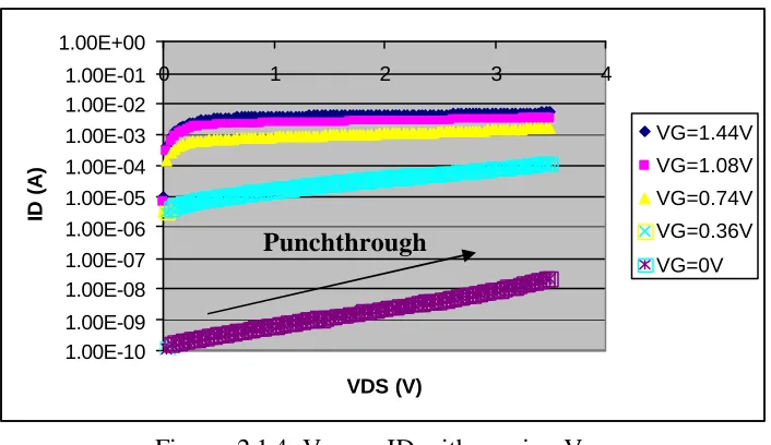
Figure: 2.1.4 shows the drain current observed due to punchthrough effect with
increased VD and VG=0V. Although punchthrough current is low, modifying the APT
implant is going to be somewhat challenging due to the lack of VT adjust implant.
Figure: 2.1.4: VDS vs. ID with varying VG.
Reverse short channel effect can be seen on Figure: 2.1.5 between NMOS and
PMOS transistors as well as the high voltage and core transistors. Halo implants will play
an integral role in controlling this effect as discussed in section 1.5.
Figure: 2.1.5: Reverse Short Channel Effect – L vs. VT (VTP= Core PMOS VT, VTN, Core NMOS VT, VTP7= High Voltage PMOS VT, VTN7, High Voltage NMOS VT)
1.00E-10 1.00E-09 1.00E-08 1.00E-07 1.00E-06 1.00E-05 1.00E-04 1.00E-03 1.00E-02 1.00E-01 1.00E+00
0 1 2 3 4
VDS (V)
ID (A)
VG=1.44V
VG=1.08V
VG=0.74V
VG=0.36V
VG=0V
-0.8 -0.6 -0.4 -0.2 0 0.2 0.4 0.6
0.1 0.5 0.9 1.3 1.7
L (um)
VT (V)
VTP
VTP7 VTN
VTN7
Figure: 2.1.6 outlines the fully saturated drain current (IDSAT) sensitivity to
channel length. As expected both NMOS and PMOS low voltage transistors as more
sensitive to changes in the channel length due to thinner gate oxides and smaller channel
length dimensions.
Figure: 2.1.6: L. vs. IDSAT for various transistors.(IDSATN= Core NMOS IDSAT, IDSATP=Core PMOS IDSAT, IDSATP7= High Voltage PMOS IDSAT,
IDSATP6=High Voltage NMOS IDSAT)
y = -2139x + 987.79 y = -651.67x + 831.13
y = -1520x + 566.12 y = -634.5x + 516.3 200
300 400 500 600 700
0.1 0.2 L (um) 0.3 0.4
ID (uA/um)
IDSATP7
IDSATN6
Chapter 3
Six Sigma Methodology
Both process and electrical analysis is performed to provide the necessary
background to the reader on the core technology challenges and potential precautions.
“Six Sigma” as a problem solving methodology is applied in order to outline the work
accomplished in order to optimize the process.
Technical definition of six sigma is to design a process such that the defective parts
per million opportunity does not exceed 3.4 and a CpK of 2.0 when the process is
centered (Figure: 3.0.0). Process CpK can drift between 1.5 and 2.0 based on the natural
variation of the mean within short periods of time.
Over time, Six Sigma evolved into a breakthrough management tool, whic h
enables companies to increase profits dramatically by streamlining operations, improving
quality, and eliminating defects and mistakes. Six Sigma reduces the variables involved
in a process in order to improve and achieve the goal. The methodology is based on five
steps of DEFINE, MEASURE, ANALYZE, IMPROVE, CONTROL or also referred to
as DMAIC [14].
Figure: 3.0.0: Technical definition or “Six Sigma” by Motorola Corp. [14]
-6σ −5σ −4σ -3σ −2σ −1σ 0 +1σ +2σ +3σ +4σ +5σ +6σ
6
σ
to LSL6
σ
to USLCp=2 Cpk=1.5 Cp=2 Cpk=1.5
Cp=Cpk = 2 ±1.5σ
LSL
12.5% 12.5%
75%
3.4 DPMO 3.4 DPMO
USL
Six sigma provides a highly disciplined process to engineers with the necessary
resources and tools to reach the end goal.. Since the overall objective is to reduce
performance variation and reduce defects in areas that are important to customer, it would
be fair to recommend the overall reduction process outlined in Figure: 3.0.1. It would be
necessary to study the initial Cp and CpK performance to determine the next step for the
process. For instance, process distribution with poor Cp and CpK would require an
improvement in Cp first then an improvement in CpK.
Figure: 3.0.1: Continues improvement cycle.
In an attempt to improve the manufacturing process to the desirable Cp and CpK
values, the DMAIC process outlines in Figure: 3.0.2 will be necessary. Define step
identifies a project suitable for Six Sigma efforts based on business objectives as well as
customer needs. Project stakeholders are defined as well as the critical to quality (CTQ)
parameters based on customer needs. High level supplier, input, process, output,
customer flow is generated to outline the improve ment process for the project. DOE1 to
Reduce Variation –
Improve Cp
DOE2 to Target Process –
Improve CpK
DOE3 to Reduce Variation –
Further Improve Cp
USL
LSL
USL
LSL
USL
LSL USL
LSL UCL
LCL
Bad Cp
Bad Cpk Good CpBad Cpk
Good Cp Good Cpk Best Cp
Best Cpk
Set control
Figure: 3.0.2: Six Sigma DMAIC Process [14].
“Measure” step focuses on the measure of the overall process baseline to help set
goals, measurement techniques. It also provides an opportunity for participants to
perform measurement validation and the study of the measurement systems analysis.
Relationship between the Y-output parameters and the X-inputs parameters gets
determined.
“Analyze ” step drills down to the specifics of the root cause of the variation by
studying the “Measure” step data and mapping out the overall process in question. It is
often possible that during the “Analyze” step, the performance delimiters are eliminated
by placing containment steps. “Improve ” step involves the formal experimentation as a
result of “Measure” and “Analyze” outcomes. It confirms the key variables and
quantifies their effects on the process. “Control” step puts in place the control charts
Definethe Problem, Project Objective, Project Goals, and
Metrics (Ys)linked
to CTQs
PROCESS
PROCESS
X1 X2 X3 X4
Y1
Y2
Y3
Establish Controlson the critical (Xs) so
the improvements will be maintained
Identify ways to Improve
the process and validate the solution
Measure and Analyze
data and process performance to determine
the critical variables and
root cause of the
based on the maximum acceptable process limits. It is highly desirable to understand the
process variations and interactions during “Improve” step I order to deliver the most
robust technology.
3.0 Define
DEFINE step is one of the most important steps in the process. At this step the
project goals are established and both the internal and external customers are determined.
High level deliverables that are associated with this step are:
1. Problem statement, objective, goals and benefits.
2. Critical to quality (CTQ) parameters.
3. Stakeholder Analysis.
4. Supplier, Input, Process, Output, Customer (SIPOC) relationship.
Problem statement for this project could be states as “Core 0.18um process
technology is experiencing excessive cumulative yield loss which is impacting the overall
site financials.”
Objective of the project is to determine the root caus e of the yield loss using the
DMAIC process to identify the process control parameters to reduce variation.
Benefits of this project are to increased yield and ultimately the revenue for the
site. Internal customer satisfaction will also be a side benefit for this project.
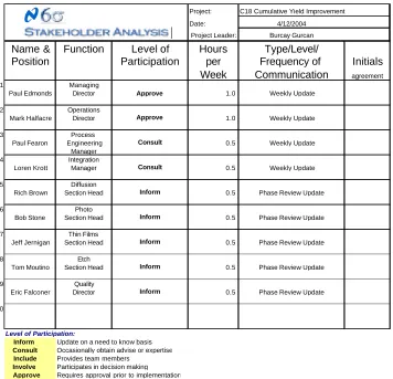
Stakeholder analysis (Figure 3.0.3) is performed in order to determine the
individual who have a stake in the outcome of the project. They will have direct influence
Project: C18 Cumulative Yield Improvement Date: 4/12/2004
Project Leader: Burcay Gurcan
Name & Function Level of Hours Type/Level/
Position Participation per Frequency of Initials
Week Communication agreement
1 Managing
Paul Edmonds Director Approve 1.0 Weekly Update 2 Operations
Mark Halfacre Director Approve 1.0 Weekly Update 3 Process
Paul Fearon Engineering Consult 0.5 Weekly Update Manager
4 Integration
Loren Krott Manager Consult 0.5 Weekly Update 5 Diffusion
Rich Brown Section Head Inform 0.5 Phase Review Update 6 Photo
Bob Stone Section Head Inform 0.5 Phase Review Update 7 Thin Films
Jeff Jernigan Section Head Inform 0.5 Phase Review Update 8 Etch
Tom Moutino Section Head Inform 0.5 Phase Review Update 9 Quality
Eric Falconer Director Inform 0.5 Phase Review Update 10
Level of Participation:
Inform Update on a need to know basis
Consult Occasionally obtain advise or expertise
Include Provides team members
Involve Participates in decision making
[image:45.612.115.471.68.411.2]Approve Requires approval prior to implementation
Figure 3.0.3: Stakeholder Analysis
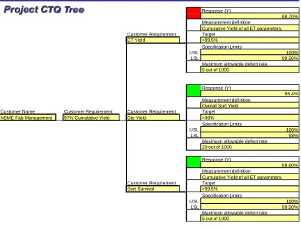
Once the Stakeholder analysis is complete, critical to quality tree map (Figure
3.0.4) would be necessary in order to understand the input parameters which control the
CTQ parameters. If one defines the cumulative yield as the product of ET Yield, Die
Yield and Sort Survival yields, Figure 3.0.4 shows that the ET yield is the only
component which is not hitting the target yield goal. From this analysis, one must focus
Response (Y)
98.70% Measurement definition
Cumulative Yield of all ET parameters. Customer Requirement Target
ET Yield >99.5%
Specification Limits
USL 100%
LSL 99.50%
Maximum allowable defect rate 5 out of 1000
Response (Y)
98.4% Measurement definition
Overall Sort Yield Customer Name Customer Requirement Customer Requirement Target NSME Fab Management 97% Cumulative Yield Die Yield >98%
Specification Limits
USL 100%
LSL 98%
Maximum allowable defect rate 20 out of 1000
Response (Y)
99.60% Measurement definition
Cumulative Yield of all ET parameters. Customer Requirement Target
Sort Survival >99.5%
Specification Limits
USL 100%
LSL 99.50%
[image:46.612.109.541.79.408.2]Maximum allowable defect rate 5 out of 1000
Figure 3.0.4: CTQ Tree
Going after the ET yield became apparent in order to reach the 97% cumulative
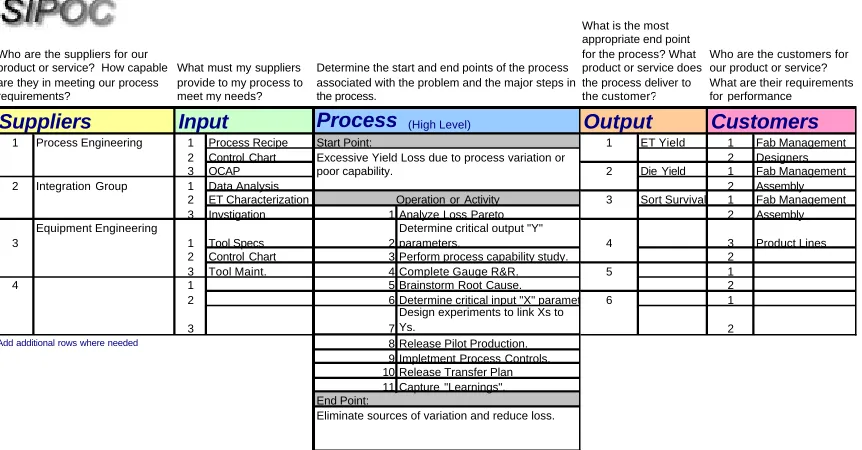
yield goal however the high level process map along with SIPOC needs to get generated
in order to understand the suppliers and the customer relationship. SIPOC is often times
useful in a team setting to get support from every organization in order to successfully
accomplish the team goals. This project requires the input from the integration, process
and equipment engineering groups to execute the high level process to deliver the
customers their required outputs as highlighted in Figure 3.0.5. Process map starts by
identifying the loss Pareto for the ET yields loss. Process capability analysis as well as
Design of experiments are run to determine or to verify the relationship before
[image:47.612.111.542.145.370.2]implementing control charts.
Figure 3.0.5: Supplier, Input, Process, Output, Customer Chart (SIPOC).
3.1 Measure
Measure step helps determine the areas of loss and establish a process capability.
Often time visual analysis as well as understanding the measurement methodologies are
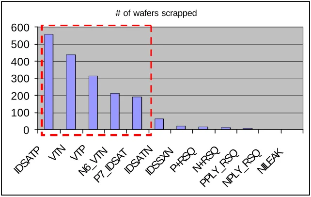
studied. Figure 3.1.0 outlines the number of scrap wafers as a result of the ET parameter
failures. 93% of the total wafer scraps are as a result of the top five ET parameters as
highlighted in Figure 3.1.0. Electrical testing is performed on the scribe-street test
structures between two product die as shown on Figure 3.1.1. Scribe-street test structures
allows product wafers to be screened without impacting the die size.
Suppliers Input Process (High Level) Output Customers
1 1 Process Recipe Start Point: 1 ET Yield 1 Fab Management 2 Control Chart 2 Designers 3 OCAP 2 Die Yield 1 Fab Management
2 1 Data Analysis 2 Assembly
2 ET Characterization 3 Sort Survival 1 Fab Management 3 Invstigation 1 Analyze Loss Pareto 2 Assembly 3 1 Tool Specs 2
Determine critical output "Y"
parameters. 4 3 Product Lines 2 Control Chart 3 Perform process capability study. 2
3 Tool Maint. 4 Complete Gauge R&R. 5 1 4 1 5 Brainstorm Root Cause. 2 2 6 Determine critical input "X" parameters. 6 1
3 7
Design experiments to link Xs to
Ys. 2
Add additional rows where needed 8 Release Pilot Production. 9 Impletment Process Controls. 10 Release Transfer Plan 11 Capture "Learnings". End Point:
Equipment Engineering
Eliminate sources of variation and reduce loss. Process Engineering
Excessive Yield Loss due to process variation or poor capability.
Integration Group
Operation or Activity Who are the suppliers for our
product or service? How capable are they in meeting our process requirements?
What must my suppliers provide to my process to meet my needs?
What is the most appropriate end point for the process? What product or service does the process deliver to the customer?
Who are the customers for our product or service? What are their requirements for performance Determine the start and end points of the process
Figure 3.1.0: ET Loss Pareto
Figure 3.1.1: ET Scribe-street test structures.
It is important to review and understand the electrical test methodologies for the
top five problematic ET parameters.
Linear VT Test conditions for the NMOS transistor is as follows:
D: 0.1 V, compliance 10 mA.
S: 0 V, compliance 10 mA.
G: 0 to 1.8 V, compliance 10 mA. (Ramp)
PW Sub: 0 V, compliance 10 mA.
# of wafers scrapped
0 100 200 300 400 500 600
IDSATP
VTN VTP N6_VTN
P7_IDSATIDSATNIDSSXNP
+RSQN+RSQ
PPLY_RSQNPLY_RSQ NILE
Gate voltage is ramped up from 0V. to 1.8V while keeping the drain voltage at
0.1V and measuring the drain current. Maximum slope point of VG vs. ID curve is
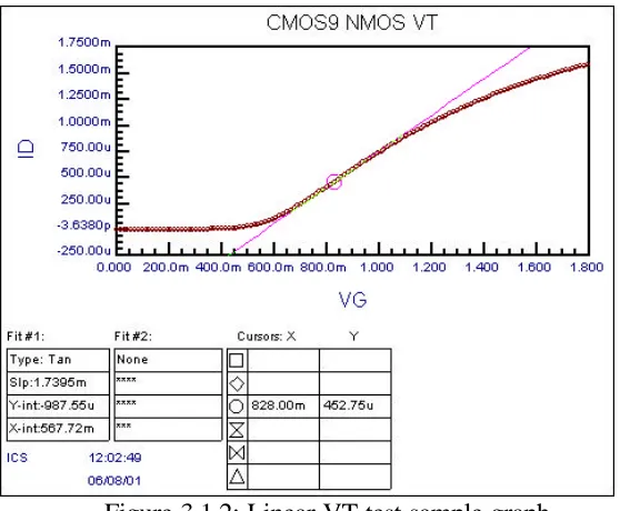
measured as shown on Figure 3.1.2. x-axis intersect of the tangent line at the maximum
slope is me asured. 50 mV (half of drain voltage) is subtracted from the x-axis intercept to
[image:49.612.175.454.372.602.2]calculate the linear threshold voltage. Note that the VTLIN is 0.517V (0.567-0.050) from
Figure 3.1.2. For high voltage NMOS transistor, the VG is ramped from 0V. to 3.3V. In
order to test the PMOS threshold voltage the polarity of the applied voltages are switched
from positive to negative and the appropriate gate voltage is applied as necessary.
Appropriate compliance values need to be set in order to avoid tester or transistor damage
due to unexpected factors.
Figure 3.1.2: Linear VT test sample graph.
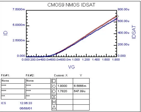
Drain current is measured at the fully saturated threshold point such as maximum
VG and VD values. Test conditions for the NMOS saturation current is as follows.
S: 0 V, compliance 10 mA.
G: 0 to 1.8 V, compliance 10 mA.
PW Sub: 0 V, compliance 10 mA .
Drain and the gate voltages are ramped together as described above. Drain current
is measured at VG=VD= 1.8V and divided by the width of the transistor of 10um in order
to calculate the normalized saturation current. 647uA/um of normalized saturated drain
current is calculated from 6.47mA of measured drain current from Figure 3.1.3. As in the
cause of VT, the gate and drain bias voltages are increased to 3.3V for high voltage
transistors and the polarities are switched to negative for PMOS transistors.
[image:50.612.184.472.332.562.2]
Figure 3.1.3: Fully saturated drain current measurement.
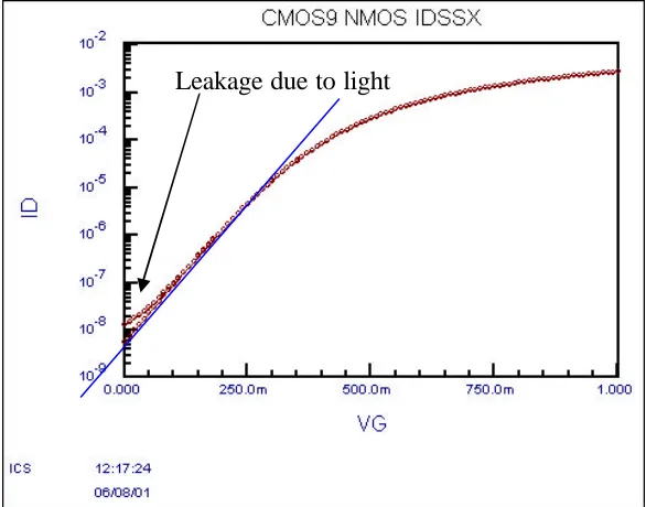
Even though the loss Pareto does not involve any leakage parameters, it is
important to note the measurement method and also study these parameters through out
this project. Leakage test is performed by applying the below bias conditions outlined
D: 2 V, compliance 20 mA.
S: 0 V, compliance 20 mA.
G: 0 to 1 V, compliance 20 mA.
PW Sub: 0 V, compliance 20 mA.
Leakage value is measured at the maximum slope of the VG vs. ID curve. y-axis
intercept of the tangent line at VG=0V is noted as the leakage measurement. This method
allows more accurate testing as a result of tested, probe card or environment noise.
Without the extrapolation method, the presence of light could impact the leakage values
at no gate bias as shown on Figure 3.1.4. High voltage transistors use a drain bias of 3.5V
with the same gate bias. Polarity for the PMOS transistor testing is also reversed during
[image:51.612.174.467.414.644.2]leakage testing.
As discussed earlier, it is important to understand the baseline process capability
of all interested ET parameters. In order to be consistent with the previous discussions,
the Cp and CpK metrics are used in order to compare the process capability as shown on
formulas (17) and (18) [11].
Based on the Cp and CpK performance, three different zones are determined.
Danger (RED) zone with Cp or CpK values <0.8, Moderate (YELLOW) zone with values
[image:52.612.103.531.347.673.2]between 0.8 and 1 and a comfort zone (GREEN) of values >1.
Figure 3.1.5: (a) VTN distribution, (b) VTP distribution. VTP
Mean -0.4474
Std Dev 0.0276
N 1408
CP 0.846
CPK 0.816
Lower Spec Limit -0.52 Upper Spec Limit -0.38 Portion % Actual Below LSL 1.6335 Above USL 0.2131
VTN
Mean 0.500 Std Dev 0.016
N 1408
CP 1.458
CPK 0.409
Lower Spec Limit 0.38 Upper Spec Limit 0.52 Portion % Actual Below LSL 0 Above USL 9.9432
CP/CPK <0.8 >0.8, <1 >1
3s
LSL)]
X
(
),
X
Min[(USL
C
pk=
−
−
(18)3s
LSL)]
X
(
),
X
Min[(USL
C
pk=
−
−
(18)6s
LSL
USL
C
p=
−
(17)6s
LSL
USL
C
p=
−
(17)As seen from the Figure 3.1.5 (a), the VTN distribution CP value is fairly high
however with a poor CpK of only 0.409. Shifting the VTN distribution without impacting
the standard deviation would be enough to increase the overall process capability. Same
is not true for the VTP seen on Figure 3.1.5 (b), where both the shift in mean and
[image:53.612.105.545.214.527.2]tightening of the sigma would be necessary.
Figure 3.1.6: (a) N6_VTX distribution, (b) P7_VTX distribution.
High voltage NMOS VT (N6_VTX) distribution could use re-targeting as well as
the tightening of the overall distribution as seen on Figure 3.1.6(a). Based on the CpK
value of 0.482, targeting the distribution appears to be more urgent. High voltage PMOS
VT (P7_VTX) appears to perform fairly well with both Cp and CpK values above 1.0
(Figure 3.1.6(b)).
N6_VTX
Mean 0.594 Std Dev 0.039
N 1409
CP 0.858
CPK 0.482
Lower Spec Limit 0.45 Upper Spec Limit 0.65 Portion % Actual Below LSL 0 Above USL 11.2846
P7_VTX
Mean -0.644 Std Dev 0.028
N 1408
CP 1.187
CPK 1.119
Lower Spec Limit -0.75 Upper Spec Limit -0.55 Portion % Actual Below LSL 0.071 Above USL 0
CP/CPK
<0.8 >0.8, <1
>1
NMOS saturation current distribution shown on Figure 3.1.7(a) appears to be a
capable parameter. On the other hand, IDSATP CpK of 0.544 show a very incapable
process with a lot Cp as well (Figure 3.1.7(b)) IDSATP mean and sigma needs to be
[image:54.612.113.543.194.505.2]improved in order to achieve a capable process.
Figure 3.1.7: (a) IDSATN distribution, (b) IDSATP distribution.
Both high voltage NMOS and PMOS saturation current process capability appears
to be in good shape although the PMOS saturation current shown in Figure 3.1.8(b) could
benefit from variation reduction.
IDSATN
Mean 618.3 Std Dev 21.2
N 1409
CP 1.417
CPK 1.129
Lower Spec Limit 510 Upper Spec Limit 690 Portion % Actual Below LSL 0 Above USL 0.1419
IDSATP
Mean 314.5 Std Dev 27.9
N 1408
CP 0.836
CPK 0.544
Lower Spec Limit 220 Upper Spec Limit 360 Portion % Actual Below LSL 0 Above USL 3.5511
CP/CPK <0.8
>0.8, <1
>1
Figure 3.1.8: (a) N6_IDSAT distribution, (b) P7_IDSAT distribution.
Log of the leakage measurements were taken in attempt to display a more
normalized distribution. Overall, the leakage current process capability as shown in
Figures 3.1.9 and 3.1.10 is in pretty good health however

![Figure: 3.0.2: Six Sigma DMAIC Process [14].](https://thumb-us.123doks.com/thumbv2/123dok_us/122209.11843/43.612.112.538.85.372/figure-six-sigma-dmaic-process.webp)