RIT Scholar Works
Theses
5-2018
Additive Manufactured Microstructures and
Designs for High Heat Flux Dissipation During
Pool Boiling
Austin Hayes
[email protected]Follow this and additional works at:
https://scholarworks.rit.edu/theses
This Thesis is brought to you for free and open access by RIT Scholar Works. It has been accepted for inclusion in Theses by an authorized administrator of RIT Scholar Works. For more information, please [email protected].
Recommended Citation
Additive Manufactured Microstructures
and Designs for High Heat Flux
Dissipation During Pool Boiling
By
Austin Hayes
A Thesis Submitted in Partial Fulfillment of the Requirements for the Degree of
Master of Science in Mechanical Engineering
Committee Approval
Approved: Date:
Dr. Satish G. Kandlikar
Department of Mechanical Engineering
(Thesis Chair)
Approved: Date:
Dr. Michael Schrlau
Department of Mechanical Engineering
(Department Representative)
Approved: Date:
Dr. Denis Cormier
Department of Industrial Engineering
(Examiner)
Approved: Date:
Dr. Alfonso Fuentes-Aznar
Department of Mechanical Engineering
(Examiner)
Approved: Date:
Dr. Agamemnon Crassidis
Department of Mechanical Engineering
(Examiner)
Additive Manufactured Microstructures
and Designs for High Heat Flux
Dissipation During Pool Boiling
By
Austin Hayes
A Thesis Submitted in Partial Fulfillment of the Requirements for the Degree of
Master of Science in Mechanical Engineering
Department of Mechanical Engineering
Kate Gleason College of Engineering
Rochester Institute of Technology
Rochester, New York 14623
May 2018
Abstract
Masters of Science
by Austin Hayes
Heat dissipation is vital in industries requiring predictable operating temperatures while
also producing large heat fluxes. These industries include electronics and power
gen-eration. For electronics, as more devices fit on a smaller area, the heat flux increases
dramatically. Pool boiling offers a solution to electronic cooling due to extremely high
heat transfer with a low temperature change. Previous research has focused on coatings
and precision manufacturing to create microchannels and features for boiling
augmen-tation. However, this is limited to designs for subtractive processes. The use of additive
manufacturing (AM) offers a novel way of thinking of design for boiling enhancement.
3-D boiling structures are fabricated out of aluminum using the Vader System’s
magneto-jet printer. Three generations of geometric structures are created: a volcano-with-holes,
a miniaturized volcano-with-holes, and a modular volcano-with-holes. These designs are
not easily manufactured using standard techniques. As such, three-dimensional bubble
dynamics are currently being explored using high speed imaging and particle image
ve-locimetry. By printing a volcano shape with base holes, the liquid and vapor phases are
physically separated in a process termed macroscale liquid-vapor pathways.
The singular volcano-with-holes chips achieved a maximum heat flux of 217.3 W/cm2
with a maximum heat transfer coefficient (HTC) of 97.2 kW/m2K (81% improvement
over plain). By producing four volcanoes on a single chip, the liquid flow length inside
the volcano, which acts as the entrance length, is reduced by 25% and the HTC greatly
increased. The highest performing miniaturized volcano-with-holes chip reached a
maxi-mum heat flux of 223.1W/cm2with a maximum HTC of 139.1kW/m2K(150%
improve-ment over plain). Additionally, the highest performing miniaturized chip was printed
on top of a microchannel array. This resulted in combined enhancement from both
mi-crochannel and bubble dynamics resulting in a maximum heat flux of 228.4W/cm2 with
a HTC of 339.6kW/m2K(533% improvement over plain). Finally, a modular structure
was created to determine the individual influence of conduction and bubble dynamic
augmentation on boiling enhancement. The modular designs show an 83% improvement
in CHF (202.4 W/cm2) over plain copper chips and a 83% improvement in HTC(139.0
kW/m2K). This indicates boiling enhancement arises from three-dimensional control
First and foremost, I would like to thank Dr. Satish Kandlikar for welcoming me into the
lab as a freshman looking to do research during a break. This has snowballed into where
I am today and I owe a lot of my academic and professional success to Dr. Kandlikar’s
guidance and support. His love and excitement for his research is truly contagious.
Thank you for always being willing to take a minute to talk to me.
Instrumental to this work was the expertise and knowledge provided by the ME machine
shop experts Rob Kraynik, Craig Arnold, and Rick Wurzer. Thank you for being willing
to help me find a way to do every unusual idea I came in with. Additionally, thank you
to Bill Finch for his countless stories and laughs as well as willingness to help wherever
possible. I would also like to thank my advisor Hillary McCormick for her support and
smile throughout my 5 years here. Along with Hillary, thank you to Jill Ehmann and
everyone else in the ME office who always greeted me with a warm smile.
I would also like to thank my committee members (Dr. Satish Kandlikar, Dr. Michael
Schrlau, Dr. Denis Cormier, Dr. Alfonso Fuentes-Aznar, and Dr. Agamemnon
Cras-sidis) for their help from my proposal to defense. Thank you for your constructive
feedback and help in defining my thesis. I’d like to thank Dr. Ron Aman for first
in-troducing me to the world of additive manufacturing. Thank you to Dr. Cormier for
allowing me to use the Vader System and for providing the expertise of the AMPrint
center for my work. This has been instrumental in helping me decide my focus area for
my PhD and prove my love for research.
Thank you to everyone in my lab who I have been able to fall back on whenever I
had questions. They have been more than willing to take the time to stop and help at
every occasion. Thank you to Alyssa Recinella, Pruthvik Raghupathi, Arvind Jaikumar,
Ankit Kalani, and Aranya Chauhan for their laughs, help, and support.
I would also like to thank my friends who through their smiles, hugs, and love have been
a blessing in my life. I cherish each and every one of you; and the most meaningful
moments of my time at RIT has been the opportunity to get to know you.
Lastly I would like to thank my family for helping shape me into the person I am today.
Thank you to Mom and Dad who have worked to support me from day 1. And of course
thank you to Brandon Hayes for always being my “plus one,” as well as providing your
help in the PIV codes and idea bouncing.
Contents
Committee Approval i
Title Page ii
Abstract iii
Acknowledgements iv
List of Figures vii
List of Tables x
Abbreviations xi
1 Introduction 1
1.1 Pool Boiling Fundamentals . . . 2
1.1.1 Single Phase Convection . . . 3
1.1.2 Nucleate Boiling . . . 4
1.1.3 Transition Boiling . . . 4
1.1.4 Film Boiling . . . 5
1.1.5 Surface Microstructure Enhancement. . . 5
1.2 Additive Manufacturing . . . 6
1.3 Metal Additive Manufacturing . . . 6
1.3.1 Direct Metal Laser Sintering (DMLS) . . . 7
1.3.2 Laser Engineered Net Shaping (LENS) . . . 8
1.3.3 Electron Beam Melting . . . 9
1.3.4 MagnetoJet Printing . . . 10
2 Literature Review 12 2.1 Microchannel Boiling Enhancement. . . 12
2.2 Influence of Surface Roughness . . . 13
2.3 Porosity Heat Transfer Enhancement . . . 15
2.4 Bubble Dynamics on CHF and HTC . . . 15
2.5 Additive Manufacturing Microstructures . . . 17
2.6 Scope of Work . . . 19
3 Experimental Work 22
3.1 Pool Boiling Setup . . . 22
3.2 High Speed Visualization . . . 24
3.3 AM: Vader System . . . 24
3.3.1 Zeroing Vader System . . . 25
3.3.2 Vader System Key Parameters . . . 26
3.3.3 Adhesion Theory . . . 27
4 Results 35 4.1 Uncertainty Analysis–Heat Flux . . . 35
4.2 Vader System - Process Parameters. . . 36
4.3 Vader System - Manufactured Chips . . . 39
4.4 Initial AM Chip Performance . . . 39
4.4.1 Angled Fin . . . 39
4.4.2 Miniaturized Volcano Array . . . 42
4.5 Macroscale Separate Liquid Vapor Pathways . . . 46
4.5.1 Volcano-with-Holes . . . 46
4.5.1.1 Variable Inner Diameter. . . 48
4.5.1.2 High Height . . . 54
4.5.1.3 1 Inlet 1 Outlet . . . 57
4.5.1.4 Repeatability . . . 60
4.5.2 Miniaturized Volcano-with-Holes . . . 61
4.5.2.1 Variable Inner Diameter. . . 63
4.5.2.2 Integrated on Microchannel Surface . . . 66
4.6 Modular Boiling Surface Enhancement . . . 68
5 Conclusions 74
6 Future Work 78
List of Figures
1.1 GENERIC POOL BOILING CURVE [1] . . . 3
1.2 AM MICROSTRUCTURE SURFACE ENHANCEMENT . . . 6
1.3 DIRECT METAL LASER SINTERING MACHINE [2] . . . 8
1.4 LASER ENGINEERED NET SHAPING SCHEMATIC [3] . . . 8
1.5 ELECTRON BEAM MELTING SCHEMATIC [4] . . . 9
1.6 MAGNETOJET PRINTING SCHEMATIC [5] . . . 11
2.1 INCLINED MICROCHANNEL CREATED BY EDM [6] . . . 14
2.2 INLFUENCE OF SURFACE ROUGHNESS ON POOL BOILING OF FC-77 [7] . . . 14
2.3 SEPARATE LIQUID VAPOR PATHWAYS IN MICROCHANNEL EN-HANCEMENT [8] . . . 16
2.4 SEPARATE LIQUID-VAPOR PATHWAYS SELECTIVELY SINTERED MICROCHANNELS [9] . . . 16
2.5 CONTOURED FIN BUBBLE DYNAMICS [10]. . . 17
2.6 MICRO-CAVITY ARRAY CREATED USING SLS [11] . . . 18
2.7 LATTICE STRUCTURES FOR POOL BOILING ENHANCEMENT A). LATTICE UNIT CELL B). EXAMPLES OF REPEATED UNIT CELL [12] . . . 19
3.1 POOL BOILING EXPERIMENTAL SET-UP . . . 23
3.2 TEST CHIP THERMOCOUPLE PLACEMENT . . . 24
3.3 VADER MAGNETOJET PRINTER SCHEMATIC. . . 25
3.4 VADER CHIP FIXTURE - TOP . . . 26
3.5 VADER CHIP FIXTURE - BOTTOM . . . 26
3.6 VADER DROPLET IMPINGEMENT SCHEMATIC . . . 30
3.7 DROPLET IMPINGEMENT SIMULATION DOMAIN . . . 32
3.8 TEMPERATURE CONTOURS AT 3.21 ms AFTER IMPINGEMENT . 33 3.9 TEMPERATURE CONTOURS AT 4.065 ms AFTER IMPINGEMENT . 34 3.10 TEMPERATURE CONTOURS AT 6.27 ms AFTER IMPINGEMENT . 34 4.1 UNCERTAINTY ANALYSIS FOR A PLAIN Al CHIP. . . 37
4.2 Slic3r NOZZLE DIAMETER SET TO 0.78 mm. . . 38
4.3 Slic3r NOZZLE DIAMETER SET TO 0.10 mm. . . 38
4.4 VADER SYSTEM CHIP DESIGNS . . . 39
4.5 ANGLED PILLAR SCHEMATIC . . . 40
4.6 ANGLED PILLAR BUBBLE DYNAMICS . . . 40
4.7 ANGLED PILLAR HIGH SPEED IMAGES SHOWING BUBBLE TRA-JECTORY . . . 41
4.8 ANGLED PILLAR POOL BOILING CURVE . . . 41
4.9 ANGLED PILLAR HEAT TRANSFER COEFFICIENT. . . 42
4.10 MINIATURIZED VOLCANO ARRAY DIMENSIONS . . . 43
4.11 MINIATURIZED VOLCANO BUBBLE DYNAMIC SCHEMATIC . . . . 44
4.12 MINIATURIZED VOLCANO HIGH SPEED IMAGES SHOWING BUB-BLE GROWTH . . . 44
4.13 MINIATURIZED VOLCANO POOL BOILING CURVE. . . 45
4.14 MINIATURIZED VOLCANO HEAT TRANSFER COEFFICIENT. . . . 45
4.15 VOLCANO-WITH-HOLES SCHEMATIC . . . 46
4.16 ACTUAL IMAGES OF PRINTED CHIPS . . . 47
4.17 VOLCANO-WITH-HOLES VARIABLE INNER DIAMETER POOL BOIL-ING CURVE . . . 49
4.18 VOLCANO-WITH-HOLES VARIABLE INNER DIAMETER HTC . . . 49
4.19 MACROSCALE SEPARATE L-V PATHWAY OPTION 1 . . . 50
4.20 MACROSCALE SEPARATE L-V PATHWAY OPTION 2 . . . 51
4.21 CHIP 1 BASE LIQUID SUCTION AT 6.0W/cm2 . . . 52
4.22 CHIP 1 TOP LIQUID SUCTION AT 20.1W/cm2 . . . 52
4.23 PIV BOTTOM CHIP 1 PATHWAY OPTION 1. . . 53
4.24 PIV TOP CHIP 1 PATHWAY OPTION 1 . . . 53
4.25 CHIP 3 BOTTOM LIQUID SUCTION AT 9.5W/cm2 . . . 54
4.26 CHIP 3 TOP VAPOR EXHAUSTION AT 9.5W/cm2 . . . 54
4.27 PIV TOP CHIP 2 PATHWAY OPTION 2 . . . 55
4.28 PIV BOTTOM CHIP 2 PATHWAY OPTION 2. . . 55
4.29 BOILING CURVE OF HIGH HEIGHT CHIP . . . 56
4.30 HTC OF HIGH HEIGHT CHIP . . . 56
4.31 CHIP 4 BOTTOM LIQUID SUCTION AT 8.4W/cm2 . . . 57
4.32 CHIP 4 TOP VAPOR PLUME EXHAUSTION AT 8.4W/cm2 . . . 57
4.33 BOILING CURVE OF 1 INLET 1 OUTLET CHIP. . . 58
4.34 HTC OF 1 INLET 1 OUTLET CHIP . . . 59
4.35 CHIP 5 BOTTOM LIQUID SUCTION AT 11.4W/cm2 . . . 59
4.36 CHIP 5 TOP VAPOR EXHAUSTION AT 11.4W/cm2 . . . 59
4.37 PIV ANALYSIS OF 1 INLET 1 OUTLET SHOWING PATHWAY OP-TION 2 (SIDE VIEW) . . . 60
4.38 REPEATABILITY BOILING CURVE FOR CHIP 1 . . . 61
4.39 REPEATABILITY HTC FOR CHIP 1 . . . 61
4.40 MINIATURIZED VOLCANO-WITH-HOLES SCHEMATIC. . . 62
4.41 MINIATURIZED VOLCANO-WITH-HOLES ACTUAL CHIP IMAGES . 63 4.42 MINIATURIZED VOLCANO-WITH-HOLES POOL BOILING CURVE . 64 4.43 MINIATURIZED VOLCANO-WITH-HOLES HTC. . . 65
4.44 CHIP 6 BOTTOM LIQUID SUCTION AT 10.1W/cm2 . . . 65
4.45 CHIP 6 TOP LIQUID INLET AT 10.1W/cm2 . . . 65
4.46 CHIP 8 BOTTOM LIQUID SUCTION AT 11.0W/cm2 . . . 66
4.47 CHIP 8 TOP VAPOR EXHAUSTION AT 11.0W/cm2 . . . 66
4.48 MINIATURIZED VOLCANO-WITH-HOLES ON MICROCHANNEL . . 67
List of Figures ix
4.50 BEST PERFORMING ADDITIVE MANUFACTURED STRUCTURES: HTC . . . 68
4.51 MODULAR SURFACE FIXED WITH KAPTON TAPE (CHIP 10) . . . 69
4.52 MODULAR SURFACE FIXED WITH KAPTON TAPE (CHIP 11) . . . 70
4.53 MODULAR ACTUAL CHIP IMAGES. . . 70
4.54 MODULAR VOLCANO-WITH-HOLES ON COPPER BOILING CURVE 71
4.55 MODULAR VOLCANO-WITH-HOLES ON COPPER HTC . . . 72
4.56 CHIP 10 MODULAR BOTTOM LIQUID SUCTION AT 10.9W/cm2 . . 72
1.1 APPROXIMATE HEAT TRANSFER COEFFICIENTS FOR CONVEC-TIVE MODES [13] . . . 2
1.2 ADVANTAGES AND DISADVANTAGES OF DIRECT METAL LASER SINTERING . . . 7
1.3 ADVANTAGES AND DISADVANTAGES OF LASER ENGINEERED NET SHAPING . . . 9
1.4 ADVANTAGES AND DISADVANTAGES OF ELECTRON BEAM MELT-ING . . . 10
1.5 ADVANTAGES AND DISADVANTAGES OF MAGNETOJET PRINT-ING . . . 10
2.1 SUMMARY OF BOILING ENHANCEMENT FROM LITERATURE . . 21
3.1 VADER DROPLET ADHESION THEORY PARAMETERS . . . 29
3.2 MATERIAL PROPERTIES FOR ALUMINUM 4043 (WELDING WIRE) 31
4.1 SYSTEMATIC UNCERTAINTY . . . 36
4.2 VOLCANO-WITH-HOLES TEST CHIP DESCRIPTIONS . . . 47
4.3 VOLCANO-WITH-HOLES TEST CHIP DIMENSIONS . . . 48
4.4 MINIATURIZED VOLCANO-WITH-HOLES TEST CHIP DESCRIP-TIONS. . . 62
4.5 MINIATURIZED VOLCANO-WITH-HOLES TEST CHIP DIMENSIONS 63
4.6 MODULAR SURFACE ENHANCEMENT CHIP DESCRIPTIONS . . . 70
4.7 MODULAR SURFACE ENHANCEMENT CHIP DIMENSIONS . . . 71
5.1 AM CHIP RESULTS. . . 77
Abbreviations
DMLS DirectMetal Laser Sintering
LENS Laser EngineeredNetShaping
AM Additive Manufacturing
CHF CriticalHeatFlux
HTC HeatTransfer Coefficient
Introduction
Advances in microelectronics have resulted in manufacturing silicon chips with
con-tinually smaller transistors. This improved computing performance is associated with
the ability to pack more electronics in a given area. From a thermal perspective, an
increased transistor count requires a need to dissipate extra generated heat. In
conjunc-tion, a smaller component area results in significantly higher heat fluxes. Therefore,
there is need from the electronics industry to improve the thermal management ability
of electronic components. Current cooling practices include fan and liquid set-ups, both
relying on sensible heat as no phase change occurs. Fan-based cooling requires a large
power input thereby increasing power consumption of an electronic system. Although
capable of removing large quantities of heat, liquid cooling requires careful attention to
seals in order to contain the working fluid and may require chilled water to discharge the
heat. Boiling is promising for electronic cooling due to its high heat transfer coefficients
with low increase of the working fluids temperature. Boiling takes advantage of a liquid’s
high latent heat which allows for large heat dissipation from a small area as seen in the
electronics industry.
While extensive research in enhanced boiling has been undertaken by the electronic
industry, its application is far-reaching. Looking to power generation, Rankine power
plants operate off of phase change heat transfer from the boiler to the working fluid.
Improving the efficiency of this heat transfer improves the overall system efficiency.
Power generation systems such as natural gas or nuclear power plants rely on boiling
for steam generation and temperature regulation. Specifically, nuclear power plants
2
must remain within specific temperature bounds to prevent catastrophic failure. Thus,
a large factor of safety exists to ensure the boiling process does not reach its critical
limit. Microstructure enhancements have the potential to increase this critical limit
providing greater generation capacity. Furthermore, air conditioning and refrigeration
units all employ phase change as the mechanism to remove sensible heat from the air
through the latent heat of the working refrigerant. Boiling heat transfer forms the
underlying physics of all of these systems and microstructure enhancement is identified
as a promising technique for heat transfer augmentation.
1.1
Pool Boiling Fundamentals
Boiling is separated into two main categories: pool boiling and flow boiling. Pool boiling
explores buoyancy-driven bubble dynamics resulting from submerging a heated surface
in a liquid. The study of pool boiling on planar geometries holds promise for improving
thermal management. This is because of the high heat transfer coefficients attainable
through pool boiling. The heat transfer coefficient for various thermal management
techniques can be seen in Table1.1
Table 1.1: APPROXIMATE HEAT TRANSFER COEFFICIENTS FOR CONVEC-TIVE MODES [13]
Process Fluid Heat transfer coefficient [mKW ]
Free Convection Liquids 2-25
Free Convection Gases 50-1,000
Forced Convection Liquids 100-20,000
Pool Boiling Liquids 1,000-150,000
Pool boiling is characterized by no external bulk motion of liquid. In other words,
boiling occurs without a pump and no external work is applied to the system. At the
interface between the heated surface and liquid, convective currents begin due to density
differences as the fluid warms. At high magnifications, all surfaces exhibit cavities. At
high enough heat fluxes, these cavities nucleate and bubbles grow from within the cavity
both due to inertial and thermal modes. Within the field of boiling, one of the most
Figure 1.1: GENERIC POOL BOILING CURVE [1]
produced through heat flux or temperature controlled experiments. However, more often
than not due to ease of experimentation a heat flux controlled mechanism is employed.
The heat flux,q00, is the dependent variable and depicts the amount of heat per unit area
(W/m2). The wall superheat is the difference between the liquid saturation temperature
and the bulk liquid temperature (K). There are four main divisions of the pool boiling
curve: single phase convection, nucleate boiling, transition boiling, and film boiling. A
generic pool boiling curve is seen in Figure1.1.
1.1.1 Single Phase Convection
As the surface temperature rises above the saturation temperature, heat transfer by
natural convection takes place. At this point, nucleation does not occur and an
ap-proximately linear line is seen on the pool boiling curve as defined by Newton’s Law of
Cooling dq
00
dt =h(T(t)−Tenv). Minimal sub-cooled boiling may be achieved; however,
the cavities are not nucleating. Any bubbles forming are localized to specific areas of
4
1.1.2 Nucleate Boiling
At sufficient heat flux, the cavities on the heater surface begin to nucleate. This point
is characterized by a significantly steeper slope on the pool boiling curve, indicative of
a much higher heat transfer coefficient. In the initial stages of nucleate boiling, heat
transfer at the solid-liquid interface is large enough for some nucleation, yet the cooler
bulk fluid prevents it from happening fully. This is referred to as sub-cooled boiling. As
bubbles separate and collapse into the fluid they introduce fluid mixing and convective
currents which increase q00 and HTC. As the bulk fluid reaches the saturation
temper-ature, full nucleate boiling ensues. With increasing heat flux, a greater range of cavity
radii begin to nucleate. The advantage of pool boiling for heat transfer lies in its high
heat flux at low wall superheat, which is indicative of high heat transfer coefficients. At
the inflection point, bubbles begin to coalesce into vapor slugs or jets which interfere
with liquid re-wetting resulting in diminished heat transfer. At the Critical Heat Flux
(CHF), the point denoted by QCHF, violent boiling produces large amounts of vapor
which forms a vapor layer across the heated surface. This vapor blanket inhibits liquid
re-wetting and the dominant heat transfer mechanism is conduction through the vapor
layer. As a result, the heat transfer coefficient dramatically drops which leads to
ex-tremely high temperature spikes on the order of 100K/sec for water. This oftentimes
leads to system failure and therefore value exists in increasing this point. As can be seen
by the pool boiling curve, a higher heat flux with lower wall superheat is indicative of
enhanced boiling heat transfer.
1.1.3 Transition Boiling
In reality, CHF is not a static point. Perhaps the chaotic boiling disrupts the vapor layer
allowing liquid re-wetting for a time, or the vapor film forms and is displaced. However,
after CHF, the vapor blanket becomes more dominant and the liquid is increasingly
unable to re-wet the surface. Heat can only escape through conduction and radiation.
As conduction within a vapor film is poor and radiation requires very high temperatures
for heat transfer, boiling heat transfer decreases substantially at this point. As a result,
1.1.4 Film Boiling
The point of inflection between transition boiling and film boiling is known as the
Lei-denfrost point. At this point the heat flux is at its minimum and a vapor film
com-pletely covers the solid-liquid interface. Solely conduction and radiation govern heat
transfer through the vapor film. The wall superheat increases substantially (≈1,000oC for water). At higher wall superheat temperatures, radiation becomes the dominant
heat transfer mechanism. These extremely high wall superheats make transition and
film boiling undesirable for thermal management. The heated surface temperature may
greatly exceed the melting or glass transition temperature of the boiling set-up resulting
in system failure.
1.1.5 Surface Microstructure Enhancement
By shifting the pool boiling curve to the left (ie: obtaining a higher heat flux with lower
wall superheat), the pool boiling heat transfer coefficient can be greatly augmented. One
way of accomplishing this task is through the addition of microstructures on the heated
surface. These structures are a passive enhancement mechanism without the need of
external pumps, rotation, or agitators. As a result, these passive techniques are prime
areas of research to enhance boiling performance. Conventionally, microstructures take
the form of microchannels which are stamped or CNC engraved into the heated surface.
There are two main theories of enhancement for microchannel-enhanced surfaces. First,
the increase in surface area results in greater area for heat transfer. Second,
microchan-nels provide artificial nucleation sites and preferential nucleation at the bottom of the
channel due to higher temperature, as the bottom of the channel is closer to the heat
source. Because of this preferential nucleation, the bubble dynamics can be controlled
by microchannel placement further improving boiling performance. However, these
mi-crostructures can also be created by additive manufacturing. Instead of engraving a
channel, a fin is built up layer by layer. A schematic of additive manufactured fins is
6
Figure 1.2: AM MICROSTRUCTURE SURFACE ENHANCEMENT
1.2
Additive Manufacturing
Additive manufacturing technology is revolutionary in that it changes the conventional
“design for manufacturing” to a novel “design for functionality” approach. In an additive
approach, a part is built up in a layer-by-layer process with high resolution obtained with
thinner layers. Many manufacturing constraints are removed such as internal
geome-tries, unsupported walls, and internal holes. Furthermore, “complexity is free” meaning
that printing complex parts costs the same and requires the same process as simple
parts. As a result, it is advantageous to push the manufacturing capabilities of additive
manufacturing in order to realize as much functionality benefits as possible. Two main
subdivisions exist within additive manufacturing: polymer and metal printing. This is
an intuitive subdivision as each material requires specific methods to achieve printability.
For polymers this includes steroelithography for photopolymers, fused deposition
mod-eling for amorphous polymers, and laser sintering for crystalline polymers. For metals,
the process is much more complicated due to the need for high temperatures or pressures
to create a solid part. Methods to achieve metal printing oftentimes include a powder
bed where very fine powder on the order of 10−75µm is fused with an energy source.
1.3
Metal Additive Manufacturing
Due to its complexity, a wide number of technologies exist to print metal components.
The complexity of metal printing arises from high melting temperatures of metal. In
order to achieve a solid, dense part, a large amount of energy must be imparted on the
feed stock. For powder based systems, this is done through a laser or electron beam
which provides enough energy to locally melt the metal powder together. Ultrasonic
welding utilizes high frequency ultrasonic waves under heat and pressure to produce a
solid-state bond at temperatures well under the metal’s melting point. Additionally,
a new technology, magnetojet printing, prints liquid metal droplets through high
fre-quency magnetic pulses around a molten metal reservoir. Each technology is evaluated
in terms of its advantages and disadvantages. The machines available at RIT and
se-lected to explore to print microstructures are the Hybrid Manufacturing Technologies
laser cladding system and Vader Systems magnetojet printer.
1.3.1 Direct Metal Laser Sintering (DMLS)
Direct metal laser sintering is a powder based system which uses a high power laser beam
to locally melt metal powder to form a solid part. This is done in an inert atmosphere to
prevent oxidation. As the laser scans across the powder, it creates a localized melt pool
dependent on laser parameters such as beam diameter and power. The scanning process
is a 2D raster scan and after each scanning layer a powder roller feeds an additional
layer of powder. In this way the metal part is built up layer by layer. A schematic of a
DMLS machine can be seen in Fig. 1.3. Furthermore, Table 1.2depicts advantages and
disadvantages of AM manufacturing using DMLS.
Table 1.2: ADVANTAGES AND DISADVANTAGES OF DIRECT METAL LASER SINTERING
Advantages Disadvantages
High complexity Reflective metal difficulty
Higher surface finish in AM Potential anisotropic microstructure
Self supported by powder Slow deposition rate
No need for vacuum atmosphere High thermal stress
Potential lack of fusion Inert atmosphere required
8
Figure 1.3: DIRECT METAL LASER SINTERING MACHINE [2]
1.3.2 Laser Engineered Net Shaping (LENS)
Laser engineered net shaping is similar to DMLS in most areas except for the powder
feeder. A high power laser creates a localized melt pool where powder fuses to form
the part. In a LENS system, the powder feedstock is brought to the focal point of
the laser with an inert carrier gas. As a result, the need for extremely large amounts
of powder is eliminated. Furthermore, this process allows metal alloying and gradient
metal printing by adjusting the mass flow rate of metal powder through multiple powder
feeders. Fig. 1.4 depicts a schematic of the process and Table1.3 identifies advantages
and disadvantages of the process.
[image:20.596.230.401.547.664.2]Table 1.3: ADVANTAGES AND DISADVANTAGES OF LASER ENGINEERED NET SHAPING
Advantages Disadvantages
High complexity Relatively low deposition rates
Lower powder waste Inert atmosphere required
Completely dense parts Large overhangs difficult (no support material)
Can print on 3D surface (repairs) Requires thermal post-processing
Functionally graded materials possible Increased control requirements
1.3.3 Electron Beam Melting
Electron beam melting is a powder bed based technology similar to DMLS that uses
a focused electron beam as the high energy source needed for powder fusion. In this
method, the build chamber is placed under high vacuum. This prevents the electron
particles from colliding with the air and ensures proper delivery to the powder.
Com-puter controlled magnets guide the beam at high speed to locally melt the powder into
a solid metal part. After each layer a powder roller re-coats the build platform and the
electron beam scans again. Electron beam melting boasts greater build rates with lower
energy consumption as it does not occur losses due to reflectivity of the metal. As a
result, a lower power electron beam can achieve powder fusion. Arcam (A part of GE
Additive) dominates the market in EBM machines. A schematic is shown in Fig. 1.5
and advantages and disadvantages in Table1.4.
10
Table 1.4: ADVANTAGES AND DISADVANTAGES OF ELECTRON BEAM MELTING
Advantages Disadvantages
High complexity achievable High vacuum needed
Low powder waste Emits X-ray radiation
Highly dense parts Vacuum and cooling time needed
Low contamination due to vacuum Requires post-processing
Higher deposition rates than DMLS Build chamber size limitations
Low power e-beam (no reflectivity concern)
1.3.4 MagnetoJet Printing
A relatively new technology which began development in 2011 by Vader Systems [14] is
MagnetoJet printing. The underlying physical principle of this technology is that metal
in its molten state will undergo a force when acted upon by a strong, time varying
mag-netic and electric fields. In MagnetoJet printing, metal wire is fed into a reservoir which
is heated above its melting temperature by graphite heaters. Next, a pulsed
electromag-net generates a strong magelectromag-netic field surrounding the molten reservoir. The interaction
between the magnetic and electric fields create a Lorenz force which produces eddy
cur-rents pushing the molten metal down the reservoir. At the bottom of the reservoir is a
small diameter nozzle (500µm). Under the pulsed magnetic field, a droplet is released
from the nozzle. Argon gas is passed within the nozzle to prevent oxidation and
con-trol the firing angle. A stream of molten droplets is produced by pulsing at very high
frequencies which are used to build up a solid, dense metal part. This technology
sub-stantially reduces cost through common metal wire feedstock. The MagnetoJet printing
process can be seen in Fig. 1.6 and advantages and disadvantages seen in Table1.5.
Table 1.5: ADVANTAGES AND DISADVANTAGES OF MAGNETOJET PRINT-ING
Advantages Disadvantages
High complexity achievable Nozzle and reservoir consumables
No metal powder Consistent jetting difficult in beta phase development
High density parts Requires post-processing (machining)
Low cost wire feedstock High deposition rate
Chapter 2
Literature Review
Pool boiling is advantageous to meet the need of high heat transfer in small areas.
Its ability to withstand high heat fluxes with low wall superheats is vital to thermal
management practices. Past research has focused on passive methods to enhance pool
boiling performance. Passive methods are explored as they do not require external work
or system complications and instead rely on understanding of the boiling physics. This
literature review focuses on research into passive enhancement techniques such as
micro-channels, porosity, and bubble dynamics as well as the use of additive manufacturing
for microstructures. Initial work in understanding the boiling process was done by
Nukiyama [1]. By restively heating a nichrome wire, the first pool boiling curve was
created. Nukiyama proposed that a heat flux controlled experiment does not depict the
transition of the pool boiling curve past the critical heat flux. In order to view past
this transition point, he proposed a temperature-controlled experiment. By controlling
the wall superheat, data can be collected past the critical heat flux into the transition
and film boiling region. The completion of the curve was demonstrated by Drew and
Mueller [15].
2.1
Microchannel Boiling Enhancement
Microscale surface enhancements have the potential to greatly increase CHF and
dissi-pated heat fluxes due to improved liquid wetting and nucleation sites. Increasing the
effective surface area leads to higher heat transfer over the test surface. Along with
increased nucleation sites, both mechanisms improve boiling heat transfer. Cooke and
Kandlikar [16] depict a 3.4 times improvement in boiling over plain silicon chips with the
use of microchannel surface enhancements. Altering the size, width, and height of the
channel optimizes liquid-vapor pathways further increasing the heat transfer coefficient.
Cooke and Kandlikar performed a parametric analysis varying the microchannel width,
depth, and fin width to determine best performance. They found best results with a
wider, deeper channel with smaller fin widths [8]. Kwak et al. used [17] MEMS
etch-ing to create microchannels with high aspect ratio (larger depth than width) on silicon.
Through capillary wicking experiments, they found as the microchannel depth increases,
the liquid wicking increases with a consistent capillary pressure gradient. This increased
wicking draws liquid supply to the dry spot after bubble departure resulting in increased
heat transfer. They found a width of 30µmand height of 100µmperformed best reaching
CHF at 250 W/cm2 with a HTC of 60 kW/m2K. A variety of microchannel
geome-tries have been explored by researchers. CNC machining has been used to make square
microchannels and rounded microchannels. Electrical Discharge Machining (EDM) can
be used to create higher aspect ratio channels as well as parabolic, stepped, and incline
channels. Walunj et al. [18] created rectangular, parabolic, and stepped microchannels
using EDM on a copper substrate. All configurations increased boiling heat transfer
with the best performing stepped microchannel structure reaching 180W/cm2 at a wall
superheat of 11.7◦C. By observing bubble departure diameters and high speed imaging,
they postulate the enhancement by stepped microchannel is due to the wider channel
top width improving microlayer evaporation with weaker wall forces. Continuing
geome-tries from EDM, Gheitaghy et al. [6] created inclined microchannels in copper seen in
Fig. 2.1. They explored the effect of channel inclination concluding that enhancement
increases as inclination decreases from 90◦ with maximum enhancement at 45◦. Best
performance with a depth of 1.4mm, fin width of 0.8mm, channel pitch of 0.5mm, and
inclination of 45◦ was CHF at 150 W/cm2 and a 12◦C wall superheat.
2.2
Influence of Surface Roughness
Research into surface roughness indicates that rougher surfaces augment pool boiling.
This mechanism is said to result from increased active nucleation site density due to
14
Figure 2.1: INCLINED MICROCHANNEL CREATED BY EDM [6]
in 2005 [7] using EDM and polishing to create surfaces of increasing roughness. They
found an increase in HTC with increasing surface roughness (Fig. 2.2). Mchale and
Garimella also measured an increased active site frequency for rougher surfaces.
Figure 2.2: INLFUENCE OF SURFACE ROUGHNESS ON POOL BOILING OF FC-77 [7]
One reason for increased performance lies in an increased number of nucleation sites.
Kim et al. [19] created micro-pillars and nano-rods on a silicon surface to control the
roughness of the surface. The micro-pillars were 6 µm high with a 50 µm pitch.
Fur-thermore, they created nano-rods with heights between 800 nm and 900 nm. It was
observed that the nano-rod enhanced surfaces achieved higher CHF than the micro-pillar
surfaces; however, a combination of both exhibited the highest CHF at 2346 kW/m2.
2.3
Porosity Heat Transfer Enhancement
Jaikumar and Kandlikar [20] employed selectively sintered fin tops with a channel width
of 762 µm, channel depth of 400 µm, and fin width of 200 µm to achieve CHF at 313
W/cm2 and a HTC of 565 kW/m2K. Combining microchannels and porous
enhance-ments controls both liquid-vapor wetting pathways and the number of nucleation sites
via porosity. Surface enhancements shift the boiling curve to the left resulting in higher
heat flux dissipation with lower wall superheats. Thiagarajan et al. [21] created
micro-porous surfaces with thicknesses of 100µm, 360µm, and 700µm. HFE-7100 was chosen
as the working fluid due to its low global warming potential and good thermodynamic
properties. Their findings agree with literature in that thicker porous coatings result
in improved HTC. With the 700µm coating thickness they obtained a 270% HTC
im-provement. They postulated this is due to a thicker coating resulting in a larger number
of nucleating sites. However, at high heat fluxes the HTC decreases due to the large
rate of vapor generation preventing liquid return pathways. Sarangi et al. [22] explored
a “free-particle” technique of adhering loose copper particles to a copper test chip. This
method is compared to traditional sintering and they found 95% reduction in wall
super-heat for the sintered chip. Furthermore, a powder size between 90−106µmwas optimal
for both the sintered and “free-particle” approaches. It is postulated that thicker
coat-ings greatly reduce the wall superheat due to an increased number of nucleation sites.
As the coating decreases, the HTC enhancement increases. However, thicker coatings
cause coalescence and hinders bubble departure leading to reduced CHF. In general, as
the sintered coating thickness decreases, CHF decreases. They suggest this may be due
to the reduction in effective heat transfer area having a more dominant effect than the
reduced hydraulic resistance associated with a reduction in coating thickness.
2.4
Bubble Dynamics on CHF and HTC
Cooke and Kandlikar coined the term separate liquid-vapor pathways as a means of
microchannel enhancement [8]. In this mechanism, liquid enters the microchannel from
the side along the cooler top of the fin while nucleation and vapor production primarily
16
Figure 2.3: SEPARATE LIQUID VAPOR PATHWAYS IN MICROCHANNEL EN-HANCEMENT [8]
Jaikumar and Kandlikar [9] continued this work exploring selectively sintered
microchan-nel fin tops and chanmicrochan-nel surfaces to explain the separate L-V pathways. They found
depositing sintered coatings inside narrow channels leaving the fin tops plain established
record CHF at 420 W/cm2 with a wall superheat of only 1.7◦C. Separate liquid-vapor
pathways was identified as the main contributor to enhancement seen in Fig. 2.4.
Figure 2.4: SEPARATE LIQUID-VAPOR PATHWAYS SELECTIVELY SINTERED MICROCHANNELS [9]
A thorough study of this mechanism was undertaken by Kandlikar [23] to isolate the
theory of enhancement. Kandlikar concludes the bubble induced convection around a
bubble creates macroconvection currents as the bubbles depart along a specified
departure bubble diameter). Directing these convection currents allows the incoming
liquid and departing vapor to enhance heat transfer.
As a bubble grows on a flat surface, it experiences a symmetric temperature distribution
in the horizontal direction. However, when this bubble grows from a fin, it experiences
an asymmetric temperature distribution which results in an un-even evaporation
mo-mentum force. Kandlikar [24] first hypothesized this un-balanced force can be used to
control the direction of a nucleating bubble. By controlling its direction, separate
liquid-vapor pathways can be established. Separating the liquid and liquid-vapor streams enhances
boiling through a re-circulation pattern where cool liquid re-wets dry-spots during
bub-ble growth. Raghupathi [10] quantified this evaporation momentum force through a
force balance of a bubble under an asymmetric temperature distribution. He also tested
a contoured fin structure seen in Fig. 2.5to demonstrate the potential of the evaporation
momentum force in creating separate liquid-vapor pathways. With the contoured fin,
he achieved a CHF of 300W/cm2 with a HTC of 629 kW/m2k.
Figure 2.5: CONTOURED FIN BUBBLE DYNAMICS [10]
2.5
Additive Manufacturing Microstructures
The first step in combining additive manufacturing with boiling lies in the ability to
additively create microstructures. Therefore, characterization of the laser process
pro-vides the foundation for researchers to create boiling enhancements. The majority of
literature focuses on laser-based printing methods such as DMLS to create these
mi-crostructures. Agarwala et. al. [25] utilized Direct Laser Sintering to investigate the
18
As the powder size decreases, localized heating increases with the same laser intensity
resulting in quicker layer build times and higher densification. Also, lower particle
diam-eters result in improved surface finishes. Min et al. [26] obtained minimum line widths
of 12µm and heights of 10µm through laser sintering of a copper complex ink. The
low layer height was achieved by spin coating an entire surface and selectively sintering
the desired Copper pattern. However, this approach is only suited for one layer height
microstructures or conductive metallization as spin coating would not work after initial
sintering. Ho et al. [11] utilized selective laser melting to achieve 99% part densification
of aluminum 6061 while controlling fin thickness, porosity, permeability, and pore size.
Their selective laser melting machine used a Yb: YAG laser with maximum power at
400W, a beam spot size of 80µm, and powder diameters of 20-63µm. Advantages of
selective laser melting include combining both sintering and patterning in one process.
Yan et al. [27] depict similar results presenting SLM as a method to obtain objects with
complex geometries and mechanical properties. One of the defining parameters of SLM
is the beam diameter, as large beam diameters lead to difficult control of microstructure
dimensions.
There is limited research in using additive manufacturing for boiling enhancement. This
is due in part to the difficulty in creating microstructures with commercial additive
pro-cesses. Ho et al. [11] used selective laser melting to a create a micro-cavity array of
AlSi10Mg seen in Fig. 2.6. Using FC-72, they found a 70% improvement in HTC and
76% improvement in CHF over a plain aluminum 6061 chip. The proposed enhancement
is due to inherent surface grooves and cavities due to the laser melting process. They
developed a general correlation using the Rohsenow model to predict heat flux.
Contin-Figure 2.6: MICRO-CAVITY ARRAY CREATED USING SLS [11]
uing off of this work, Wong and Leong [12] created an octet-truss lattice unit cell out
of AlSi10Mg powder varying the height and cell size (Fig. 2.7). Heat transfer
capillary-assisted suction due to porosity, and seperate liquid-vapor pathways. The
best performing structure achieved a 181% enhancement in HTC with FC-72. Boiling
structures were created on the macroscale range due to machine limitations. However,
micro-cavities are inherently created due to the sintering process. As a result, unique
liquid-vapor interactions are made possible by the 3-D geometries and enhanced boiling
made possible by the presence of cavities on these structures. It is proposed that a
5mm unit cell achieved the highest CHF (107 W/cm2) due to rapid sustained bubble
evacuation from a larger pore size.
Figure 2.7: LATTICE STRUCTURES FOR POOL BOILING ENHANCEMENT A). LATTICE UNIT CELL B). EXAMPLES OF REPEATED UNIT CELL [12]
2.6
Scope of Work
This work will present the applications of magnetojet printing on fabricating advanced
pool boiling surfaces. This is the first work using the Vader System’s magnetojet printer
for pool boiling applications. Novel geometries are created by understanding the
boil-ing phenomenon and these geometries are tested to prove agreement with a proposed
enhancement theory. Specifically, this thesis contains three major components:
manu-facturing, testing, and visualization and PIV analysis.
1. Manufacturing
Using the first Vader System magnetojet printer, a repeatable process is created
to print aluminum (Al) droplets on top of an aluminum chip. Aluminum was
chosen as the feedstock as the build chamber is not inert and oxidation is limited
on Al. Had copper been used, oxidation would diminish boiling performance.
Additionally, aluminum has a lower melting temperature (660◦C) as compared to
copper (1080◦C). This is important both in the heater temperature needed to melt
20
In addition to printing parameters, there is a need to zero or locate the printed
structures on the chip surface. Specifically, all printed structures much lie within
a 10mm x 10mm area on each chip.
2. Testing and Visualization
Pool boiling tests are performed for each manufactured chip. In this manner,
the pool boiling curve is compared to a plain chip to relate design changes to
performance. A Photrom FASTCAM 1024 PCI camera is used to capture bubble
dynamics and provide evidence for mechanisms of boiling enhancement.
3. PIV Analysis
Particle Image Velocimetry (PIV) is another method of characterizing the
mech-anism of boiling enhancement. By seeding the fluid with particles, the flow field
Chapter 3
Experimental Work
3.1
Pool Boiling Setup
A heat flux driven experimental approach is chosen due to ease of implementation by
means of 400W cartridge heaters and thermocouples. The experimental set-up can be
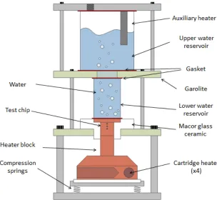
seen in Fig. 3.1. The aluminum test chip lies within the water reservoir and both the
heater and chip are insulated by Macor machinable glass ceramic to reduce heat transfer
losses.
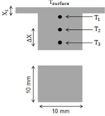
Due to insulation of the aluminum test chip, we assume 1D conduction to determine the
heat flux. From the three thermocouple measurements seen in Fig. 3.2, the heat flux
through the copper heater can be determined. Due to the conservation of energy under
no losses, the heat flux through the copper heater must be equivalent to the heat flux
through the aluminum chip. From the thermocouples, the heat flux is determined by
Fourier’s Law:
q”=−kAl
dT
dx (3.1)
A backwards Taylors series approximation using the three embedded thermocouples is
used to calculates the temperature gradient in the aluminum chip. Assuming negligible
contact resistance, the heat flux through the heater is equal to that passing through the
chip and that at the surface. Therefore:
Figure 3.1: POOL BOILING EXPERIMENTAL SET-UP
dT dx =
3T1−4T2+T3
2∆x (3.2)
The surface temperature was calculated knowing the heat flux and top thermocouple
temperature by:
Tsurface =T1−q”
x1
kAl
(3.3)
WhereT1 is the top thermocouple temperature, q” is the calculated heat flux, x1 is the
distance of the thermocouple location below the chip surface and kAl is the thermal
conductivity. The value ofx1 is equal to 1.7 mm and ∆x is 3 mm. The wall superheat
is given by:
24
Figure 3.2: TEST CHIP THERMOCOUPLE PLACEMENT
3.2
High Speed Visualization
High speed visualization using a Photron FASTCAM 1024 PCI high speed camera is
uti-lized to observe bubble dynamics during boiling. High speed imaging allows liquid and
vapor resupply paths to be observed as well as providing theory for the reason behind
boiling enhancement. Furthermore, individual bubbles can be seen allowing the
rela-tionship between microstructure geometry and bubble trajectory to be experimentally
seen.
3.3
AM: Vader System
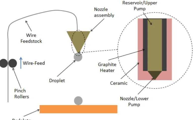
Vader Systems, operated by father and son duo Zack and Scott Vader, is the first
magnetojet molten metal printing system. In collaboration with RIT’s AM Print Center,
the very first delivered machine was sent to RIT during the Summer of 2017. A system
schematic is seen in Fig. 3.3. This system utilizes a metal wire feedstock which is drawn
into a heated reservoir at 950oC. A negative feedback loop controls the amount of molten metal in the reservoir by means of laser measurement. Argon gas flows within the nozzle
assembly to prevent oxidation. To jet or form droplets, an electromagnet placed around
the upper reservoir is pulsed at high frequency to create an oscillating magnet field. This
magnetic field creates a Lorenz force within the nozzle producing eddy currents which
pushes the molten metal to the bottom of the reservoir. The nozzle lines up with the
upper pump/reservoir and has a 500 µm orifice to form the droplet. Under a pulsed
magnetic field controlled by the electromagnet, droplets begin to fire. The bedplate is
controlled by x and y servo motors while the nozzle assembly is constrained to only move
Figure 3.3: VADER MAGNETOJET PRINTER SCHEMATIC
3.3.1 Zeroing Vader System
As with most 3D printers, accuracy and repeatable part placement is difficult. The
Vader System was meant to print parts directly on the build plate; however, since
the machine uses CNC machine stages, it has precise x,y, and z axis motions. With
this capability, it is possible to call out a start position for the build. As this work
requires printing aluminum microstructures on top of the chip surface, it is necessary
to create a fixture which allows repeatable alignment of the chips on the bedplate. The
schematic of this fixture can be seen in Fig. 3.4. The fixture is made out of high
purity copper and can hold 13 individual chips. Copper was chosen due to its high
thermal conductivity allowing the aluminum chips to quickly heat up to the bedpate
temperature. Furthermore, copper’s high melting temperature ensures the fixture will
not melt should the bedplate experience thermal run-away.
The fixture aligns with the bottom righthand corner of the bedplate through locating
tabs machined into the bottom surface seen in Fig. 3.5. This allows precise alignment
of the chips on the buildplate. This is important as the microstructures must lie within
26
Figure 3.4: VADER CHIP FIXTURE - TOP
Figure 3.5: VADER CHIP FIXTURE - BOTTOM
3.3.2 Vader System Key Parameters
Due to the need to create single line/droplet patterns, the GCODE is made by means
of a Matlab code to call out the proper coordinates and jetting commands.
1. Pulse Distance
The pulse distance refers to Cartesian coordinate controlled printing. This means
a new droplet is ejected per defined distance. For example a Prio Pulse Distance
of 0.4 mm indicates a droplet will be fired every 0.4 mm of travel.
2. Calibration Mass
Once a good jet is obtained, 10,000 droplets are fired and collected. The mass
of 10,000 droplets is found and referred to as the “Calibration Mass.” This value
allows the calculation of the droplet diameter and is input into the machine to
adjust the firing frequency to maintain part density. As a result, even with different
calibration masses, the same printing results can be obtained.
3. Determining feedrate from above information
In a pulse distance approach, the feedrate is calculated independently from the
pulse distance. The only limitation to the feedrate then becomes the maximum
firing frequency of the electromagnet in order to match the required pulse distance.
However, in practice, there is a fine balance to ensure the feedrate is not too low
that jetting is discontinuous nor too high that jetting causes splattering.
3.3.3 Adhesion Theory
As a molten droplet falls on a cool metallic surface, it rapidly solidifies and does not
ad-here to the metal surface. Initial tests using the Vader System proved failed adhesion of
950◦C aluminum droplets on a copper surface with bedplate temperatures ranging from
22-150 ◦C. Furthermore, droplet adhesion failed on an aluminum surface as well. This
prompted a thermal-driven analysis with the hypothesis that higher bedplate
tempera-tures would enable proper droplet adhesion. Our hypothesis is that the molten droplet
does not adhere to the chip surface when printed directly on the relatively cool surface
as a result of low temperature causing no localized welding. Should the temperature of
the chip be increased to a point where initial heat transfer between the molten droplet
and impingement surface raises the chip surface temperature locally above its melting
point, adhesion will occur. This hypothesis is supported theoretically through an infinite
slab approximation, numerically through simulations of the interface temperature, and
experimentally through empirical validation.
Beginning with a theoretical approach, we must first obtain the temperature of the
droplet upon impingement with the bedplate. The droplet falls 15mm from the nozzle
to the bedplate. Despite low travel time through air, at very high ejection temperatures
28
temperature is not significantly different than the ejection temperature. Since
convec-tion is time dependent and the major heat transfer mechanism for the falling droplet, it
is customary to assume the impingement temperature equals the ejection temperature.
However, since the height of the nozzle is variable up to 100mm, direct calculation of the
impingement temperature is necessary. Using, a lumped capacitance model and
Nus-selt number correlation for spherical droplets in freefall developed by Kang et al. [29],
the impingement temperature can be calculated. First, the Biot number is calculated
using known properties in Table3.1 and found to be 0.000304 which is much less than
0.1 confirming the accuracy of the lumped capacitance model. The differential lumped
capacitance model is given by:
dθ
dt = (ρcpθ) =−hθ (3.5)
Where θ is the temperature difference between the droplet and surrounding air. Using
the convective coefficient model by Ranz and Marshall (1952), the Nusselt number during
free fall of the molten sphere can be approximated as:
N u= hd
k = 2 + 0.6∗Re
1/2∗P r1/3 (3.6)
However, since the Reynolds number depends on velocity, it is time dependent:
Re= ρV D
µ =
ud ν =
gtd
ν (3.7)
P r= µcp kf
(3.8)
α= k ρcp
(3.9)
Introducing this term for Reynolds number into the differential equation for Newton’s
law of cooling:
dθ dt +
αN u
d θ= 0 (3.10)
The above linear, first order differential equation has an initial condition θ(t= 0) =θa
whereθa refers to the initial temperature difference between the molten droplet and the
air. The solution of the differential equation is:
θ(t) =θae−(2+0.6∗Re
1/2∗P r1/3)(αt
Assuming the droplet is ejected with a given velocityV0 and undergoes freefall from the
nozzle to the surface of the chip, solving the kinematic equations for time yields:
tc=
v0−
p
v02−4gz
2g (3.12)
To solve for the temperature of the droplet, solve for θ(t) at t= tc and relate back to
droplet temperature. With the following parameters in Table 3.1, the droplet
impinge-ment temperature is:
θ(t) = 0.9996θa
Table 3.1: VADER DROPLET ADHESION THEORY PARAMETERS
Parameter Name Value
Td Droplet Temperature 950◦C
Ta Air Temperature 22◦C
ρAl Density Al (950oC) 2350 mkg3
cpAl Specific Heat Al (950oC) 1127 kgKJ
kAl Thermal Conductivity Al (950oC) 94 mKW
kf Thermal Conductivity Air 0.0257 mKW
µAl Dynamic Viscosity Al (950oC) 0.00288 mskg
g Gravitational Acceleration 9.81 sm2
d Ejection Distance 15 mm
vo Ejection Velocity 6 ms
Therefore it is reasonable to assume negligible heat transfer between the time of ejection
and impingement. As a result, the impingement droplet temperature is approximately
equal to the droplet ejection temperature.
To obtain a theoretical interface temperature at the moment of droplet impingement, a
semi-infinite solid approach is used. Using the closed form solution for a semi-infinite
solid allows a first-order estimation of the interfacial temperature.
Theoretical Analysis: Assumptions
1. The infinite slab approximation is valid for the aluminum chip surface as the
30
actual impingement is infinite in all directions except for one, namely the droplet
diameter. Therefore, energy will be quickly transferred from the droplet to the
chip surface and the model is no longer valid at points directly after impingement.
However, for a brief period of time, this approximation is valid to determine an
estimation of the interfacial chip surface temperature.
2. The time scale the model is accurate for is based upon the thermal boundary
layer. As seen below, this model is accurate for small time scales indicating the
estimation holds true only during the initial moments of impingement.
√
αt=Ddroplet
t= 2.58ms
3. Contact resistance between the molten droplet, oxide layer, and solid aluminum is
negligible.
To satisfy thermal equilibrium, both surfaces, the droplet and plate, must reach the
same temperature where Tchip < Tequillibrium < TDroplet. The maximum temperature
will be seen directly at the impingement of the molten droplet on the aluminum surface.
A schematic of the droplet at the interface and parameters is seen in Fig. 3.6.
Figure 3.6: VADER DROPLET IMPINGEMENT SCHEMATIC
As the droplet falls and impinges on the aluminum bedplate, the conservation of energy
smooth, continuous temperature profile is expected. Additionally, assuming no heat
loss due to instantaneous inter-facial heat transfer, the droplet heat flux is equated to
the aluminum chip heat flux.
qs”
drop =q
”
s
chip (3.13)
Next, by substituting for the heat flux of the chip and droplet [13]:
−kdrop(Ts−Tdrop)
(παdropt)12
= kchip(Ts
−Tchip)
(παchipt)12
(3.14)
Note that the value (kρcp)
1
2is essentially a weighting factor to determine if the interfacial
temperature will be closer to the droplet temperature of chip temperature.
Ts=
(kρcp)
1 2
dropTdrop + (kρcp) 1 2
chipTchip
(kρcp)
1 2
drop+ (kρcp) 1 2 chip
(3.15)
Using the material properties for aluminum in Table 3.2
Table 3.2: MATERIAL PROPERTIES FOR ALUMINUM 4043 (WELDING WIRE)
k [mkW] ρ [mkg3] cp[kgKJ ]
Liquid Al (9500C) 94 2350 1127
Solid Al (4500C) 202.4 2719 871
Ts= 932.42K= 659.42◦C
Note that the temperature predicted by a semi-infinite slab approach is right at the
melting point of aluminum drawing support that adhesion occurs during localized
32
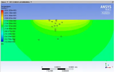
Adhesion Model: Simulation
Using ANSYS Fluent with a volume of fluid approach to track the molten aluminum-air
phase interaction, a single droplet falling under gravity and a defined inlet velocity is
simulated. Furthermore, temperature contours immediately after droplet impingement
are found. The contact angle is set at 180 degrees to ensure that the droplet does not
spread after contacting the surface and assumes a semi-spherical shape seen under laser
confocal microscope measurements of droplets impinging on a surface. Temperatures
are compared to the theoretical interfacial temperature models. Fig. 3.7 refers to the
simulation domain.
Figure 3.7: DROPLET IMPINGEMENT SIMULATION DOMAIN
Boundary Conditions
1. Velocity Inlet: 1m/s
2. Pressure Outlet: Ambient pressure at 0kPa
3. Surface Boundary: Coupled wall thermal condition
4. Droplet-Air Interaction: 0.5mW2K convection coefficient
Initital Conditions
1. Molten Al droplet at 950◦C
3. Air temperature assumed to be 15◦C
4. Volume fraction of molten droplet set to 1
5. Initial velocity of droplet set at 1 m/s
Figures 3.8-3.10 below depict temperature contours in the moments after the droplet
impinges on the aluminum chip surface. Continued heat transfer is seen over time from
3.21 ms to 6.27 ms in the form of conduction between the droplet and top of the chip
surface as well as through the chip surface to reach a penetration depth. For this study,
we are concerned with the hottest surface temperature which is needed to bond the
droplet to the surface. Note that the hottest temperature is between 915-992K or
642-719◦C. This is important as it indicates the immediate interface will reach an interfacial
[image:45.596.115.514.345.604.2]temperature very close or above the melting point of the solid aluminum surface.
34
Figure 3.9: TEMPERATURE CONTOURS AT 4.065 ms AFTER IMPINGEMENT
[image:46.596.118.518.456.711.2]Results
Additive manufacturing allows geometries catered towards enhancing boiling
perfor-mance. An experimental approach is used for both optimizing the Vader System
param-eters to create the desired microsctructures, and in determining its boiling performance.
Furthermore, high speed imaging is used to determine the mechanism of enhancement
and provide insight into the boiling process. Particle Image Velocimetry (PIV) is
uti-lized to capture flow field during low heat fluxes in order to draw support for conclusions
reached from high speed imaging.
4.1
Uncertainty Analysis–Heat Flux
An uncertainty analysis for the heat flux was performed to determine the level of
sys-tematic and random error within this study. All temperature readings are sampled at
10 Hz for a total of 10 seconds. This attempts to remove random error seen in the data
as well as average the data should steady state not be reached. The systematic error is
quantified below in Table 4.1.
From combining Fourier’s Law with the truncated Fourier series approximation for a
derivative we obtain:
Q”=−kAl
3T1−4T2+T3
2∆x
(4.1)
36
Table 4.1: SYSTEMATIC UNCERTAINTY
Variable Uncertainty Source
Thermal Conductivity (k) 0 mkW Assumed no variation with temperature
T1 0.1 K Thermocouple error
T2 0.1 K Thermocouple error
T3 0.1 K Thermocouple error
∆x 127∗10−6 Machining and grinding error
The uncertainty in each variable is determined and the total calculated uncertainty given
as the square root of the sum of the square of each uncertainty. Where ∆U refers to the
measured uncertainty in quantity U, ai refers to the measured variable, and ∆ai refers
to the uncertainty of the measured variable.
∆U =
v u u t N X i=1 ∂U ∂ai
∗∆ai
2
(4.2)
Using this equation with Equation 4.1we obtain the uncertainty in the heat flux.
∆Q”=
s
∂Q”
∂kAl
∗∆kAl
2 +
∂Q”
∂T1
∗∆T1
2 +
∂Q”
∂T2
∗∆T2
2 +
∂Q”
∂T3
∗∆T3
2 +
∂Q”
∂(∆x) ∗∆(∆x 2 (4.3)
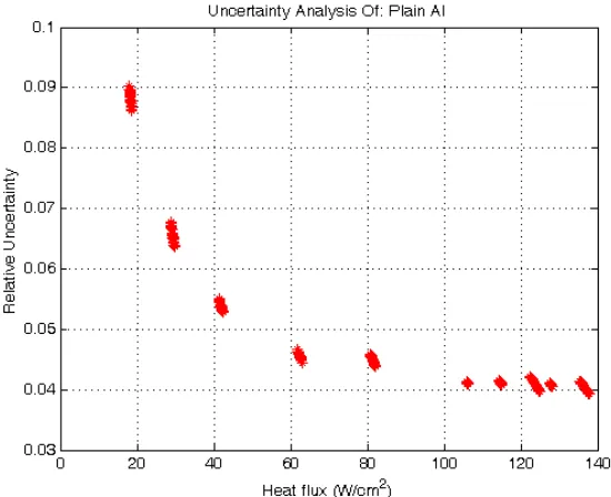
The uncertainty analysis for a plain aluminum chip is shown in Fig. 4.1. Note that as
the heat flux increases, the uncertainty decreases in an exponential decay fashion. All
heat flux measurements after 30W/cm2 are below 5% uncertainty.
4.2
Vader System - Process Parameters
After proving adhesion and locating on the chips, it was necessary to determine the
proper process parameters for consistent printing.
Regarding STL slicing parameters:
1. Using the pre-defined Slic3r software allows quick export to the Vader Gcode
Figure 4.1: UNCERTAINTY ANALYSIS FOR A PLAIN Al CHIP
resolve the thin structure contours (Fig. 4.2-4.3). To solve this problem, the nozzle
diameter in the software is reduced from 0.78 mm to 0.10 mm. Additionally a layer
height of 0.100 mm is used for all Slic3r prints. Notice that making this change
allows the full number of layers to be sliced (seen visually as the number of layers
near the top of the volcano in 4.3 is greater than 4.2). Additionally, this change
increases the resolution of the print by removing excess curves and irregularities.
2. For the angled fins, a MATLAB code was written to create the Gcode. A droplet
by droplet approach is incorporated to build up this structure. Since the angled
fin array could be written as a repetition of a single unit, an iterative approach is
taken to create the Gcode files.
Regarding the Vader printing parameters:
1. A drop spacing approach was used with a droplet distance of 0.300 mm. Next,
to achieve repeatable results, a track area of 0.125 mm was used with a variable
calibration mass. The track area refers to the area of a cross-section of jetted
material. It was found that the track area approach is best for repeatability and
quality of print. By calibrating before each print, it is possible to achieve high
repeatability in chip structures. Specifically, this method achieved repeatability
38
Figure 4.2: Slic3r NOZZLE DIAMETER SET TO 0.78 mm
Figure 4.3: Slic3r NOZZLE DIAMETER SET TO 0.10 mm
2. A bed temperature of 450◦C was used according to numerical and theoretical
results for bed adhesion. However, the build platform became limited to 400◦C.
[image:50.596.145.487.352.595.2]4.3
Vader System - Manufactured Chips
Each chip is fabricated using the Vader System’s magnetojet printing capabilities. Four
main chip varieties were manufactured with increasing complexity. First, various
print-ing parameters, adhesion, and bubble dynamics were tested on an angled pillar chip.
Next, a miniaturized volcano design was envisioned to force vapor exit from a singular
point. Third, a singular volcano design was enhanced with liquid inlet holes at the
bottom of the volcano to establish macro-scale separate liquid-vapor pathways. Finally,
this design was miniaturized to place four volcano-with-holes on a single 10 mm x 10
mm chip. These chips are discussed in subsequent sections and CAD renderings of each
design are seen in Fig. 4.4.
(a) (b)
[image:51.596.147.490.313.576.2](c) (d)
Figure 4.4: VADER SYSTEM CHIP DESIGNS:(a)Angled Pillar;(b) Miniaturized Volcano Array; (c)Volcano-With-Holes; and,(d)Miniaturized Volcano-With-Holes.
4.4
Initial AM Chip Performance
4.4.1 Angled Fin
The first Vader System fabricated chip was an array of angled pillars on the 10 mm x 10
40
code to make the machine Gcode. By using a low pulse distance (i.e. lower distance
between consecutive droplets), the droplets solidified on top of each other at an angle.
Experimental measurements indicate an angle of 54.64◦, height of 3.67 mm, and diameter
of 1.120 mm.
Figure 4.5: ANGLED PILLAR SCHEMATIC
The goal in this design was to see the evaporation momentum force push the nucleating
bubble away from the bottom of the angled pillar. Additionally, this was the first test
of a Vader System printed chips; therefore, adhesion was tested as well. During the
test, the chip displayed strong adhesion with no pillar breaking under the boiling forces.
However, th
![Figure 1.3: DIRECT METAL LASER SINTERING MACHINE [2]](https://thumb-us.123doks.com/thumbv2/123dok_us/32049.2541/20.596.230.401.547.664/figure-direct-metal-laser-sintering-machine.webp)

![Figure 1.6: MAGNETOJET PRINTING SCHEMATIC [5]](https://thumb-us.123doks.com/thumbv2/123dok_us/32049.2541/23.596.120.504.272.552/figure-magnetojet-printing-schematic.webp)