Abstract— This paper takes a systematic view on the control and protection of medium power DC networks in an active distribution power system considering fault current limiting, system control and converter design. Reduced terminal capacitance and extra DC impedance are used to limit DC fault current and reduce the required converter current rating for medium power DC networks. An adaptive DC power stabilizer is proposed to alleviate possible system instability brought by the fault current limiting settings in the presence of constant power load. The effect of the current limiting method and the proposed stabilizer on DC fault current and stability enhancement are validated by simulation studies using a simple two-converter DC network and a multi-terminal DC network in an active distribution power system.
Index Terms—DC power system, DC protection, DC stabilizer, active distribution power system, DC microgrid
I. INTRODUCTION
C power system has again become an attractive option in power transmission and distribution due to increasing power converter penetrations in modern power systems [1]. Modern power electronics converter based DC power systems can help traditional AC power systems to cope with arising renewable power generation and Electric Vehicle (EV) issues with more flexible controllability [2]. A DC power system can also benefit from simpler control compared to AC networks with no concern on frequency and reactive power. Furthermore, DC links transmit power with no need for synchronizing the inter-connected AC sides [3]. Such features make DC power system a promising solution to connect large AC power grids and reconfigure medium voltage distribution power systems [4].
As to the power distribution system, DC systems also simplify the integration of the mainstream renewable generations, photovoltaic and wind turbines for instance, as such generations all contain DC links. If these DC links are connected together along with storages and DC loads, a DC microgrid is formed [5-8]. A common DC/AC converter in such systems can save one-off cost and possibly give rise to
This work was supported in part by the UK Engineering and Physical Sciences Research Council: Grant EP/K03619X/1.
D. Chen is currently with Department of Engineering, Glasgow Caledonian University (email: Dong.Chen@gcu.ac.uk). L. Xu is with Department of Electronic and Electrical Engineering, University of Strathclyde, Glasgow, G1 1XW UK (email: lie.xu@strath.ac.uk). J. Yu is with SP Energy Networks, Blantyre, G72 0HT. (James.Yu@scottishpower.com).
lower conversion loss if most energy are consumed and stored on the DC side [6]. The concept of the DC microgrid can be extended to medium power distribution system with multiple DC/AC connections to form a future active distribution power system [9]. For example, the proposed DC network can be expanded up to a few kilometers between weak AC feeders. This allows a distribution system to gain additional AC voltage control ability and redistribute its instant power flow in a continuous and more optimal way [4] than a hard switch based active distribution power system [10] without increasing AC fault current. Such configuration further benefits from its compatibility with EV charging station.
protection [11][12], and in particular the effective protection of the converters after a DC fault due to the discharging of the DC link capacitors and fault current feeding from AC side via the freewheeling diodes in DC/AC converters is one of the major concern of modern DC power system. Fast acting DC Circuit Breakers (DCCBs), e.g. semiconductor based [13] can effectively isolate the fault within a short period (typically less than 1 ms) though with increased cost and conduction power loss. On the other hand, mechanical AC and DC Circuit Breakers [14] have negligible losses and lower cost but are with slow breaking response, typically over a few tens of mini-seconds. Fault Current Limiting (FCL) techniques are proposed to reduce the peak fault current and its rising rate to facilitate circuit breaking. Series impedance injection is the basic idea considered in DC fault current limiting. It can be divided into two main types: resistive and inductive. Superconductor based techniques are employed in resistive type FCL, but they consume considerable power during steady state operation in order to maintain superconductivity [15][16]. The other type is inductive based FCL [17] which can effectively limit fault current rising rate and reduce peak fault current though it does not reduce (or might even increase in some cases) the total discharging energy during a DC fault. If the DC current and fault energy can be limited to allow the converter to survive the fault transient before current interruption, AC side breakers or slow mechanical DCCBs can provide a much simpler and cost effective solution compared to the fast DCCB option.
Constant power loads (CPL) can potentially introduce system instability in a DC power system. The stabilization of CPLs in a small scale DC network within a confined area has
Adaptive DC Stabilizer with Reduced DC Fault
Current for Active Distribution Power System
Application
Dong Chen, and Lie Xu,
Senior Member, IEEE
and James Yu
This paper is a post-print of a paper submitted to and accepted for publication in IEEE Transaction on Power Systems and is subject to Institution of
Electrical and Electronic Engineering Copyright. The copy of record is available at IEEE Xplore Digital Library. 2 been well studied [18-29]. Adding physical resistors were
initially suggested though with considerable power losses [18]. Active damping was proposed thereafter [19-29]. Impedance matching based techniques were developed to modify the small signal characteristics at the point of load from the source side control [19-22], though with a fixed power flow direction. Global system stabilization was proposed based on state-space modeling to provide damping for bidirectional power flow [23-25]. However, both of the above two stabilization methods require real-time knowledge of the overall system configuration. This requires high bandwidth communication, which is neither economical nor reliable in a DC system with a considerable distribution length. In addition, the system configuration is not likely to be fixed in a broader network, where intermittent renewable sources, plug-and-play loads and system reconfigurations are expected. Local stabilization techniques are also proposed to be implemented on the load side [26-28] or constant power generation side [29]. The main drawback of these techniques is that they require the access to the control of the target converter terminals including their instant power, which makes these methods not applicable to systems with inaccessible constant power terminals. In addition, the rigid configurations of stabilizing algorithms make them sensitive to the variations of constant power terminals and system configurations.
The measure taken for fault current limiting using increased DC inductance and reduced DC capacitance can further tense up the instability problem along with considerable distribution length, which has rarely been investigated before. And the stabilization of a more expanded DC system, typically up to a few kilometers, with autonomous variable load has rarely been explored with DC protection simultaneously considered. In this paper, a systematic view on protection, stability control and converter design is taken to enable the application of medium power DC system with considerable distribution length. An adaptive stabilizer is proposed to compensate local negative impedance based on its own local detections hence no need for high bandwidth global information acquisition. The proposed adaptive control is also independent from both the constant power terminal and the grid side conditions, and the flexibility of being able to incorporate into CPL terminal control if required.
The paper is organized as followings. Section II briefly introduces the concept of medium power DC system for active distribution network and Section III analyzes DC fault behavior with various DC terminal impedances. Section IV presents the principles of the proposed integrated DC system with both DC fault current limiting and adaptive stabilization capabilities. Time domain case studies are performed in Section V and VI with a single power terminal and a three-terminal DC network embedded into an active distribution power system, respectively. The conclusion is finally drawn in Section VII.
II. INTRODUCTION TO ACTIVE DISTRIBUTION POWER SYSTEM
WITH MVDCNETWORK
With the increasing penetration of renewable generation on
the distribution power system, the growing intermittent power could potentially give rise to over-voltage or under-voltage at the “last-mile” feeders of a distribution power system. Medium power DC links can therefore be placed in between these weak feeders to improve their voltage profile and provide more flexible power flow regulations as is shown in Fig 1. As the possible increasing load demand of EV charging may arouse further load mismatching, one option is to integrate the charging station (and other renewable generations) on the DC link side as shown in Fig. 1. In this way the charging load flow and intermittent renewable power can be managed in a more flexible way. Such a system could further benefit from emergency power supply from the charging station along with renewable sources when there is an outage on the AC utility grid side.
Feeder 1 Feeder 2 ChargingStation
VSC VSC
Fig. 1. DC network in an active distribution power system
For a multi-terminal DC network within an active distribution power system, the AC/DC converters may be located some distance away from the loads including CPL (e.g. charging station) and for economical reasons existing overhead line paths may be used for DC distribution. As a result, possible DC fault has to be considered. Protecting the converters from DC faults and, meanwhile, ensuring DC system stability when there is considerable distance between the loads and AC/DC converters have to be dealt with.
III. DCFAULT AND FAULT CURRENT LIMITING
For medium power DC and distribution network applications, two-level VSCs are commonly used. In this section, typical DC fault behavior for two-level VSC based medium power DC power systems is analyzed.
A. DC fault of two-level VSC
In a two-level VSC based DC power system, the most critical fault is DC pole-to-pole short, as is shown by Fig. 2 where C1 refers to the terminal capacitance, Lac is the AC
reactance, R1 and L1 are the terminal impedance at the DC side, Vdc is the terminal DC voltage, and iLdc is the current flowing
through the DC impedance.
[image:2.612.320.544.235.302.2]Transformer Utility Grid L1
R1
C1 Vdc
+
-iLDC
Lac
① ②
③
Fig. 2. DC Fault at two-level VSC terminal
At stage ①, assuming all switching devices have been blocked, the fault circuit can be modeled as a serial RLC circuit. Assuming the resistance is relatively small for the worst case, the fault current is under-damped and its response in time domain can be estimated by [31]
( ) tsin
LDC peak r
i t I e t (1)
where Ipeak is the peak fault current, and α, ωr and φ are the
damping coefficient, resonance frequency and initial angle respectively. Assuming the energy dissipation on the resistance is negligible at the first oscillation cycle, Ipeak can be
approximated considering the complete transfer of the stored capacitor energy to the DC inductor at the end of Stage ①as
2 2
1 dc0/ 2 1 peak/ 2
C V L I (2)
where Vdc0 is the initial capacitor voltage. Thus
1/ 1 0
peak dc
I C L V (3)
As most of the stored energy in large terminal capacitance has to go through the converter diode during the fault, it can be inferred from (2) that the reduction of terminal capacitance can effectively reduce energy flowing through the diodes during a DC fault. From (3), it can be inferred that a smaller terminal capacitance and larger fault inductance can both effectively reduce the peak fault current which will flow into the converter diodes in Stage ②. The rising time of the fault current Tr can be estimated by
1 1
2 / (4 ) / 4
r r
T L C (4)
and the average current rising rate diLDC/dt can be
approximated by
1
/ / / 4
LDC peak r dc
di dtI T V L (5)
From (5), it can be inferred that the inductance plays a main role in limiting the fault current rising rate.
B. Fault behavior simulation and parametric analysis
A parametric case study is carried out in this section to investigate the effect of various parameters on fault current. The initial parameters of the DC terminal are set as the following: rated power 2 MW, AC nominal frequency 50Hz, AC and DC nominal voltage 690V and 1200V respectively, equivalent AC inductance (including both AC reactance and transformer) 0.2 p.u., C1 20 mF with Equivalent Series
Resistance (ESR) and Equivalent Series Inductance (ESL) considered [32], R1 0.72 mΩ and L1 0.015 mH (equivalent
impedances of a 100-meter line).
The DC fault behavior is depicted in Fig. 3(a) where the DC fault occurs at t = 0 ms. No current limiting measure is taken and the IGBTs are assumed to be blocked immediately after the fault. As a result the DC voltage Vdc drops to 0 and
the fault current iLDC reaches as much as 42.27 kA (25.36 p.u.)
in less than 1 millisecond. This peak current is mainly produced by the discharging of the terminal capacitor. The discharging current in Stage ① and the subsequent circulating current in Stage ② are the main fault current components after the fault. The converter diodes have to withstand such an excessive transient current with a di/dt rate of 30 p.u./ms in the worst case.
By reducing the capacitance from 20 mF to 4 mF, the results are obtained in Fig. 3 (b). It can be seen that the peak current is significantly reduced to 19.1 kA (11.46 p.u.) though the maximum di/dt remains largely unchanged. This is due to the fact that a smaller terminal capacitance has reduced the total capacitor discharging energy at Stage ① shown in Fig. 2. The fault current decays and circulates through the diodes after the DC voltage reaches 0. The infeed current from AC side becomes the main component after T = 7 ms when the most of discharging energy has dissipated.
T/ms
VD
C
/k
V
ILD
C
/k
A
-0.5 0 0.5 1.0 1.5
0 3 6 9 12 15
0 10 20 30 40 50
(a) 20 mF DC capacitance without extra DC inductance
-0.5 0 0.5 1.0 1.5
0 3 6 9 12 15
0 10 20 30 40 50
T/ms
VDC
/k
V
ILD
C
/k
A
(b) 4 mF DC capacitance without extra DC inductance
T/ms
VDC
/k
V
ILD
C
/k
A
-0.5 0 0.5 1.0 1.5
0 3 6 9 12 15
0 10 20 30 40 50
[image:3.612.49.283.52.144.2] [image:3.612.326.544.325.712.2]This paper is a post-print of a paper submitted to and accepted for publication in IEEE Transaction on Power Systems and is subject to Institution of
Electrical and Electronic Engineering Copyright. The copy of record is available at IEEE Xplore Digital Library. 4 Based on the case shown in Fig. 3 (b), an extra terminal
impedance of 7.2 mΩ / 0.15 mH is added to the equivalent DC
resistance and inductance R1 and L1 to total values of 7.92 mΩ
and 0.165 mH, respectively. The fault behavior with reduced capacitance and extra DC impedance is given in Fig. 3 (c). The extra inductance further reduces the fault current rising rate during stage ① and the peak discharging current has been suppressed to less than 4 p.u. when the DC voltage drops to 0. After t = 4 ms, the AC infeed current becomes the main fault current component and due to the existence of the AC side inductance it is a much slower process. The fault current reaches its peak point at 10 ms with a peak value of 10.66 kA
(6.4 p.u.) and the maximum di/dt rate is reduced to 2.68
p.u./ms. As can be seen, the capacitor discharging current is no longer the main component of the fault transient leading to reduced fault current flowing through the diode and their thermal rating requirement.
TABLEISUMMARY OF DC FAULT SCENARIOS
Scenario C1 (mF)
L1(mH) R1(mΩ) Ipeak(pu) di/dt
(pu/ms)
I Fig. 2(a) 20 0.015 0.72 25.36 30.00
II Fig. 2(b) 4 0.015 0.72 11.46 29.92
III Fig. 2(c) 4 0.015 +0.15 0.72+7.2 6.4 2.68
The DC fault case scenarios are summarized in Table I. It shows that reducing DC capacitance and increasing DC inductance at the same time can significantly reduce both the fault current and its di/dt.
IV. PRINCIPLES OF THE ADAPTIVE DCPOWER STABILIZER
As previous described, a reduced DC capacitances with extra impedance on the DC terminal can effectively reduce the DC fault current. However, such arrangements can potentially cause system instability especially when connecting to a remote constant power terminal [23]. To tackle this problem, an adaptive DC power stabilizer is proposed for stabilizing the DC power system with small DC capacitance and additional DC terminal impedance.
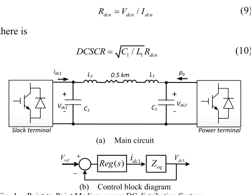
In this section, the dynamic effect brought by the extra impedance for DC fault current limiting is analyzed first to show how the FCL configuration can deteriorate system stability when there is CPL in operation. Based on the analysis, an adaptive DC power stabilizer is then proposed and installed at the CPL terminal to avoid potential system instability. Given a point-to-point DC system as shown in Fig. 4 (a), the dynamics of a single constant power terminal is analyzed in frequency domain for dynamic and stability assessment.
Defining the DC short circuit peak current Ipeak for Stage
① as
peak dcn
I
DCSCR I
(6)where DCSCR is the DC short circuit ratio and Idcn is the
nominal DC current for the converter, which is defined by
/
dcn n dcn
I
P V
(7)Substituting (6) and (7) into (3) yields
1/ 1 dc0/ dcn
DCSCR C L V I (8)
Assuming Vdc0 = Vdcn and defining the equivalent nominal
resistance Rdcn as
/
dcn dcn dcn
R V I (9)
there is
1/ 1 dcn
DCSCR C L R (10)
C1 C1
Vdc1
Power terminal
+
-+
-pp 0.5 km
L1 L1
Vdc2
Slack terminal idc1
(a) Main circuit
eq Z ( ) Reg s
ref
V Vdc1
1 dc i
(b) Control block diagram Fig. 4. Point-to-Point Medium power DC distribution System
In a DC power system, larger constant power terminal tends to cause oscillation when there are large DC impedance and small capacitances due to the induced equivalent negative admittance [20]. Assuming the constant power flowing out from the DC network is Pp, there is
p dcp dcp
P V I (11)
where Vdcp is the local DC voltage of the constant power
terminal and Idcp is the equivalent DC current. The equivalent
small signal resistance Rp can be given by 2
1/Rp P Vp/ dcp (12)
Figs. 4 (a) and (b) show the simplified diagrams of a point-to-point Medium DC power distribution system and its control, respectively. As shown in Fig. 4 (b), Reg(s) is the slack terminal controller which regulates the DC voltage, and
Zeq(s) is the equivalent virtual impedance from the slack
terminal side [33]. Reg(s) can be expressed as the following [33]:
1
( )
( )
(1 )
p i
s k s k C Reg s
T s s
(13) where kp and ki are the proportional and integral gains of the
DC voltage PI controller, and Ts is the current loop delay time
constant. The equivalent virtual impedance Zeq(s) can be
expressed as [32]
( ) ( ) / ( )
eq
Z s N s D s (14)
3 2
2 2 2
2
( ) ( )
( )
p p p p p
p p p p
N s R LC T s RR C T R LC s
R T RR C L s R R
4 3
1 2 1 2 1 2 1
2
1 2 1 2 1 1 2
( ) ( ) (
) ( ) 1
p p p p p p p
p p p p l
D s R LC C T s RR C C T R LC C s R C T
RR C C LC R C T s R C RC R C s
[image:4.612.314.563.98.292.2]This paper is a post-print of a paper submitted to and accepted for publication in IEEE Transaction on Power Systems and is subject to Institution of
Electrical and Electronic Engineering Copyright. The copy of record is available at IEEE Xplore Digital Library. 5 power loop delay time constant.
A root locus can be drawn with variable DCSCR (varying DC side capacitance and inductance values) as Fig. 5 (a) shows based on the transfer function of
1
( ) ( )
1 ( ) ( )
ref eq
dc eq
V Reg s Z s
V Reg s Z s (15)
Based on Fig. 4, it is assumed that both terminals are 2MW system with nominal DC voltage at 1200V, line impedance at 0.15 mH/km and 7.2 mΩ/km, Ts at 0.2 ms, Tp at 0.8 ms, initial
terminal capacitances C1 and C2 both at 20 mF, initial terminal
impedance equivalent to 0.05 km line inductance. Since reducing terminal capacitance and inductance will both contribute to lower value of DCSCR, the variable capacitances
C1’, C2’ and L1’ are assumed to vary at the same ratio (for
simplicity) against the initial values C1, C2 and L1 respectively
as
1'/ 1 2'/ 2 1/ 1' / '
C C C C L L DCSCR DCSCR k (16)
It can be seen in Fig. 5 (a) that the system tends to be unstable when k is changing from 1 to 10 when the DCSCR’ is reduced correspondingly.
To deal with the problem caused by the extra impedance, a passive resistance in parallel with the constant power terminal is added to cancel the negative terminal admittance introduced by the constant power terminal. Adding a 1.025 MW (at nominal voltage) resistive load at the power terminal side can modify its root locus as Fig. 5 (b) shows. It can be seen that the system is stable across a large variation of DCSCR. However, the consequent power loss is excessive and such a scheme is obviously not practical. An alternative implementation is therefore proposed to employ a converter that is able to mimic the small signal behavior of a passive resistance without resistive power consumption.
To fully cancel out the negative resistance, there are
1/Rv 1/Rp (17)
2
1/RvP Vp/ dcp (18)
1/Rv1/Rp1/Rv' (19)
where Rv is the added virtual resistance and Rv’ is the net
resistance after compensating the negative resistance Rp that
can provide extra positive damping for the DC terminal. The system configuration is demonstrated in Fig. 6 (a) where a shunt DC stabilizer is placed at the constant power terminal to actively mimic the passive resistance. The equivalent virtual impedance is shown in Fig. 6 (b). It is possible to incorporate the stabilization control into the conventional active current control of the CPL terminals if their control systems can be accessed. As is illustrated in Fig. 6 (c), the stabilizer DC current idcs is converted to the d-axis component ids using the
d-axis voltage Ud and is added to the active current reference
when d-axis voltage oriented control is employed for the CPL.
Real Axis (seconds-1)
Im
ag
in
ar
y
A
xi
s
(s
ec
on
ds
-1)
-60 -40 -20 0 20 40 60 80 -60
-40 -20 0 20 40 60
From: Single
CPLtrsfunc/In1 To: Virtual Impedance
k=10
DCSCR 10 tims lower
k=1
DCSCR high
Real Axis (Seconds-1)
Im
ag
in
ar
y
A
xi
s
(S
ec
on
ds
-1)
(a) Without DC stabilizer
Pole-Zero Map
Real Axis (seconds-1)
Im
ag
in
ar
y
A
xi
s
(s
ec
on
ds
-1)
-34 -33.5 -33 -32.5 -32 -31.5 -31 -40
-20 0 20 40 60
k=1
DCSCR high DCSCR 10 tims lowerk=10
Real Axis (Seconds-1)
Im
ag
in
ar
y
A
xi
s
(S
ec
on
ds
-1)
(b) With resistive DC stabilizer Fig. 5. Root Locus with variable DCSCR
Cp
Constant Power Terminal DC Stabilizer
IdcT IdcP IdcS
IdcC
(a) Physical DC Stabilizer configuration
Cp
Rp
-Rp
Stabilizer CPT
Rv’
Idct
Idcc
Idcp
(b) Equivalent virtual impedance
dref i
d i
Current regulation
From active power control
From active power control
dcs
i 2
3
d
dc
U V
From DC Stabilizing control
From DC Stabilizing control
dref V
ds i
(c) Virtual DC stabilizer control Fig. 6. DC stabilizer
As can be inferred from (12), the power terminal induces the largest negative incremental admittance when consuming the maximum power. Therefore, the virtual resistance is configured to compensate the negative admittance corresponding to the maximum power as
2 max
/
p dc
R V P (20)
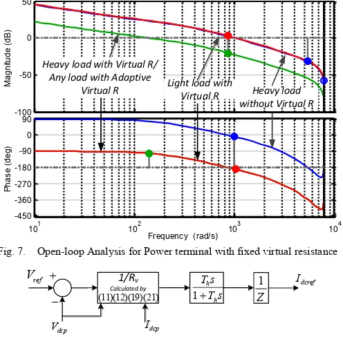
By setting the terminal capacitance at 2 mF, constant power terminal rating at 4 MW and rated DC voltage at 1200 V, an open-loop analysis is performed with variable terminal power and the results are shown in Fig. 7 for illustration. It can be seen that a positive equivalent system resistance can be guaranteed at the maximum constant terminal power Pmax if
[image:5.612.312.536.52.552.2]This paper is a post-print of a paper submitted to and accepted for publication in IEEE Transaction on Power Systems and is subject to Institution of
Electrical and Electronic Engineering Copyright. The copy of record is available at IEEE Xplore Digital Library. 6 However, such a fixed virtual resistance designed for
maximum load can result in too large open-loop gain and can induce oscillations due to its poor or even negative gain margin during light load condition, as is illustrated in Fig. 7.
In order to deal with the problem caused by the use of fixed virtual resistance, an adaptive virtual resistance is proposed. The instant negative resistance brought by the CPL can be estimated by considering
/
p dcP dcT
R V I (21)
where IdcT is the actual DC current flowing to the CPL
terminal.
By using the adaptive Rp calculated using (21) rather than
(20) the open loop behavior of the CPL terminal is independent of loading condition and traces a predefined response with sufficient margins, as shown in Fig. 7. Therefore, only local current and voltage detections are needed for the proposed stabilizer hence it is not sensitive to either the CPL variation or the grid side characteristics at the point of integration.
Frequency (rad/s)
101 102 103 104
-450 -360 -270 -180 -90 0 90
P
ha
se
(
de
g)
-100 -50 0 50
M
ag
ni
tu
de
(
dB
)
Heavy load without Virtual R Heavy load with Virtual R/
Any load with Adaptive
Virtual R Light load with Virtual R
Fig. 7. Open-loop Analysis for Power terminal with fixed virtual resistance
ref
V
(11)(12)(19)(21) 1
h
h T s T s
Z1
dcp
V Idcp
dcref I 1/Rv
Calculated by
Fig. 8. Adaptive Control of DC Stabilizer
Based on (19) and Fig. 6 (b), the control diagram of the proposed adaptive conditioner can be shown by Fig. 8, where a first-order high-pass filter with a large time constant is added to ensure a zero average current during steady state. In Fig. 8, the digital control and current loop delay is modeled as a first-order delay whose time constant can be equal to or larger than the switching cycle of the converter depending on control implementation.
V. CASE STUDY OF DCPOWER CONDITIONER
In this section medium power DC power systems are established to test the dynamic behavior of the proposed DC stabilizer with extra fault current limiting behavior.
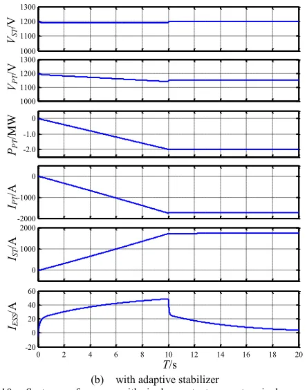
A single constant power terminal based DC power network
is established as shown in Fig. 9. Two-level VSCs and additional DC impedances for extra fault limiting capability are employed to integrate the DC system to the AC utility grid. One VSC operates as the constant power terminal and the other is the slack terminal controlling the DC voltage. The distance between the two converters is 2 km. A small DC-DC converter with supercapacitor based energy storage system (ESS) is placed at the constant power terminal side as the power stabilizer. The constant power terminal current iPT,
slack terminal current iST and the power conditioner terminal iESS are defined along with the DC voltage of the slack
terminal VST and power terminal with VPT accordingly. Both
fault current limiting inductors L1 and L2 are at 0.15 mH / 7.2
mΩ. The line impedance is set at 0.15 mH/km and 7.2 mΩ/km.
L1
L2
CST
C2 VPT VST
Feeder 1
+
-+
-iESS
iST
Feeder 2
iPT
Constant Power
Terminal Slack Terminal
Power Conditioner
2 km
Fig. 9. Sample system with single power terminal and conditioner
By deactivating the power stabilizer, the system is tested with a defined power ramp of 0.2 MW/s from the constant power terminal. The simulation results are shown in Fig. 10 (a). It can be seen that when the power terminal starts to drain power from the DC network, the current are balanced by the slack terminal accordingly. However, when the power reaches approximately 1.1 MW at T = 5.7 s, the system starts to oscillate since the remote slack terminal cannot accommodate the negative resistance produced by the constant power load.
0 2000 4000
0 2000 4000
-2.0 -1.0 0
-2000 -1000 0
0 1000 2000 3000
0 1 2 3 4 5 6 7
-20 0 20 40 60
T/s
VST
/V
VPT
/V
PPT
/M
W
IPT
/A
IST
/A
IESS
/A
[image:6.612.313.563.239.317.2] [image:6.612.50.298.298.542.2] [image:6.612.329.545.452.727.2]1000 1100 1200 1300
1000 1100 1200 1300
-2.0 -1.0 0
-2000 -1000 0
0 1000 2000
0 2 4 6 8 10 12 14 16 18 20
-20 0 20 40 60
T/s
VST
/V
VPT
/V
PPT
/M
W
IPT
/A
IST
/A
IESS
/A
[image:7.612.62.284.51.333.2](b) with adaptive stabilizer
Fig. 10. System performance with single constant power terminal
On the contrary shown in Fig. 10 (b), the DC stabilizer is activated and the power ramp of the constant power terminal starts from T = 0 s and ends at T = 10 s. The DC voltages are well regulated throughout. The power stabilizer only consumes 50 A at its peak, which is less than 3% of the rated current of the constant power terminal and gradually drops to zero after the ramp indicating only a small energy and power rating is required for the storage.
VI. APPLICATION OF MVDC NETWORK WITHIN AN ACTIVE
DISTRIBUTION NETWORK
To further examine the effectiveness of the DC current limiting capability and stability enhancement of the proposed system configuration and power stabilizer concept, a 7-feeder active distribution power system is established as Fig. 11 shows with its parameters listed in Table II. A three-terminal medium power DC network is inserted between Feeder 3 and Feeder 6 with an EV charging station incorporated.
VSC 6 (at Feeder 6) is designed to be the main constant power terminal within the DC power system whose internal control is typically accessible by the system operator for illustration. On the other hand, a charging station is incorporated in the DC system operating as an inaccessible/independent constant power terminal. VSC 3 operates as the slack terminal throughout the tests in this section.
A virtual DC stabilizer is incorporated within the accessible constant power terminal side (i.e. VSC 6) as shown by the dotted diagram in Fig. 11 and an actual DC stabilizer is installed at the inaccessible power terminal of the charging station in Fig. 11. All the DC terminals are designed with extra fault limit capability and the charging station is assumed to be
able to isolate the DC fault current with galvanic isolated topology.
Transmission Network
33 kV 33 kV
110 kV / SCR = 200 MVA
Feeder 1
Feeder 2
Feeder 3
Feeder 4
Feeder 5
Feeder 6 VSC 3 VSC 6
Charging Station
DC Stabilizer
Feeder 7
Fault 2
Fault 1
distribution line load switch circuit breaker
Stabilizing control
20MVA / 8 % 20MVA / 8%
21 km
24 km
1.5 km
17 km
[image:7.612.311.563.78.309.2]25 km
[image:7.612.316.546.330.509.2]Fig. 11. Active distribution power system configuration
TABLE II. DISTRIBUTION POWER SYSTEM PARAMETERS Nominal Voltage and Ratings
Distribution nominal voltage 33 kV Transmission nominal voltage 110 kV Transmission short circuit rating 200 kVA Transformer power rating 20 MVA Primary inductance 0.04 p.u. Secondary inductance 0.04 p.u.
AC distribution impedance 0.136 Ω/km, 0.356 mH/km and 0.262 nF/km [34] Feeder Load
Feeder 1: 0.15+j0.05 p.u.
Feeder 2: 0.5+j0.05 p.u.
Feeder 3 0.05+j0.01 p.u.
Feeder 4 -0.1+j0.01 p.u.
Feeder 5 -0.25+j0.01p.u.
Feeder 6 -0.05+j0.01 p.u.
Feeder 7 0.005+j0.001 p.u.
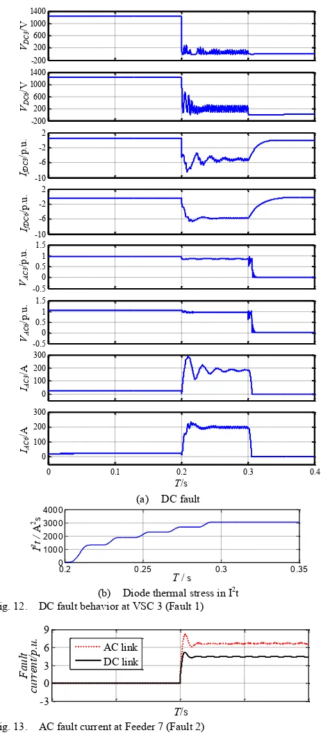
Fig. 12(a) shows the DC fault behavior at VSC 3 which connects to Feeder 3. The system starts with VSC 6 importing a ramp power of 0.25 MW/s to the DC network and the charging station is idle. When a DC fault occurs at 0.2 s, both DC voltages at VSC 3 and 6 quickly drop to almost 0 within 10 ms. Upon detection of the fault, both VSC 3 and 6 are blocked and the DC fault currents rise up to 8 p.u. at VSC 3 (IfDC3) and 6 p.u. at the VSC 6 (IfDC6). The corresponding AC
fault currents IAC3 and IAC7 rise up to about 300 A (8.57 p.u.)
and 210 A (6 p.u.) at VSC 3 and VSC 6 respectively. At 0.3 s, the circuit breakers at the AC sides of the VSC 3 and 6 are tripped to break the DC fault. As a result, the fault currents at both AC and DC sides are gradually extinguished and DC network is de-energized.
As the IGBTs of the converter are blocked after the fault, the VSC fault current all goes through the diodes. Diodes’ accumulated I2t during transient is a good indicator for
This paper is a post-print of a paper submitted to and accepted for publication in IEEE Transaction on Power Systems and is subject to Institution of
Electrical and Electronic Engineering Copyright. The copy of record is available at IEEE Xplore Digital Library. 8 which reaches 3.083 kA2s within 100 ms after the fault till
current interruption. By choosing the diodes with average current rating at 3000 A (1.8 p.u. based on nominal AC current), the maximum I2t allowance is 4.48 kA2s[35], which
is sufficient for the diodes in the VSC to withstand the over-current before fault interruption. Since modern commercially available DC circuit breaker can normally interrupt current in 40-60 ms [14], there is sufficient timing tolerance in this case.
VD C 3 /V VD C 6 /V
IfDC
3
/p
.u
.
IfDC
6
/p
.u
.
VAC
3
/p
.u
.
VAC
6
/p
.u
.
IAC
3
/A
IAC
6 /A T/s -200 200 600 1000 1400 -200 200 600 1000 1400 -10 -6 -2 2 -10 -6 -2 2 -0.5 0 0.5 1 1.5 -0.5 0 0.5 1 1.5 0 100 200 300
0 0.1 0.2 0.3 0.4
0 100 200 300
(a) DC fault
T / s
I
2t /
A
2s
0.2 0.25 0.3 0.35
0 1000 2000 3000 4000
[image:8.612.53.284.161.689.2](b) Diode thermal stress in I2t Fig. 12. DC fault behavior at VSC 3 (Fault 1)
-3 0 3 6 9
0 0.1 0.2 0.3 0.4
[image:8.612.317.564.356.490.2]-0.5 0 0.5 1 1.5 AC link DC link T/s F au lt cu rr en t/ p. u.
Fig. 13. AC fault current at Feeder 7 (Fault 2)
Fig. 13 shows the AC fault current comparison when an AC fault occurs at Feeder 7 (Fault 2 shown in Fig. 11). The system operates at steady state when a three phase short happens at Feeder 7 at 0.2 s. The fault current reaches about 5 p.u. and
then drops back to about 4.5 p.u. when there is a medium power DC network. On the contrary, when the DC link is replaced by a 2 km AC distribution line between Feeders 3 and 6, the AC fault current is increased to approximately 7.5 p.u. as shown in Fig. 13. This demonstrates the superiority of the DC link over the AC link, as it does not reduce the equivalent short circuit impedance whereas the additional AC connection does.
Figs. 14 (a) and (b) compare the performances with and without the stabilizer at the charging station under charging load ramp conditions. In Fig. 14 (a), both the stabilizing control in VSC 6 and the charging station are deactivated. A ramp load of 0.5MW/s is consumed at the charging station from T = 0 s till it reaches its full rating of 2 MW and the power is fully accommodated by VSC 3 as VSC 6 is given zero power order. It can be seen that when the charging power rise up to 1.9 MW, the DC system starts to oscillate. On the contrary, the ramp charging load test is performed in Fig. 14 (b) with charging side stabilizer activated. It can be seen that no oscillation is induced throughout this test. The maximum power shared by the stabilizer is less than 0.1 MW, which is 5% of the load rating. The stabilizing power gradually moves towards 0 from 4 s, since the stabilizer function only provides dynamic response due to the addition of the high-pass filter design shown in Fig. 8.
-2 0 2 -2 0 2 1.0 1.2 1.4
0 1 2 3 4 5
-0.1 0 0.1 VD C / k V P co n d / M W P ch ar g / M V
PDC
6
/ M
V
T/s
VDC / k V P co n d / M W P ch ar g / M V
PDC
6 / M V T/s -2 0 2 -2 0 2 1.0 1.2 1.4
0 1 2 3 4 5
-0.1 0 0.1
(a) without any stabilizer (b) with charging stabilizer Fig. 14. Single stabilizer performance at the charging station with ramp charging load; PDC3: power consumed by VSC 3, PCharg: power discharged from the charging station, VDC: DC voltage at the charging station bus, PCond: power discharged by the DC stabilizer.
VDC / k V P co n d / M W P ch ar g / M V
PDC
6 / M V T/s -2 0 2 -2 0 2 1.0 1.2 1.4
0 1 2 3 4 5
-0.01 0 0.01 -2 0 2 -2 0 2 1.0 1.2 1.4
0 1 2 3 4 5
-0.020 0.02
VDC / k V P co n d / M W P ch ar g / M V
PDC
6
/ M
V
T/s
(a) with only charging stabilizer (b) with both stabilizers Fig. 15. Dual stabilizer performance with power ramp at VSC 6, PDC6: power consumed by VSC 6, PCharg: power discharged from the charging station, VDC: DC voltage at the charging station bus, PCond: power discharged by the stabilizer.
[image:8.612.316.563.534.663.2]VSC 6 stabilizing control (virtual stabilizer) during power ramp of VSC 6 from 0 to 2 MW at 0.5 MW/s starting from 0 s. As shown in Fig. 15 (a) significant voltage oscillation is induced when the VSC 6 load increases to approximately 1.9 MW. However, when the stabilizing control is activated the oscillation is eliminated and system is completely stable across the whole power range, as can be seen in Fig. 15 (b). The maximum power of the actual stabilizer is only 0.01 MW (when system stable) indicating that the remote power terminal and its additional stabilizing control has negligible effect on the stabilizer at the charging station side. This result shows that the proposed stabilizer is not sensitive to remote variations.
The results shown in Figs. 14 and 15 clearly show that the proposed stabilizers can effectively eliminate undesirable oscillations caused by additional DC side impedance and constant power load in medium power DC network of an active distribution power system. In order to effectively stabilize the DC power system, real and/or virtual stabilizers need to be located close to the constant power loads. It can also be seen that the stabilizer (either physical or virtual) can effectively neutralize instability effect though; it has very little effect on the remote constant power terminal and vice versa.
The required power rating of the stabilizer is very small compared to the power rating of the system and thus the additional cost of the stabilizer is trivial compared to the overall system cost. In addition, this allows the adoption of simple fault current limiting method using additional DC inductance and reduced DC capacitance. As the fault current and discharged energy are significantly reduced, this can lead to reduced converter size (diodes) and simple protection arrangement.
VII. CONCLUSION
In this paper, a medium power DC system solution considering DC fault current limiting and stability for active distribution power system has been investigated. By replacing the normal open switch with a DC link, the distribution network achieves improved power distribution control and loadability without increasing AC fault current.
Increasing DC inductance and reducing DC capacitance of the DC terminals can effectively reduce VSCs’ peak fault current, current rising rate and accumulated diode I2t before
fault current interruption. However, this technique can give rise to instability when there are large CPL terminals within the medium power DC system due to the amplification of CPL’s negative impact on small-signal stability by the additional DC inductance and reduced DC capacitance. To overcome the adverse effect on stability and alleviate sensitivity to system operational conditions, an adaptive DC stabilizer with limited power rating requirement is proposed which can either be placed close to the inaccessible CPL terminal or with its control function embedded into an accessible CPL control as a virtual stabilizer. The proposed DC stabilization scheme requires only local measurements and enables the use of simple fault current limiting methods by effectively stabilizing a DC system of considerable
distribution length. The stabilizing control has been validated by simulations of a two-terminal DC system and a multi-terminal DC system in an active distribution network.
REFERENCES
[1] K. Kurohane, T. Senjyu, A. Uehara, A. Yona, T. Funabashi and Chul-Hwan Kim, "A hybrid smart AC/DC power system," in Proc. 2010 the 5th IEEE Conference on Industrial Electronics and Applications
(ICIEA), pp.764-769, 15-17 June 2010
[2] P. Goli and W. Shireen, "PV integrated smart charging of PHEVs based on DC link voltage sensing," IEEE Trans. Smart Grid, vol. 5, no. 3, pp.1421 -1428, 2014
[3] J. Yu, M. Xiao and G. G. Karady, "Dynamic Performance of Embedded HVDC with Frequency Control Strategy," in Proc.2015 the Power and
Energy Society General Meeting (PESGM), 2015
[4] J. Alcala,; V. Cardenas, J. Perez-Ramirez,; R.J. Betancourt, H. Miranda, "Improving power flow in transformers using a BTB converter to balance low voltage feeders," in Proc. 2012 IEEEEnergy Conversion
Congress and Exposition (ECCE), pp.2038-2044, 15-20 Sept. 2012
[5] H. Kakigano, Y. Miura and T. Ise, "Low-voltage bipolar-type dc microgrid for super high quality distribution", IEEE Trans. Power
Electron., vol. 25, no. 12, pp.3066 -3075, 2010
[6] D. Salomonsson, L. Soder and A. Sannino, "An adaptive control system for a dc microgrid for data centers", IEEE Trans. Ind. Appl., vol. 44, no. 6, pp.1910 -1917, 2008
[7] D. Chen and L. Xu, "Autonomous dc voltage control of a dc microgrid with multiple slack terminals", IEEE Trans. Power Syst., vol. 27, no. 4, pp.1897 -1905, 2012
[8] X. Lu, J. Guerrero, K. Sun and J. Vasquez "An improved droop control method for dc microgrids based on low bandwidth communication with dc bus voltage restoration and enhanced current sharing accuracy", IEEE
Trans. Power Electron., vol. 29, no. 4, pp.1800 -1812, 2014
[9] M. Barragan, J.M. Mauricio, A. Marano, M. Nieves, J. Churio, J.M. Maza-Ortega, E. Romero and A. Gomez, "Operational benefits of multiterminal DC-links in active distribution networks," in Proc.2012
IEEE Power and Energy Society General Meeting, 22-26 July 2012
[10] M. E. Baran and F. F. Wu, "Network reconfiguration in distribution system for loss reduction and load balancing", IEEE Trans. Power Del., vol. 4, no. 2, pp.1401 -1407, 1989
[11] D. Salomonsson, L. Soder and A. Sannino, "Protection of low-voltage DC microgrids", IEEE Trans. Power Del., vol. 24, no. 3, pp.1045 -1053, 2009
[12] S. D. A. Fletcher , P. J. Norman , S. J. Galloway , P. Crolla and G. M. Burt "Optimizing the roles of unit and non-unit protection methods within dc microgrids", IEEE Trans. Smart Grid, vol. 3, no. 4, pp.2079 -2087, 2012
[13] K. Sano and M. Takasaki "A surgeless solid-state DC circuit breaker for voltage-source-converter-based HVDC systems", IEEE Trans. Ind. Appl., vol. 50, no. 4, pp.2690 -2699, 2013
[14] EATON: PVGard 600 and 1000 Vdc solar photovoltaic circuit breakers [Online]. Available:
http://www.eaton.com/Eaton/ProductsServices/Electrical/ProductsandSe rvices/CircuitProtection/MoldedCaseCircuitBreakers/DCBreakers/
[15] M. Noe and M. Steurer, “High-temperature superconductor fault current limiters: Concepts, applications, and development status,” Supercond.
Sci. Technol, vol. 20, pp. R15–R29, Mar. 2007.
[16] C. Schacherer, J. Langston, M. Steurer, and M. Noe, “Power hardware- in-the-loop testing of a YBCO coated conductor fault current limiting module,” IEEE Trans. Appl. Supercond., vol. 19, no. 3, pp.1801–1805, Jun. 2009.
[17] C,M. Frank, “HVDC Circuit Breaker: A Review Identify Future Research Needs,” IEEE Trans. Power Del., vol. 26, no. 2, pp. 998–1007, Dec. 2007.
[18] M. Cespedes, L. Xing, and J. Sun, “Constant-power load system stabilization by passive damping,” IEEE Trans. Smart Grid, vol. 26, no. 7, pp. 1832-1836, Jul. 2011.
[19] W. Du, J. Zhang, Y. Zhang and Z. Qian, “Stablity Criterion for Cascaded System With Constant Power Load,” IEEE Trans. Power
Electron., vol. 28, no. 4, pp. 1843–1851, Apr. 2013.
This paper is a post-print of a paper submitted to and accepted for publication in IEEE Transaction on Power Systems and is subject to Institution of
Electrical and Electronic Engineering Copyright. The copy of record is available at IEEE Xplore Digital Library. 10
[21] X. Feng, J. Liu, and F.C. Lee, “Impedance Specifications for Stable DC Distributed Power Systems,” IEEE Trans. Power. Electron., vol. 17, no. 2, pp. 157–162, Mar. 2002.
[22] A. Emadi, A. Khaligh, C. H. Rivetta and G. A. Williamson, “Constant Power Loads and Negative Impedance Instability in Autonomous Systems: Definition , Modeling, Stability and Control of Power Electronic Converters and Motor Drives,” IEEE Trans. Vechinology
Technology, vol. 55, no. 4, pp. 1112–1125, Jul. 2006.
[23] A.A.A. Radwan and Y.-R. Mohamed "Linear active stabilization of converter-dominated dc microgrids", IEEE Trans. Smart Grid, vol. 3, no. 1, pp.203 -216, 2012
[24] P. Magne ,B. Nahid-Mobarakeh and S. Pierfederci "General active global stabilization of multi-loads DC-power networks", IEEE Trans.
Power Electron., vol. 27, no. 4, pp.1788 -1798, 2012
[25] P. Magne ,B. Nahid-Mobarakeh and S. Pierfederci "Dynamic Consideration of DC Microgrids With Constant Power Loads and Active Damping System-A Desgin Method for Fault-Tolerant Stabilizing System," IEEE Jounrnal of Emerging and Selected Topics In Power
Electronics, vol. 2, no. 3, pp.562 - 57, Sept. 2014
[26] Y. A.-R. I. Mohamed, A. A. A. Radwan, and T. K. Lee, “Decoupled reference-voltage-based active dc-link stabilization for PMSM drives with tight-speed regulation,” IEEE Trans. Ind. Electron., vol. 59, no. 12, pp. 4523–4536, Dec. 2012.
[27] W.-J. Lee, and S.-K. Sul, “DC-Link Voltage Stabilization for Reduced DC-Link Capacitor Inverter,” IEEE Ind. Appl., vol. 50, no. 1, pp. 1832-1836, Jan./Feb. 2014.
[28] S. Sanchez and M. Molinas, “Large Signal Stability Analysis at the Common Coupling Point of a DC Microgrid: A Grid Impedance Estimation Approach Based on a Recursive Method,” IEEE Trans.
Energy Conv., vol. 30, no. 1, pp. 122–131, Feb. 2015.
[29] Y. Gu, W. Li and X. He, "Passivity-Based Control of DC Microgrid for Self-Disciplined Stabilization," IEEE Trans. Power syst., vol.30, no.5, pp.2623-2632, Sept. 2015
[30] J. Yang, J.E. Fletcher and J. O’Reilly, "Short-Circuit and Ground Fault Analysis and Location in VSC-Based DC Network Cables," IEEE Trans.
Ind. Electron., vol.59, no.10, pp.3827-3837, Oct. 2012
[31] J.W. Nilsson and S.A. Riedel, Electric Circuit, vol. I. New Jersey Prentice Hall, pp. 264, 2011.
[32] CDE: Type 947C Polypropylene, DC Link Capacitors [Online]. Available: http://www.cde.com/resources/catalogs/947C.pdf
[33] D. Chen, L. Xu and L. Yao, "DC network stability and dynamic analysis using virtual impedance method", Proc. IEEE 38th Annu. Conf. Ind.
Electron. Soc., pp.5625 -5630 2012
[34] Allan Boardman: Engineering Design Standard EDS0150 London 33 kV Distribution 33kV Distribution Network Design and Customer Supplies, UK Power Networks, Jun.2014
[35] VISHAY: Standard Recovery Diodes (Hockey PUK Version), 3000A. [Online]
Available: http://www.vishay.com/docs/93542/vs-sd2500ckseries.pdf
VIII. BIOGRAPHIES
Dong Chen received the B.Eng. degree from Southeast University, Nanjing, China, in 2006, M.Sc. degree from Zhejiang University, Hangzhou, China, in 2008 and Ph.D. degree from the Queen’s University of Belfast, Belfast, UK in 2012.
He is currently with the School of Engineering and Built Environment, Glasgow Caledonian University. He was previously with Strathclyde University, Glasgow, UK and Guodian Nanjing Automation, Co. Ltd., Nanjing, China. His research interest includes: power electronics applications to power systems, DC power system, distribution power system and motion control.
Lie Xu (M’03–SM’06) received the B.Sc. degree in Mechatronics from Zhejiang University, Hangzhou, China, in 1993, and the Ph.D. degree in Electrical Engineering from the University of Sheffield, Sheffield, UK, in 2000.
He is currently with the Department of Electronic & Electrical Engineering, University of Strathclyde, Glasgow, UK. He previously worked in Queen’s University of Belfast and ALSTOM T&D, Stafford, UK. His research interests include power electronics, wind energy generation and grid integration, and application of power electronics to power systems.
James Yu, PhD CEng MIET MITL, joined the electricity transmission- distribution industry after he finished his study from Newcastle upon Tyne in 2003. He has taken various roles in the industry and currently Future Networks Manager at SP Energy Networks. James is leading the team to ensure the high standards in innovation project delivery, and to realise tangible benefits for consumers.