Hydrodynamic Theory of Partially Degenerate Electron-Hole
Fluids in Semiconductors
M. Akbari-Moghanjoughi1 and B. Eliasson2
1Faculty of Sciences, Department of Physics,
Azarbaijan Shahid Madani University, 51745-406 Tabriz, Iran
2SUPA, Physics Department, John Anderson Building,
University of Strathclyde, Glasgow G4 0NG, Scotland, UK
(Dated: 10 July 2016)
Abstract
A quantum hydrodynamic (QHD) theory for high-frequency electron-hole Langmuir and
acoustic-like oscillations as well as static charge shielding effects in arbitrarily doped
semicon-ductors is presented. The model includes kinetic corrections to the quantum statistical pressure
and to the quantum Bohm potential for partially degenerate electrons and holes at finite
tempera-tures. The holes contribute to the oscillations and screening effects in semiconductors in a similar
manner as real particles. The dielectric functions are derived in the high-frequency limit for wave
excitations and in the low-frequency limit for the study of static screening. The dispersion relation
for the Langmuir and acoustic-like oscillations is examined for different parameters of doped silicon
(Si). Some interesting properties and differences of electron hole dynamical behavior in N- and
P-type Si are pointed out. Holes are also observed to enhance an attractive charge shielding effect
when the semiconductor is highly acceptor-doped.
I. INTRODUCTION
theory has been extended to include finite temperatures in the recent kinetically modified quantum hydrodynamic theory for arbitrary electron degeneracy [33–35]. The application of the generalized model for static charge screening has been shown to be consistent with the gradient-corrected Thomas-Fermi model [36, 39].
The aim of this paper is to use a finite temperature quantum fluid model to study electrostatic waves and static screening in semiconductor electron-hole plasmas. The paper is organized in the following fashion. In Sec. II, we develop the hydrodynamic model of an arbitrarily degenerate electron-hole quantum plasma including the most important kinetic corrections. The linearized dielectric function for waves in a finite temperature plasmas is obtained in Sec III by including the kinetic correction prefactor of the quantum statistical pressure, and the high-frequency Langmuir excitations and acoustic-like waves in an electron-hole fluid in semiconductors are studied. The static charge shielding is investigated in Sec. IV. Finally, a summary is presented in Sec. V.
II. GENERALIZED QUANTUM HYDRODYNAMICS MODEL
Let us consider an electron fluid in a collisionless neutralizing background of doped semi-conducting ions. At equilibrium, the electrons and hole densities are in balance between generation rate νg and recombination rate νr. These rates will be neglected in the
dy-namical model below with the assumptions that the recombination/generation frequencies (typically 106s−1 for silicon at room temperature) are much smaller than the typical oscil-lation frequency (cf. Sect. III) and that the mean free path (typically 22nm for silicon at room temperature) is much longer than typical shielding lengths (cf. Sect. IV). The dy-namics of the electron-hole fluid perturbations can then be modeled through the quantum hydrodynamic model incorporating the continuity and the generalized momentum equations for particle species s with s = e for electrons and s = h for holes, coupled with Poisson’s equation for the potential, as
∂ns
∂t +∇ ·(nsus) = 0, (1a)
∂us
∂t + (us· ∇)us+νisus= qs
m∗s∇ϕ−
∇Ps
nsm∗s
+ ξs¯h 2
6m∗s2∇
(
∆√ns
√
ns
)
, (1b)
where qs is the magnitude of the charge with qe = −e and qh = +e and e being the
magnitude of the electron charge, m∗s is the effective particle mass, ¯h is Planck’s constant divided by 2π, ns is the number density of each species, Ps is the statistical pressure, and
N =Na−Nd with Na and Nd being the number densities of the acceptor and donor ions,
respectively. The last term in the left-hand side of the carrier momentum balance equation accounts for the carrier-phonon collision phenomenon (νis being the carrier-phonon collision
frequency) which will be ignored in this analysis for simplicity. However, the generalized hydrodynamic model including the carrier-phonon collisions can be easily treated in the presence of a detailed knowledge on the temperature and doping concentration dependence of carrier mobilities [1]. It is also realistic to consider the ballistic transport in recent devices with sizes less than carrier mean-free paths. Other derivation of the quantum hydrodynamics model of semiconductors accounting for the carrier-phonon collisions can be found in Ref. [37]. Also a generalized hydrodynamics model for semiconductors based on the maximum entropy principle which includes the quantum corrections appears in [38]. Also, the last term on the right-hand side of Eq. (1b) is due to quantum tunneling of the electrons and holes (sometimes called the Bohm potential), where ξs is a kinetic correction [33]. The
equation of state (EoS) of the electrons and holes to be used in the hydrodynamic model needs particular attention due to the fact that the compression of the quantum gas can either be low or high frequency, and we will denote the pressure Ps =P
(is)
s and Ps =P
(ad)
s
for isothermal and adiabatic fluid compression, respectively.
Figure 1 shows the energy band diagram for a typical semiconductor, where EF is the
equilibrium Fermi energy of the system and Ec and Ev are respectively the conduction
and valence energies of the semiconductor, µe and µh are the electron and hole chemical
potentials, and Eg is the gap energy. The Fermi energy indicates the energy required to
add an electron (µe = EF −Ec < 0) or hole (µh = EF −Ev > 0) to the system, where
FIG. 1: The energy-band diagram of a semiconductor showing the valence and conduction bands
Ev and Ec, the Fermi energy EF, the chemical potentials µe and µh of the electrons and holes,
respectively, and the gap-energy Eg of the semiconductor.
as [1–3]
ne=
21/2m∗
e
3/2
π2h¯3
∫ +∞
Ec
√
E−EcdE
eβ(E−EF)+ 1 =
21/2m∗
e
3/2
π2h¯3
∫ +∞
0
√ EdE
eβ(E+Ec−EF)+ 1, (2a)
nh =
21/2m∗
h
3/2
π2¯h3
∫ Ev
−∞ √
Ev−EdE
eβ(EF−E)+ 1 =
21/2m∗
h
3/2
π2¯h3
∫ 0
−∞ √
−EdE
eβ(EF−Ev−E)+ 1, (2b) where β = 1/(kBT), and we used a change of integration variable E−Ec = E in Eq. (2a)
and E−Ev =E in Eq. (2b). Using the definitions of the chemical potentials µe =EF −Ec
and µh =EF −Ev gives
ne=
21/2m∗
e
3/2
π2h¯3
∫ +∞
0
√ EedEe
eβ(Ee−µe)+ 1, (3a)
nh =
21/2m∗
h
3/2
π2¯h3
∫ +∞
0
√ EhdEh
eβ(Eh+µh)+ 1, (3b)
where we also made a change of sign of the integration variable, E =−Eh, in Eq. (3b).
For waves with very low phase speeds compared to the mean particle speed, or for static screening of a test charge, the electrons and holes have the time to stream and reach equi-librium to screen the perturbations. In this case, the compression can be considered to be isothermal (β =constant), and the equation of state (EoS) reads (e.g. [33])
Ps(is) = 2 3/2m∗
e
3/2 3π2¯h3
∫ +∞
0
E3/2
e dEe
eβ(Ee−µe)+ 1, (4a)
Ps(is) = 2 3/2m∗
h
3/2 3π2¯h3
∫ +∞
0
E3/2
h dEh
Carrying out the integrals, Eqs. (3a,b) and (4a,b) can be expressed as
ns=−NsLi3/2[−exp (±βµs)], Ps(is) =−
Ns
β Li5/2[−exp (±βµs)], (5)
where Liν(z) is the polylogarithm function of the order ν and the argument z, and where
the upper/lower sign is for the electrons/holes. Here, the effective densities of states for the electrons and holes are given by [1]
Ne =
2 Λ3
e
= 2
(
m∗e
2πβ¯h2
)3/2
, Nh =
2 Λ3
h
= 2
(
m∗h
2πβh¯2
)3/2
, (6)
where Λs is the electron(hole) de Broglie thermal wavelength. The EoS (5) can then be
written
Ps(is) = ns
β
Li5/2[−exp(±βµs)]
Li3/2[−exp(±βµs)]
(7)
A similar EoS as Eq. (7) has been used for the electrons to study low-frequency ion-acoustic waves in an electron-ion quantum plasma [33].
In the opposite limit, for electrostatic waves with wave speeds much higher than the average particle speed, the electrons and holes do not have the time to stream and reach an equilibrium. The distribution in phase space (velocity, space) then behaves to first order as an incompressible phase-fluid [35] governed by a collisionless Boltzmann (Vlasov) equation, and where the chemical potential must be constant for one-dimensional compression. This leads to the adiabatic EoS
Ps(ad)= ns0Gs
β
(
ns
ns0
)3
, (8)
with the equilibrium number density, temperature and chemical potential related through
ns0 =−NsLi3/2[−exp (±βµs0)], (9)
and we denoted
Gs=
Li5/2[−exp(±βµs0)] Li3/2[−exp(±βµs0)]
. (10)
In the language of thermodynamics, the exponent 3 in Eq. (8) may be interpreted as the adiabatic index γ = (D + 2)/D with the number of degrees of freedom D = 1 for one-dimensional adiabatic compression [19, 35]. For this case, we also have ξs= 3.
doping the equilibrium values of the number densities are given through the generalized semiconductor theory [1] as
ne0 =−
N
2 +
(
N2
4 +n 2
i
)1/2
, nh0 =
N
2 +
(
N2
4 +n 2
i
)1/2
. (11)
The mass-action law then reads
FIG. 2: (a) The electron (solid) and hole (dashed) equilibrium number densities as functions of the
equilibrium electron chemical potential µe0 for different temperatures T. (b) Dependence of the
intrinsic number density ni with T. Thicker curves indicate higher values of T listed above each
panel.
ni =
√
NeNhLi3/2[−exp (βµe)] Li3/2[−exp (−βµh)], (12)
where in the classical limit βµe ≪ −1 and βµh ≫ +1, we have Li3/2[−exp(βµe)] ≈
−exp(βµe) and Li3/2[−exp(−βµh)] ≈ −exp(−βµh), and Eq. (12) reduces to ni =
√
NeNhexp[β(µe −µh)/2] =
√
NeNhexp(−βEg/2) [1]. Note that µe0 < 0 and µh0 > 0 for nondegenerate semiconductors. For the case of an N-type (Nd−Na ≫ ni)
semicon-ductor such as Arsenic-Boron doped silicon (Si) with NA > NB, we have ne0 ≃ Nd−Na
and nh0 = n2i/ne0, and for P-type (Na−Nd ≫ ni) semiconductor with NB > NA, we have
[image:7.595.101.514.113.406.2]ne0 =nh0 =ni) holds for the electron-hole fluid, due to balance between electron-hole
gen-eration and recombination. Also, for a given temperature but varying doping concentration, the relation µh0−µe0 =Eg is satisfied in general for extrinsic (N ̸= 0) semiconductors.
Figure 2(a) shows the variation of the equilibrium electron and hole number densities ne0 and nh0 as functions of the electron chemical potential µe0 for different temperatures T in an undoped Si semiconductor with m∗e = 0.26m0, mh∗ = 0.36m0 and Eg = 1.12eV (There
are two different definitions for carrier effective mass [43], namely, effective mass for DoS calculations and that for conductivity calculations. The longitudinal and transverse electron effective masses of electrons in silicon are respectively m∗el = 0.89m0 and m∗et = 0.19m0 which lead to the conductivity effective mass of m∗ec = 3/(1/m∗el+ 2/m∗et) = 0.26m0). The equilibrium electron chemical potential is negative for low number densities (ne0 <1020cm−3) corresponding to non-degenerate electrons. An increase of the temperature leads to an increase of both ne0 and nh0. However, the mass-action law dictates that ne0 is low when
nh0 is high, and vice versa. Figure 2(b) shows the intrinsic number density ni of Si as a
function of µe0 for different temperatures. It is seen that except for µe0 very close zero or to the gap-energy, the value of ni is nearly independent of µe0, while it increases significantly with increasing temperature.
III. ELECTRON-HOLE LANGMUIR AND ACOUSTIC-LIKE OSCILLATIONS
In order to study high frequency electron-hole excitations in semiconductors one may use the model (1) with ξs = 3, together with the EoS (8) for adiabatic compression of the
electron-hole fluid as
∂ns
∂t +∇ ·(nsus) = 0, (13a)
∂us
∂t + (us· ∇)us= qs
m∗s∇ϕ−
ns0VT s2 Gs
ns ∇
(
ns
ns0
)3 + ¯h
2
2m∗s2∇
(
∆√ns
√
ns
)
, (13b)
∆ϕ= 4πe(ne−nh +N), (13c)
where VT s =
√
kBT /m∗s is the thermal speed. Next, we linearize the system by using
D(k, ω) = 1 +χe+χh with the electron and hole susceptibilities χs given by
χs=
ω2ps
¯
h2k4/(4m∗
s2) + 3VT s2 Gsk2−ω2
. (14)
For a pure electron gas without holes (ωph = 0), the dispersion relation 1 +χe = 0 recovers
wave frequencies of the Langmuir oscillations in the non-degenerate classical (βµe0 ≪ −1) and fully degenerate quantum (βµe0 ≫1) limits [35] as
ωc=
(
ω2pe+ 3VT e2 k2+ h¯ 2
k4 4m∗e2
)1/2
, ωq =
(
ω2pe+3 5V
2
F ek
2+ ¯h 2
k4 4m∗e2
)1/2
, (15)
where VF e =
√
2EF e/m∗e is the Fermi speed and EF e= (¯h2/2m∗e)(3π2ne0)2/3 is the electron Fermi energy. In the high-temperature classical limit, the quantum term ¯h2k4/4m2e can usually be neglected, and the classical Bohm-Gross dispersion relation of the Langmuir excitations is retained.
It is observed that the high frequency dielectric function of semiconductors is calculated using Eq. (14) in terms of electron and hole equilibrium chemical potentials, µe0(N, Eg, T)
and µh0(N, Eg, T) for a given doping scheme, gap-energy and temperature. The generalized
mass-action law, using Eqs. (5), (11) and (12), can be written
NeLi3/2[−exp (βµe0)]−NhLi3/2{−exp [−β(Eg+µe0)]}=N. (16)
Moreover, writing the dielectric function as
D(k, ω) = 1 + 1
Ce−Deω2
+ 1
Ch−Dhω2
, (17)
where Cs = Ask4 +Bsk2, As = ¯h2/(4m∗s
2ω2
ps), Bs = 3GsVT s2 /ω2ps, and Ds = 1/ω2ps, the
solutions of the dispersion relation D(k, ω) = 0 are given by
ω= √1 2
v u u
t(Ce+ 1
De
+ Ch+ 1
Dh
)
±
√(
Ce+ 1
De −
Ch+ 1
Dh
)2
+ 4
DeDh
, (18)
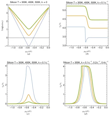
FIG. 3: Dispersion curves for electron-hole oscillations in doped Si (Eg = 1.12eV, me = 0.26m0
and mh = 0.36m0 with m0 being the free electron mass). Panels show the dispersion curve for
various values of electron chemical potential. The normalization factors are r1 = 10−4cm and
ω1 = √
4πe2n
0/m0 with n0 = 1012cm−3. The solid and dashed profiles correspond to Langmuir
and acoustic-like mode, respectively.
plasmas using a collective Schr¨odinger model [45]. In classical pair plasmas, however, the acoustic branch is heavily damped [44] due to phase-mixing of particles.
in P-type Si with µe0 = −0.6eV. As the electron chemical potential value is increased (the sample becomes N-type by introducing donor atoms like As) by going from plot (a) via (b) to (d) with µe0 =−0.5eV, it is seen that the two branches have almost equal frequencies at
k ≈0.12r1−1. This proximity of the modes can become even more pronounced as the Fermi level approaches the valence band. Similar effects have been reported in other studies on pair-charged plasmas [40, 42].
Figure 4(a) shows the cutoff frequency at k = 0 for the electron-hole Langmuir branch in Si with respect toµe0for different values ofT. The frequency has a minimum at the mid-gap for all temperatures. It is also observed that in both N-type (µe0 > −0.56eV) and P-type (µe0 < −0.56eV) Si the frequency increases exponentially with |µe0+ 0.56eV|. Figure 4(b) shows the plateau-like variation of the group speed (with respect to the electron equilibrium chemical potential) for the acoustic-like branch fork = 0.1r−11 at different values ofT. Here, the group speed increases for all values of µe0 (equivalently the doping concentration) with increasing temperature. It is also seen that the group speeds of the acoustic-like oscillations are higher in the P-type region compared to the N-type region (This feature is directly related to the effective masses of electrons and holes, where, for higher electron effective mass semiconductors the group speeds of the acoustic-like oscillations are higher in the N-type region compared to the P-type region). This shows the asymmetrical behavior of electron-hole oscillations in regions with different doping types. It is further observed that the group speed of the acoustic-like branch is nearly independent of µe0 at each semiconductor doping region. In Fig. 4(c), we show the group speed of the Langmuir branch versus µe0 for
IV. THE STATIC CHARGE SHIELDING BY ELECTRONS AND HOLES
Let us now study the static limit of the dielectric function of an electron-hole liquid for arbitrary doping and finite temperature. In doing so, we use the low-frequency kinetic corrected quantum hydrodynamic model as given in Ref. [33] and the isothermal EoS (7). Using the identity ∇Ps(is)=±ns∇µs, the set of closed hydrodynamic equations for electron
and hole species read
0 =±e∇ϕ∓ ∇µs+
ξs¯h2
6m∗s∇
(∇2√
ns
√
ns
)
, (19a)
∇2ϕ= 4πe[n
e−nh+N −Zδ(r)], (19b)
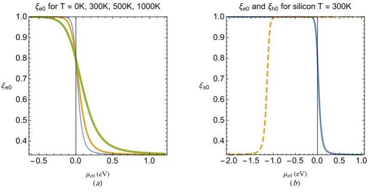
where Z is the charge state of the test charge, δ(r) is Dirac’s delta-function and the zeroth order low-frequency correction factor to the Bohm diffraction term is given by
ξs0 =
Li3/2[−exp (±βµs0)] Li−1/2[−exp (±βµs0)] Li1/2[−exp (±βµs0)]2
. (20)
Figure 5(a) shows the variation ofξe0 versusµe0for different values ofT. For a given value of
T, the value ofξe0 decreases from the limiting classical value ofξs0 = 1 forβµe0 ≪ −1 to the limiting fully degenerate valueξs0 = 1/3 forβµe0 ≫1. However, for−Eg ≤µs0 ≤0 we have 0.795≤ξe0 ≤1 for all temperatures and semiconductor gap-energies. The step-like vertical profile in Fig. 5(a) indicates the value of ξe0 as a function of µe0 at T = 0. Figure 5(b) shows the ξe0 (solid curve) and ξh0 (dashed curve) at T = 300 K. Linearizing and Fourier analyzing the system of Eqs. (19), we arrive at the static dielectric function
Dξ(k,0) = 1 +χe+χh, (21)
where the electron and hole susceptibilities are given by
χs =
ω2
ps
ξs0¯h2k4/(12m∗s2) +v2T sk2
, (22)
and we introduced the generalized thermal speed
vT s =VT s
√
Li3/2[−exp(±βµs0)] Li1/2[−exp(±βµs0)]
, VT s =
√
kBT
m∗s (23)
For the case of highly doped N-type (Nd ≫Na) and P-type (Na ≫Nd) semiconductors, it
simplifies significantly in these limiting cases, and we obtain, respectively,
DN hd(k,0)≃1 +
ω2
pe
ξe0¯h2k4/(12m∗e2) +v2T ek2
, (24a)
DP hd(k,0)≃1 +
ωph2 ξh0¯h2k4/(12m∗h
2) +v2
T hk2
. (24b)
The corresponding screening potential is of the general form [23]
ϕ(r) = Ze 2π2
∫
exp(ikr)
k2D(k,0)d 3
k = Ze 2r
[
(1 +b)e−k+r+ (1−b)e−k−r]
. (25)
The potential given in Eq. (25) with the dielectric function given by either Eq. (24a) or (24b) is known to admit repulsive and attractive forms [36]
ϕr(r) = (Ze/r) exp(−Ar) [cosh(Br) +bsinh(Br)], ηs<
1
4, 1< b <∞, (26a)
ϕa(r) = (Ze/r) exp(−A′r) [cos(B′r) +b′sin(B′r)], ηs>
1
4, 0< b
′ <∞, (26b)
where the parameters are defined as
A=k0s
√√
4ηs+ 1
√ 4ηs
, B =k0s
√
1√−√4ηs
4ηs
, b= √ 1 1−4ηs
, (27a)
A′ =k0s
√√
4ηs+ 1
√ 4ηs
, B′ =k0s
√√
4ηs−1
√ 4ηs
, b′ = √ 1 4ηs−1
, (27b)
and ηs=ξs0h¯2ω2ps/(12m∗s
2v2
T s) andk0s =ωps/vT s.
shielding is of main concern in fabrication of integrated semiconductor devices and is impor-tant in the response of semiconductor detectors to external electrostatic or electromagnetic perturbations.
V. SUMMARY
We have presented a QHD theory for the investigation of high-frequency electron-hole oscillations in semiconductors and static charge shielding by electrons and holes by taking into account the kinetic corrections to the finite temperature chemical potential and quantum diffraction effects in the hydrodynamic model. It is found that holes contribute to the dynamics of oscillations and screening in semiconductors as effective as the electron fluid. Examination of the linear dispersion relation shows the appearance of both a Langmuir branch and an acoustic-like branch in the wave spectrum. The acoustic-like mode has some interesting features regarding the asymmetric behavior in N- and P-type semiconductors. An attractive screening potential also exists for some plasma parameters, and the attractive potential is more pronounced in highly acceptor-doped P-type semiconductors than in highly donor-doped N-type semiconductors with similar doping concentration.
VI. ACKNOWLEDGEMENTS
M-AM would like to express many thanks to Dr. A. Phirouznia and Dr. M. Karimi for useful discussions.
[1] C. Hu, Modern Semiconductor Devices for Integrated Circuits (Prentice Hall, Upper Saddle
River, New Jersey, 2010) 1st ed.
[2] K. Seeger, Semiconductor Physics(Springer, Berlin, 2004) 9th ed.
[3] B. Van Zeghbroeck, Principles of Electronic Devices (2011), Chap. 2.5,
http://ecee.colorado.edu/∼bart/book/contents.htm
[4] F. J. Zutavern, A. G. Baca, W. W. Chow, M. J. Hafich, H. P. Hjalmarson, G. M. Loubriel,
A. Mar, M. W. O’malley, and A. G. A. Vawter, in IEEE Conf. Pulsed Power Plasma Science
[5] H. Haug and S. W. Koch,Quantum Theory of the Optical and Electronic Properties of
Semi-conductors (World Scientific, Singapore, 2004).
[6] P. A. Markovich, C.A. Ringhofer, and C. Schmeister, Semiconductor Equations (Springer,
Berlin, 1990).
[7] C. Kittel, Introduction to Solid State Physics, (John Wiely & Sons, New York, 1996), 7th ed.
[8] N. W. Ashcroft and N. D. Mermin,Solid state physics(Saunders College Publishing, Orlando,
1976).
[9] C. L. Gardner, SIAM J. Appl. Math. 54, 409 (1994).
[10] C. L. Gardner, C. Ringhofer, Phys. Rev. E 53, 157 (1996).
[11] D. Bohm, Phys. Rev.85, 166 (1952).
[12] D. Bohm and D. Pines, Phys. Rev. 92, 609 (1953).
[13] D. Bohm and D. Pines, in Plasma Physics, Ed. J. E. Drummond (McGraw-Hill, New York,
1961) Chap. 2, pp. 35–87.
[14] D. Pines, J. Nucl. Energy: Part C: Plasma Phys. 2, 5 (1961).
[15] E. W. Brown, B. K. Clark, J. L. DuBois, and D. M. Ceperley, Phys. Rev. Lett. 110, 146405
(2013).
[16] T. G. White, S. Richardson, B. J. B. Crowley, L. K. Pattison, J. W. O. Harris, and G. Gregori,
Phys. Rev. Lett.111, 175002(2013).
[17] V. Filinov, M. Bonitz, A. Filinov, V. Golubnychiy, Lect. Notes Phys. 739 41 (2007);
arXiv:cond-mat/0611560 [cond-mat.str-el]
[18] Y. L. Klimontovich and V. P. Silin, Doklady Akad. Nauk SSSR 82, 361 (1952); ibid.J. Exp.
Teor. Fiz. 23 151 (1952).
[19] G. Manfredi, Fields Inst. Commun. 46, 263–287 (2005).
[20] N. Crouseilles, P. A. Hervieux, and G. Manfredi, Phys. Rev. B 78, 155412 (2008).
[21] P. K. Shukla and B. Eliasson, Rev. Mod. Phys.83, 885 (2011).
[22] P. K. Shukla and B. Eliasson, Phys. Usp.51, 53 (2010).
[23] P. K. Shukla and B. Eliasson, Phys. Rev. Lett. 108, 165007 (2012); ibid. 108, 219902 (E)
(2012); ibid.109, 019901(E) (2012).
[24] M. Akbari-Moghanjoughi, Phys. Plasmas 22, 022103 (2015);ibid.22, 039904 (E) (2015).
[25] M. Bonitz, E. Pehlke, and T. Schoof, Phys. Rev. E 87, 033105 (2013).
[27] M. Bonitz, E. Pehlke, and T. Schoof, Phys. Rev. E 87, 037102 (2013).
[28] P. K. Shukla,B. Eliasson and M. Akbari-Moghanjoughi, Phys. Scr. 87, 018202 (2013);
doi:10.1088/0031-8949/87/01/018202
[29] M. Bonitz, E. Pehlke, and T. Schoof, Phys. Scr. 88, 057001 (2013);
doi:10.1088/0031-8949/88/05/057001
[30] D. Michta, F. Graziani, and M. Bonitz, Contrib. Plasma Phys. 55, 437 (2015).
[31] Z. Moldabekov, T. Schoof, P. Ludwig, M. Bonitz and T. Ramazanov, Phys. Plasmas 22,
102104 (2015).
[32] F. Haas,Quantum Plasmas: An Hydrodynamic Approach (Springer, New York, 2011).
[33] F. Haas and S. Mahmood, Phys. Rev. E92, 053112 (2015).
[34] D. B. Melrose and A. Mushtaq, Phys. Rev. E82, 056402 (2010).
[35] B. Eliasson and P. K. Shukla, Phys. Scr.78, 025503 (2008).
[36] B. Eliasson and M. Akbari-Moghanjoughi,Finite temperature static charge screening in
quan-tum plasmas (submitted).
[37] A. Juengel, Transport Equations for Semiconductors, (Springer, Berlin 2009).
[38] V. Romano, J. Math. Phys. 48, 123504 (2007).
[39] L. Stanton and M. S. Murillo, Phys. Rev. E 91, 033104 (2015).
[40] A. Esfandyari-Kalejahi, M. Akbari-Moghanjoughi, and B. Haddadpour-Khiaban, Phys.
Plas-mas 16, 102302(2009).
[41] M. Akbari-Moghanjoughi, Phys. Plasmas 17, 052302 (2010).
[42] A. G. Stewart and E. W. Laing, J. Plasma Phys. 47, 295 (1992).
[43] B. Van Zeghbroeck, Principles of Electronic Devices (2011), Chap. 2.3.7,
http://ecee.colorado.edu/∼bart/book/contents.htm
[44] G. P. Zank and R. G. Greaves, Phys. Rev. E 51, 6079 (1995).
[45] Y. Wang and B. Elasson, Phys. Rev. B89, 205316 (2014).
FIG. 4: (a) The long wavelength Langmuir-like branch normalized frequency versusµefor different
temperatures for a Si sample. (b) The group speed of the acoustic-like branch versus µe for
different temperatures and k = 0.1r−11. (c) The group speed of the Langmuir-like branch versus
µe for k= 0.1r−11 and different values of T. (d) The group speed of Langmuir-like branch versus µe for different wavenumbers at T = 300 K. The subregions µe0 < −Eg/2 and µe0 > −Eg/2
correspond to P- and N-type Si regions, respectively. The normalization factors arer1 = 10−4cm,
ω1 =√4πe2n0/m0 with n0 = 1012cm−3 and v1 =r1/ω1. Thicker curves indicate higher values of
[image:17.595.119.493.69.467.2]FIG. 5: (a) The low-frequency kinetic correction prefactorξe0 versusµe0(eV) for different
tempera-tures. The increase in the thickness of solid profile indicates the increase in the temperature values.
The values ofξe0 = 1 andξe0 = 1/3 correspond to the classical non-degenerate and fully-degenerate
[image:18.595.124.487.80.272.2]FIG. 6: Profiles of the static charge screening potential by (a) electrons in highly doped N-type Si,
(b) holes in highly doped P-type Si. (c) The Shukla-Eliasson-type attractive screening by electrons
and holes. The normalization factors used in these plots are r0 = 10−7cm and ϕ0 =Ze/r0. The
increase in thickness of curves in panels (a) and (b) indicate the increase in the corresponding