A New Scheme of Symmetric Multilevel Inverter
with Reduced Number of Circuit Devices
Seyyed Hossein Hosseini
1, Sajad Najafi Ravadanegh
2Masoumeh Karimi
3, Yahya Naderi
1, and Mohammad Reza Jannati Oskuee
21
Faculty of Electrical and Computer Engineering, University of Tabriz, Tabriz, Iran
hosseini@tabrizu.ac.ir, st_ma_karimi@azad.ac.ir
2
Smart Distribution Grid Research Lab., Electrical Engineering Department,
Azarbaijan Shahid Madani University, Tabriz, Iran
s.najafi@azaruniv.edu, m.r.jannati@azaruniv.edu
3Electrical Engineering Department, Islamic Azad University-South Tehran Branch, Tehran, Iran
1Faculty of Electrical and Computer Engineering, University of Tabriz, Tabriz, Iran
y.naderi@tabrizu.ac.ir
Abstract
In this paper, a sophisticated configuration for symmetric multilevel voltage source inverters is proposed. In multilevel inverters, the costs, circuit size so installation space, complexness of control scheme and reliability are directly depended to the amount of circuit devices required. The provided comparison study among proposed inverter, CHB and recently introduced converters, validates that the proposed inverter reduces the requirements for circuit devices, including power semi-conductor switches, IGBTs, diodes, gate driver circuits and DC voltage sources. The given simulation results confirms the feasibleness of the projected modular structure. Also, to approve the practicality of the proposed inverter, a prototype of the proposed topology has been implemented. Finally simulation and experimental results are compared with one another and therefore the provided comparison shows that the obtained results are in sensible agreements.
1. Introduction
With the advance of power semiconductor technology, the power electronic devices are widely used in industry to improve the manufacturing processes and system efficiency. Multilevel inverters was introduced by Nabae et al and since then, they are taken into account as an important device in power conversion process, so that they have successfully created their own way into the industry and academia as one of the popular selections of DC/AC power conversion. Multilevel inverters are basically made up of an array of power semiconductor switches, diodes and DC power supplies. Multilevel voltage source inverter (MVSI) synthesizes the input DC voltage sources to generate a stepwise output voltage. The number of output voltage waveform levels will increase as the number of input DC voltage sources increases, as well the waveform gets closer to sinusoidal. In comparison with 3 level inverters, the sinusoidal waveform of multilevel inverters can offer substantial benefits, including higher power quality, lower harmonic components, better electromagnetic interface, higher amplitude of fundamental component, higher efficiency, lower harmonic distortion, lower switching losses and lower dv/dt, that makes
asymmetric topologies. It is noticeable that asymmetric topology increases the number of output voltage levels compared with the symmetric counterparts on the condition when both of them compose the same number of power devices. Despite the mentioned advantages of multilevel inverter, they suffer from increased number of required circuit equipment. Due to the dependence of overall costs, circuit size, reliability and control complexity on the number of DC voltage sources, semiconductor switches and related gate driver circuits of switches, the number of required circuit devices are important in multilevel inverter structures. Nowadays advanced topologies are developed to reduce the high number of components in multilevel inverters. Various cascaded based multilevel inverter with different topologies have been introduced by now. A novel MVSI, has been reported in [13]. This inverter uses bidirectional switches. Each bidirectional switch consists of two IGBTs and two diodes. If these IGBTs are connected as common emitter, then for each bidirectional switch, only one gate driver circuit is needed. The main novelty of this converter is about the reduced number of switches compared to CHB. This improvement causes a reduction on gate drive circuits. But, this topology encountered with higher peak inverse value (PIV) compared to CHB. The topology presented in [14], uses unidirectional switches. For unidirectional switches the number of gate drivers is equal to the number of switches. The number of switches and gate driver circuits are less than conventional CHB but the total PIV is more. It is known that reducing the number of switches from the conventional inverters imposes an undesired increase in total PIV value. With proper connection of power switches to DC voltage sources, this increase can be limited. Comparatively, the PIV of [14] is reduced considerably to that of [13]. Also it must be mentioned that, since the number of IGBTs, switches and gate driver circuits are reduced significantly, an increase in total PIV is acceptable and can be neglected while this increase cannot detract from its values of obtained benefits from reductions. Recently, a novel MVSI has been suggested, that is reduced the power components [15] compared to CHB. Moreover, this inverter has kept the PIV equal to CHB.
The main contribution of this paper is proposing an advanced configuration for the symmetric multilevel voltage source inverter. This topology is inspired of the idea behind conventional CHB. This inverter reduces the requirements for circuit devices compared to conventional CHB and the recently proposed CHB based inverters in [13-15]. In this regards, the proposed inverter is analyzed and then a full comparison is provided to validate the superiority of the proposed multilevel inverter. The lower number of requirements for circuit devices results lower costs and the installation area, higher reliability and ease of implementation and simpler control scheme. The remainder of this paper is organized as follows: the structure and details of proposed topology are described item by item in section 2. A full comparison between the suggested inverter and the well-known inverters is represented in section 3. Both simulation and experimental outcomes are given in section 4. Finally, section 5 represents the conclusion.
2. Proposed Configuration
Fig. 1(a) shows the basic cell of the proposed multilevel structure. As seen in this figure, the basic unit consists of five semiconductor unidirectional switches and three insulated DC
voltage sources. The proposed cell is symmetric, so, the values of DC sources are equal. Each unidirectional switch includes an IGBT and an anti-parallel fast recovery diode. Each basic unit can generate four levels in its output, contains three positive steps and one zero value. Table 1 indicates switching states of the basic unit of the proposed structure for each output voltage value. In the proposed unit, the related switches must be controlled in order to avoid short circuit. Thus, in this Table, 1 and 0 indicate the on and off states of the switches, respectively. The tantamount circuits for different output voltages of basic unit of the symmetric MVSI are shown in Fig 1 (b)-(d).
Si1
Si3 Si2
Vdc
Si4
Si5
Vdc V
dc
10 pt
(a)
Si1
Si3 Si2
Vdc
Si4
Si5
Vdc V
dc
(b) Si1
Si3 Si2
Vdc
Si4
Si5
Vdc V
dc
(c)
Si1
Si3 Si2
Vdc
Si4
Si5
Vdc V
dc
(d) Si1
Si3 Si2
Vdc
Si4
Si5
Vdc V
dc
(e)
[image:2.595.337.495.190.688.2]Table 1. Various switching states of i-th suggested basic cell
State Si1 Si2 Si3 Si4 Si5 Vo
1 0
1
1
01
3Vdc2 0
1
01
1
2Vdc3
1
01
01
Vdc4
1
01
1
0 0 [image:3.595.53.291.92.169.2]The generalized view of the proposed MVSI is represented in Fig. 2. As shown, the proposed structure contains of series connection of k-basic units, two DC sources, associated with six semiconductor unidirectional switches. The switches of
,
,
,
,
L L
U U
H H M M H and H
are well configured, so that theproposed inverter can generate all the possible voltage steps with the value of positive and negative in the output. The mentioned independent DC voltage sources are pointed by
dc
V
and
s
V . The amplitude of
s
V
that is series with the basic units is set pursuant to the number of required DC voltage sources. And the number of DC sources is depended to the number of output voltage levels. In this regards,s
V can be either zero or any values of
dc
V or
2
V
dc. As illustrated in this figure, the proposed topology is composed by n-isolated DC voltage sources. Rectifiers connected to isolated transformers fed from AC voltage can produce different DC voltage sources [16]. Also, the required DC voltage sources in this structure can be achieved by applying renewable energy sources such as photovoltaic cells or fuel cells, or with energy storage devices, like batteries. It is notable that the proposed MVSI is symmetric, so the required DC voltage links must be equal in values. The quality of the output voltage may be deteriorated due to the inequality of DC voltage sources and as a result of inequality of voltage levels. In this regards, undesired harmonics can be generated in the output voltage. In whatever way, the notable point is that producing balanced DC voltage sources is the same problem among all symmetric inverters. In some cases, supplementary circuits, to provide equal DC voltages, are required for symmetric inverters. For instance, if the PV panels are employed as DC voltage sources, they have already equipped with DC/DC converters for voltage level adjustments. The DC voltage sources can be produced by using transformers and rectifiers. Nevertheless, the undesired changes in the DC voltage sources can be compensated by complementary modulation strategies [17, 18]. The implementation of these methods needs the manipulation of the inverters hardware by additional devices and circuits, and makes the control scheme more intricate. As the proposing a novel structure for multilevel inverters is the main goal of this paper, so countervailing differences of DC voltages which can be done by modulation methods, is not taken into consideration. A provided output phase voltage is the sum of individual voltages of DC power supplies amplitudes. So, the maximum obtainable value for the output voltage (,max
o
V ) of the introduced
MVSI can be calculated by the following equation:
,max 1 n o i i
V
V
(1)where
n
-is the number of DC sources. The number of output voltage levels (m) can be obtained using the following equation:,max
2 o 1
dc
V m
V
(2)
Hl Hl
M M Hu Hu Vdc + Vo -VS Io
ith-Cell kth-Cell 1st-Cell
Individual DC source
R
L
Fig. 2. Proposed MVSI
The
proposed cascaded multilevel inverter is as symmetric inverter. So, increasing the number of cells is the solution to reach a definite value in the numbers of output voltage levels. Inorder to clarify the proposed inverter’s characteristics, it is
needed to specify the parameter
L
.L
is an integer number and1, 2,3,...
L
. It is obvious that to generate m-levels in the output voltage, n-DC sources are needed. That is:1
; 6 3 2
1
; 6 5 2
1
1; 6 7 2
m
if m L
m
n if m L
m
if m L
(3)
Since each cell consists of three DC voltage sources, so with n
DC links, it is possible to have
k
basic cells. It is clear that, inthis configuration n must be in a proper relationship with
k
. So:1
; 6 3 3
2 ; 3
n if m L
k n otherwise (4)
As said before, the value of
s
V
is set according to the number of output voltage levels. In the following the relationship betweens
V and
m
is mathematically formulated:0 6 3
6 5
2 6 7
S dc
dc
if m L
V V if m L
V if m L
(5)
For simplicity, when it is required to generate
m
-levels in output voltage, the number of required DC sources must be obtained using (3) and the value ofs
V
must be chosen according to the given formula in (5). For instance to generate 9-levels in output voltage, the number of DC links is four and thens
V
is set to be zero. Also, for m11and13 the number of DC voltage sources is calculated to be five. And thens
be 2
s dc dc
V V and V , respectively. In the suggested inverter, the number of switches (
switch
N ) is calculated by (6):
5 13
; 6 3 3
5 8 ; 3
Switch
n
if m L
N
n
otherwise
(6)
Moreover, the equation between the number of output levels (
m
) and the number of switches (switch
N ) is as follows:
5 21
; 6 3
6 5 11
; 6 5
6 5 1
; 6 7
6
Switch
m if m L
m
N if m L
m
if m L
(7)
Each switch requires a separate driver circuit to produce switching pulses, thus the number of driver circuits is equal to the number of power switches, too. So:
Driver switch
N
N (8)The total peak inverse voltagePIV of switches is the other essential parameter of the inverter which is calculated as follow:
1
Switch j
N
Switch j
PIV PIV
(9)
So, the below formulations are used to calculate the total PIV:
. .
19 7
; 6 3
3 3 19 14
; 6 5
3 3 19 2
; 6 7
3 3
p u
n if m L
n
PIV if m L
n
if m L
(10)
In symmetric mode, the relationships between PIV and
m
is formulated as follows:. .
19 33
; 6 3
6 19 47
; 6 5
6 19 61
; 6 7
6
p u m
if m L
m
PIV if m L
m if m L
(11)
3. Comparison of the Proposed Inverter with
Other Multilevel Inverters
Generating the specific number of output voltage levels by using less number of circuit devices is the main goal of introducing the proposed symmetric structure. The purpose of this section is to compare the major parameters such as IGBTs, gate driver circuits, DC voltage sources and total PIV among the proposed multilevel inverter and the conventional symmetric MVSIs reported in literatures. Comparing the proposed inverter with symmetrical inverters is fair and rational. It is pointed out that the proposed inverter is indicated by P and the other symmetric inverters participated in comparison study are shown by R1–R4 in these comparisons. The conventional symmetric
cascaded H-bridge inverter is refereed to as R1. The proposed system of [15] is R2, while R3 is related to [13]. Fianlly, the
system in [14] is referred to as R4. The comparison of MVSI’s is
discussed versus output voltage levels. In this regards, it is assumed that the maximum output voltage is equal for all mentioned inverters. The numbers of IGBTs versus the number of voltage levels for various MVSI configurations are
represented in Fig. 4. The proposed inverter uses unidirectional switches, then the number of gate drivers is equal to Nswitch.
[image:4.595.311.531.170.287.2]However, R3, has several bidirectional switches in its topology. Each bidirectional switch consists of two IGBTs. Since these IGBTs are connected as common emitter, then for each bidirectional switch, only one gate driver circuit is needed. Assuming this concept, the number of gate driver circuits versus output voltage levels are shown in Fig. 5.
[image:4.595.306.536.323.428.2]Fig. 3.Number of IGBTs versus number of levels for proposed topology and other mentioned solutions
Fig. 4.Number of gate driver circuits versus number of levels for proposed topology and other mentioned solutions
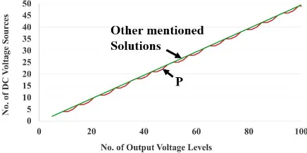
Regarding Figs. 3&4, in the all range of possible voltage levels, the proposed topology reduces the requirements for IGBTs and gate driver circuits in comparison with other mentioned solutions. Therefore, less components result in reduction in the required installation area and the costs. Also, the control scheme gets simpler and the reliability of overall system is enhanced as well. The number of required DC voltage sources is another parameter plays a key role on overall inverter costs. Fig. 5 shows the number of DC voltage sources versus output levels in all mentioned inverters.
[image:4.595.312.530.584.693.2]By considering the above Figs., it can be understood that in order to achieve the same level in the output, the number of required DC voltage sources in the proposed symmetric inverter is mostly keeps close to other presented structures and in some output levels is lower. Another essential parameter which plays a consequential role on overall inverter expense is the voltage ratings of power switches. It is known that reducing the number of switches from the conventional inverters imposes an undesired increase in total PIV value. With proper connection of power switches to DC voltage sources, this increase can be limited. Fig. 6 depicts the value of considered inverters.
Fig. 6.Total PIV value versus number of levels for proposed topology and other mentioned solutions
Because of the big reduction in circuit equipment in the proposed inverter, a bit increase in its total
PIV
compared to some conventional inverters is acceptable and can be neglected, while a reduction in number of switches, gate driver circuits and DC power supplies are achieved.4. Simulation and Experimental Results
In order to verify the correct performance of the proposed
multilevel inverter in generating all output voltage levels,
the both simulation and experimental results have been
provided. The converter is simulated by
MATLAB/Simulink software. Then, to validate the
practicability and the good performance of the suggested
MVSI, experimental results are obtained and compared
with those of simulation ones. To provide the DC voltage
links, the adjustable DC sources existing in the
laboratory, have been used. Table 2 represents the main
parameters of implemented circuit.
Table 2. Parameters of the implemented inverter.
Type of switch IRF260
Type of MOSFET driver Hcpl316j
Pulse Generator AVR mega 32
DC Voltage Sources Magnitudes Vdc30V Series R-L Load Parameters 30 Ohm & 20mH
Fundamental Frequency 50Hz
Different switching strategies are introduced to improve the quality of output voltage waveform. For instance, fundamental frequency-switching, sinusoidal PWM, selective harmonic elimination (SHE-PWM), space vector PWM (SV-PWM), and others are such the modulation techniques that apply for this
purpose. The fundamental frequency-switching scheme is applied in this study because of low switching frequency of it [19]. For power converters, the total harmonic distortion (
THD
) is an important indicator that evaluates the quantity of harmonic contents in the output waveform. The THD is defined as follows: The ratio of the sum of the RMS value of power of all harmonic components to the RMS value of power of the fundamental frequency component is defined as THD. So the following equation gives the THD value.1 1
2 2
2
1
on
rms
o n
o o
V
V THD
V V
(12)
In this equation,
n
-represents the order of the corresponding harmonic, while the sub-index 1 corresponds to the fundamental frequency. Hence,n o
V
and1 o
V
are the rms of then
order harmonic and fundamental of the output voltage, respectively. Also,rms
o
V represents the rms magnitudes of the output voltage.
In above relation, the value of
1 o
V
andrms o
V
can be obtained using the following equations, respectively:2
1,3,5,... 1 cos 2 2
( )
Level rms
N
dc
j
j
m
o V
m m V
(13)
1
1 2 2
cos
Level
o j
N
dc j
V V
(14)
Where, the values of 1
,
2,...
Level
N
represent switching angles and is calculated by:
1 0.5
sin ( ) j 1, 2,3,...
j Level
Level
j
N N
(15)
It is clear that the value of THD depends on the number of levels and so, switching angles. It is important to mention that removing the selective harmonics and reducing the total harmonic distortion are not the goal of the presented paper. And this switching scheme is only used to generate the desired voltage steps. Fig. 7 shows the circuit diagram of the 11-Level multilevel inverter.
l l
u u
dc
o o
dc 1
3 2
4 5
dc
[image:5.595.321.531.504.639.2]dc dc Basic Cell
Fig. 7. Circuit diagram of 11-Level multilevel inverter
Table 3. Switching states of proposed symmetric 11-level inverter
Output
Voltage Hl M S1 S2 S3 S4 S5 Hu 5
dc
V 011110
4
dc
V 111110
3
dc
V 010--0
2
dc
V 110--0
dc
V 01---1
0 00---0/11---1
-dc
V 10---0
-2
dc
V 001—1
-3
dc
V 101—1
-4
dc
V 000001
-5
dc
V 100001
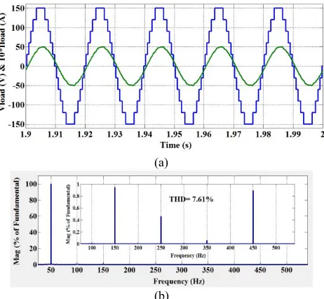
The voltage and current waveform of the simulated 11-level proposed inverter are shown in Fig. 8.
(a)
[image:6.595.85.261.93.282.2](b)
Fig. 8. a) Voltage and current waveforms and b) harmonics content of voltage of the proposed 11-level inverter
As it can be seen, all the voltage levels can be generated in the suggested inverter which validates the practicability of proposed inverter. To confirm the feasibility of the suggested multilevel inverter, the measured output voltage and current waveforms of implemented single phase prototype of the 11-level proposed inverter are shown in Fig. 9 (a) and (b).
(a)
(b)
Fig. 9. Experimental results of implemented 11-level proposed inverter. a) Output voltage (no load), b) output voltage and
current.
The provided results confirm that the proposed inverter is able to generate the desired output voltage waveform. These figures show good agreements in the simulation and experimental results. The negligible difference between the magnitudes of the simulation and experimental results is due to voltage drops on switches in the prototype.
5. Conclusions
The main purpose of this paper is to propose an advanced structure for symmetric multilevel voltage source inverters. This novel modular configuration applies reduced number of circuit devices, such as its power switches, diodes, IGBTs, gate driver circuits of switches and DC voltage sources. The lower number of needed circuit equipment results remarkable reduction in general costs and installation area, improved reliability and simpler control procedure.
In order to demonstrate the performance of the proposed inverter over the conventional CHB and recently proposed symmetric inverters a full comparison study is provided. Also, a prototype of the proposed topology has been implemented to validate the practicability of the recommended structure. At the end of the paper, the provided simulation and experimental results are compared with each other to demonstrate the good compromise of the achieved results.
CH1: 50V/div
Time: 2.5ms/div
[image:6.595.60.291.323.536.2]6. References
[1] M.R. Banaei, M. R.J. Oskuee and F.M.Kazemi, “A New Advanced Topology of Stacked Multicell Inverter”, Int. J. of Emerging Electric Power Syst., 2014; 15(4), pp. 327–333.
[2] M.R.J. Oskuee, M. Karimi, S.N. Ravadanegh, and G.B.
Gharehpetian, “An Innovative Scheme of Symmetric Multilevel Voltage Source Inverter with Lower Number of Circuit Devices,” IEEE Trans.
Ind. Electronics, vol. 62, no.11, Aug. 2015
[3] M.R. Banaei, M.R.J. Oskuee, F.M. Kazemi, “Series H-bridge with stacked multicell inverter to quadruplicate voltage levels”, IET Power Electron., 2013, Vol. 6, Iss. 5, pp. 878–884
[4] E. Babaei, S.H. Hosseini, “New cascaded multilevel inverter topology with minimum number of switches”, J. Energy Convers. Manag., vol. 50, no. 11, pp. 2761–2767, 2009
[5] M.R. Banaei, M.R.J. Oskuee, and H. Khounjahan,“Reconfiguration
of semi-cascaded multilevel inverter to improve systems performance
parameters,” IET Power Electron., vol. 7, no. 5, pp. 1106 – 1112, May 2014.
[6] E. Babaei, S.H. Hosseini, G.B. Gharehpetian, M. Tarafdar Haquea,
M. Sabahi, “Reduction of dc voltage sources and switches in
asymmetrical multilevel converters using a novel topology”, Electric
Power Systems Research vol. 77, pp. 1073–1085, 2007
[7] Y. Hinago, and H. Koizumi, “A Single-Phase Multilevel Inverter
Using Switched Series/Parallel DC Voltage Sources”, IEEE Trans. Ind. Electrons, vol. 57, no. 8, pp. 2643-2650, Aug. 2010
[8] W.-K. Choi, and F.-S. Kang. "H-bridge based multilevel inverter using PWM switching function." Telecommunications Energy Conference, 2009. INTELEC 2009. 31st International. IEEE, 2009. [9] A. Ajami, B. Mohammadzadeh, and M.R.J. Oskuee, “Utilizing the
Cuckoo Optimization Algorithm for Selective Harmonic Elimination
Strategy in the Cascaded Multilevel Inverter”, ECTI Trans. on Elec. Eng., Electr, and Comm. vol.12, no.1, pp. 8-16, Feb. 2014
[10] S. Das, G., and M. Pandey, “Space-Vector-Based Hybrid Pulse width Modulation Techniques for a Three-Level Inverter,” IEEE Trans.
Power Electron, vol. 29, no. 9, pp. 4580 - 4591, Apr 2014.
[11] E.S. Deepak, C.S: Anil, S. Sanjay, C. Febi, K.R. Sajina, "A novel multilevel inverter topology based on multi-winding multi-tapped transformers for improved wave shape requirements," Power Electronics (IICPE), 2010 India International Conference on , vol., no., pp.1,5, 28-30 Jan. 2011
[12] S. Kouro, M. Malinowski, K Gopakumar, J. Pou, L.G. Franquelo, W. Bin; J. Rodriguez, M.A. Perez, J.I. Leon, J.I., "Recent Advances and Industrial Applications of Multilevel Converters," Industrial Electronics, IEEE Transactions on , vol.57, no.8, pp.2553,2580, Aug. 2010
[13] E. Babaei, S.H. Hosseini, G.B. Gharehpetian, M. T. Haquea, M.
Sabahi, “Reduction of dc voltage sources and switches in asymmetrical
multilevel converters using a novel topology,” Electric Power Systems
Research , vol. 77, no. 8, pp. 1073–1085, Jun. 2007
[14] Y. Hinago, and H. Koizumi, “A Single-Phase Multilevel Inverter
Using Switched Series/Parallel DC Voltage Sources,” IEEE Trans. Ind.
Electrons. , vol. 57, no. 8, pp. 2643-2650, Aug. 2010.
[15] A. Ajami, M.R.J. Oskuee, M.T. Khosroshahi, A. Mokhberdoran,
“Cascade-multi-cell multilevel converter with reduced number of
switches,” IET Power Electron., 2014, Vol. 7, Iss. 3, pp. 552–558, Mar. 2014
[16] E. Babaei, “Optimal topologies for cascaded sub-multilevel
converters,” J. Power Electron., vol. 10, no. 3, pp. 251–261, 2010. [17] V. Naumanen, J. Luukko, P. Silventoinen, J. Pyrhonen, H. Saren, and K. Rauma, “Compensation of DC link voltage variation of a multilevel series-connected H-bridge inverter,” IET Power Electron.,
vol. 3, no. 5, pp. 793–803, Sep 2010.
[18] S: Lu, S: Mariethoz, and K.A. Corzine, “Asymmetrical cascade
multilevel converters with noninteger or dynamically changing DC voltage ratios: concepts and modulation techniques,” IEEE Trans. Ind. Electronics, vol. 57, no. 7, pp. 2411–2418, Jun 2010.