University of Southampton Research Repository
ePrints Soton
Copyright © and Moral Rights for this thesis are retained by the author and/or other copyright owners. A copy can be downloaded for personal non-commercial
research or study, without prior permission or charge. This thesis cannot be
reproduced or quoted extensively from without first obtaining permission in writing from the copyright holder/s. The content must not be changed in any way or sold commercially in any format or medium without the formal permission of the
copyright holders.
When referring to this work, full bibliographic details including the author, title, awarding institution and date of the thesis must be given e.g.
AUTHOR (year of submission) "Full thesis title", University of Southampton, name of the University School or Department, PhD Thesis, pagination
UNIVERSITY OF SOUTHAMPTON
FACULTY OF ENGINEERING, SCIENCE &
MATHEMATICS
OPTOELECTRONICS RESEARCH CENTRE
Thiolate self-assembled monolayers
studied with a Tuneable Infrared Low
Temperature Laser Driven Scanning
Tunnelling Microscope
by
Howard John Millman
A thesis submitted to the University of Southampton for the degree of Doctor of Philosophy.
ii ABSTRACT
FACULTY OF ENGINEERING, SCIENCE AND MATHEMATICS OPTOELECTRONICS RESEARCH CENTRE
Doctor of Philosophy
Thiolate self-assembled monolayers studied with a Tuneable Infrared Low Temperature Laser Driven Scanning Tunnelling Microscope.
By Howard John Millman
This work describes the investigation of self-assembled monolayers (SAMs) with scanning tunnelling microscopy/spectroscopy (STM/S) and infrared laser-driven STM (LDSTM). As a tool STM is uniquely able to resolve atoms on a surface. Illuminating an STM with infrared radiation tuned to match modes in the SAM used as the sample provides a unique opportunity to investigate the combination of the well understood character of organic molecules with the atomic scale resolution of an STM.
SAMs were prepared with octanethiol and dimethyl disulphide on Au(111) substrates. STM images and STS spectra of these samples recorded at 78K are presented. Typical surface features are observed in the octanethiolate monolayers. The results of STS experiments with an octanethiolate monolayer reveal correlations between surface features and conductivity at -1.0V. The differences between these STS data and equivalents from uncoated samples reveal the effect of the molecules upon the electronic surface states of the samples. Images of samples prepared with dimethyl disulphide show previously unseen low density structures and individual molecules scattered across the surface. Correlations are made between these low density structures and the reconstruction of the underlying gold surface. Comparisons with previously calculated models are used to identify these isolated molecules. STS data collected across a section of sample show how topography data can be used to categorise STS data.
iii
I, HOWARD JOHN MILLMAN declare that the thesis entitled:
“Thiolate self-assembled monolayers studied with a Tuneable Infrared Low
Temperature Laser Driven Scanning Tunnelling Microscope”
and the work presented in it, are my own.
I confirm that:
this work was done wholly or mainly while in candidature for a research
degree at this University;
where any part of this thesis has previously been submitted for a degree or
any other qualification at this University or any other institution, this has
been clearly stated;
where I have consulted the published work of others, this is always clearly
attributed;
where I have quoted from the work of others, the source is always given.
With the exception of such quotations, this thesis is entirely my own work;
I have acknowledged all main sources of help;
where the thesis is based on work done by myself jointly with others, I
have made clear exactly what was done by others and what I have
contributed myself;
none of this work has been published before submission.
Signed: ...
iv Despite only having one name on the cover, this thesis would not have been possible without the input of others whose assistance has been invaluable.
Firstly a huge thanks to Dr. Naruo Yoshikawa who enabled this project to progress much faster than it otherwise might have and taught me virtually everything I know about UHV systems. Thanks to Dr. Peter Stone for starting the work with the LTSTM and getting us up to speed with its operation. Thanks to Dr. Lefteris Danos for assisting me in starting the work with the OPO and to Dr. Martin O’Connor for his insightful advice.
A big thanks to Dr. Bill Brocklesby and Dr. Jeremy Frey for coming up with the crazy idea to do this and keeping watchful eyes over the whole project. Thanks to the EPSRC for paying for all of this.
Thanks to Prof. Brian Hayden and the various past and present members of his group for advice and assistance in the laboratory and all things UHV related. Specifically thanks to Dr. Mike Rendall for teaching me everything else about UHV that Dr. Yoshikawa did not and for various IT skills that I have found invaluable; thanks to D. Scott Bazley and Ben Wilkinson for their assistance in manhandling the LTSTM and thanks to Duncan Smith for the use of the infrared camera which made beam alignment a lot less painful.
Huge thanks to Jamie Robinson and Kieron Taylor for their programming knowledge and assistance. I owe you several instances of $BEVERAGE. Thanks to Esther Rousay and Adrian Wiley for the Perl script to generate Figure 1.1.
Thanks to my family for starting me off on this journey of scientific discovery and being there along the way. Thanks to Suzanne Elliman for allowing me the time to finish this work.
Finally the greatest thanks must go to הוהי
v
Abbreviations
AC - alternating current
AFM - atomic force microscope/microscopy BCC - body centred cubic
DC - direct current DMDS - dimethyl disulphide
FCC - face centred cubic
FEG-SEM - field emission gun scanning electron microscope FTIR - Fourier transform infrared (spectroscopy)
HOPG - highly oriented pyrolytic graphite IETS - inelastic tunnelling spectroscopy
LDAFM - laser driven atomic force microscope/microscopy
LDSTM - laser driven scanning tunnelling microscope/microscopy LEED - low energy electron diffraction
LTSTM - low temperature scanning tunnelling microscope/microscopy OPO - optical parametric oscillator
SAM(s) - self-assembled monolayer(s)
SEM - scanning electron microscope/microscopy SNOM - scanning near field microscope/microscopy
SPM - scanning probe microscope/microscopy STM - scanning tunnelling microscope/microscopy
STS - scanning tunnelling spectroscopy TISE - time-independent Schrödinger equation
TSP - titanium sublimation pump UHV - ultra-high vacuum
vi
Acknowledgements iv
Abbreviations v
Contents vi
List of Figures x
1 Chapter 1: Introduction 1
1.1 Chapter Introduction 2
1.2 Overview of the Work 5
1.3 Outline of Thesis 5
1.3.1 Chapter 1: Introduction 5
1.3.2 Chapter 2: Technologies and Techniques Used 5 1.3.3 Chapter 3: Scanning Tunnelling Microscopy Tips 6
1.3.4 Chapter 4: Au(111) Samples 6
1.3.5 Chapter 5: Thiol Self-Assembled Monolayers 7 1.3.6 Chapter 6: Laser Driven Scanning Tunnelling 7
Microscopy Experiments 7
1.3.7 Conclusions 7
1.4 References 8
2 Chapter 2: Techniques and Technologies Used 10
2.1 Chapter Introduction 11
2.2 Scanning Tunnelling Microscopy 11
2.2.1 A Brief History 11
2.2.2 An Overview of STM 13
2.2.3 A Theoretical Approach 14
2.2.3.1 The Rectangular Barrier 15
2.2.3.2 The Barrier Height (Workfunction) 19
2.2.3.3 The WKB Model 21
2.2.3.4 The Tersoff and Hamann Model 24
2.2.4 STM Spectroscopy 28
2.2.5 STM Equipment 34
vii
2.3.1 Overview 45
2.3.2 Background & Theory 46
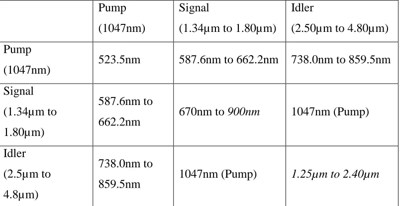
2.3.3 Specific Details of the OPO Used for This Work 50
2.4 Self-Assembled Monolayers 57
2.5 Laser-Driven Scanning Tunnelling Microscopy (LDSTM) 60
2.5.1 Thermal Effects 61
2.5.2 Other LDSTM Responses 64
2.6 Chapter Summary 66
2.7 References 66
3 Chapter 3: The Manufacture and Imaging of Scanning Tunnelling
Microscopy Tips 74
3.1 Chapter Introduction 75
3.2 Experimental Methods Used 75
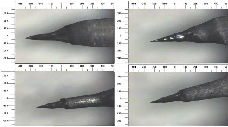
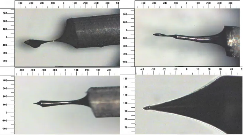
3.3 Results and Discussion 76
3.3.1 Optical Microscope Images of STM Tips 76 3.3.1.1 Tungsten Tips Etched with Alternating Current 76 3.3.1.2 Tungsten Tips Etched with Direct Current 79
3.3.2 FEG-SEM images of STM tips. 81
3.3.3 STM Images Produced With Etched STM Tips 85
3.4 Conclusions and Future Work 86
3.5 References 87
4 Chapter 4: Au(111) Surfaces 90
4.1 Chapter Introduction 91
4.2 Preparing Au(111) Surfaces 91
4.2.1 Experimental Method 91
4.2.2 Results and Discussion 93
4.3 Spectroscopy of Au(111) Surfaces 96
4.3.1 Experimental Methods 96
4.3.2 Results and Discussion 97
4.4 Conclusions 100
4.5 Further Work 101
viii
5.1 Chapter Introduction 105
5.2 Octanethiol on Au(111) 106
5.2.1 Preparation of Octanethiol Self-Assembled Monolayers 106
5.2.1.1 Experimental Method 106
5.2.1.2 Results and Discussion 107
5.2.2 Spectroscopy Experiments with Octanethiol on Au(111) 113
5.2.2.1 Experimental Methods 113
5.2.2.2 Results and Discussion 114
5.3 Dimethyl Disulphide on Au(111) 121
5.3.1 Preparation of Dimethyl Disulphide
Self-Assembled Monolayers 121
5.3.1.1 Experimental Method 121
5.3.1.2 Results and Discussion 123
5.3.2 Spectroscopy Experiments
of Dimethyl Disulphide on Au(111) 129 5.3.2.1 Topographically Varying Scanning Tunnelling Spectroscopy 130 5.3.2.1.1 Experimental Method 130 5.3.2.1.2 Results and Discussion 130 5.3.2.2 Scanning Tunnelling Spectroscopy Conducted on a Complete Monolayer 133 5.3.2.2.1 Experimental Method 133 5.3.2.2.2 Results and Discussion 133
5.4 Conclusions 136
5.5 Future Work 139
5.6 References 140
6 Chapter 6: Laser Driven Scanning Tunnelling Microscopy 142
6.1 Chapter Introduction 143
6.2 Experimental Methods 143
6.2.1 General Principles 143
6.2.2 Specific Procedures Used 146
6.2.2.1 Laser Modulation Frequency 148
ix
6.2.2.5 Laser Wavelength 150
6.2.2.6 Chemical Nature of the Sample 150
6.2.2.7 Surface Topography 150
6.3 Results and Discussion 151
6.3.1 Laser Modulation Frequency
and Applied Tunnelling Voltage 151
6.3.2 STM Electronics 153
6.3.3 Tunnelling Current 155
6.3.4 Chemical Nature of the Sample 157
6.3.5 Laser Wavelength 158
6.4 Conclusions and Future Work 160
6.5 References 163
7 Chapter 7: Conclusions 165
7.1 References 169
A Appendix A: Manufacture of STM Tips 171
B Appendix B: Etching Circuit Diagrams 173
C Appendix C: Microscope Images of the PPLN OPO Crystals 175
D Appendix D: MATLAB® Code for Processing Topographically Varying ||
Scanning Tunnelling Spectroscopy Data 176
E Appendix E: MATLAB® Code for Processing Scanning Tunnelling |||||||
x
Figure Caption Page
1.1 An example a self-assembled monolayer of methanethiolate on gold. This cartoon is based upon a unit cell by De Renzi et al.[6] used for calculating the positions of the thiolate species on the surface.
3
2.1 Schematic of the tunnelling set-up. A very sharp metal tip is positioned very close to the surface and a voltage is applied between the two, as the tip is raster scanned across the surface whilst the current is measured.
13
2.2 Illustrating the simple case of tunnelling through a rectangular shaped barrier. The electron is considered to travel from the left to the right along the x axis. Between x = 0 and x = L there is a potential barrier with a height of energy V0.
15
2.3 Showing a wavefunction tunnelling through a barrier of arbitrary shape. This scenario can be described with the WKB model but only if the electron energy is not near the height of the barrier.
21
2.4 The WKB approximation can be made to work when the electron energy is close to the barrier height if a linear barrier is used. Removing the restriction on the electron energy comes at a cost of only being able to use a barrier with a linear shape.
21
2.5 Typical relative sizes of 5dz² and 6s orbitals in atoms in the tip. Doyen suggests that the radius of the 6s orbital is too large to explain the atomic resolution seen in some STM images.
27
2.6 Schematic STS curves showing how they are affected by a vibrational mode on a surface. The gradient of the I vs. V curve increases when the electron energy matches the energy of the vibrational mode. Such a change in the I vs. V curve will lead to
dV
dI vs. V and 2 2 dV I
d vs. V curves with shapes as shown. The symmetry of these curves is due to the fact that the interaction of the mode with the tunnelling electrons is independent of the
xi an example of how the number of measurements recorded is
adequate to lower the signal to noise ratio.
2.8 A stylised diagram showing some of the components of the LTSTM.
35
2.9 Photograph of the STM head unit. The piezoelectric stack is in the centre of the image. A tip holder (with tip) would sit on top of it in the place marked by the blue dot. The silver vertical rods to the left, right and rear (obscured) can be lowered such that the head detaches from the inner cryostat at the places marked with the blue line and becomes suspended on springs.
36
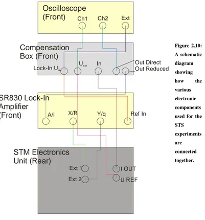
2.10 A schematic diagram showing how the various electronic components used for the STS experiments are connected together.
39
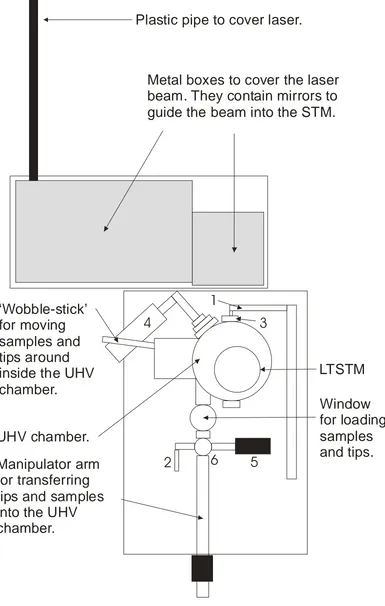
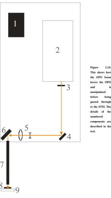
2.11 A highly stylised plan of the rig. Descriptions of the numbered components are included in the text.
40
2.12 Showing how the thermocouple and resistive heater are used with the manipulator arm to gently heat samples. The shaded cylinder represents the screw thread which can be moved in the direction shown by the arrow to raise and lower the resistive heater (dark loop protruding from the cylinder) and the thermocouple wire (thin line protruding from the cylinder). The loop of resistive heating wire is narrow enough to fit between the two parallel tungsten rods. (This figure is based upon Figure 20 from the Multiprobe® Surface Science Systems User’s Guide Version 1.5, OMICRON Vakuumphysik GmbH. Used with permission.)
41
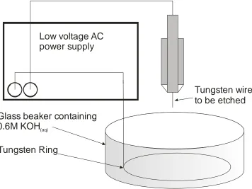
2.13 Diagram of the AC tip etching apparatus. 43 2.14 Close-up photograph of the beaker, tungsten ring and wire, shown
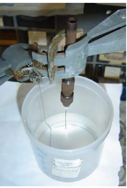
in the previous Figure showing how the wire is positioned with respect to the ring.
43
2.15 A schematic diagram of the apparatus used for DC etching. 44 2.16 Showing the plastic beaker and smaller stainless ring used for DC
etching.
xii with different types of phasematching.
2.18 Stylised representation of a mask used for the poling of a lithium niobate crystal. Here are shown three sets of gratings each with a different period spacing to provide a tuning capability for the OPO. This mask would be placed on the side of a lithium niobate crystal and a high voltage applied across the crystal through the mask.
49
2.19 This is a stylised representation of the top grating in a Periodically Poled Lithium Niobate (PPLN) crystal made with the above mask and viewed from above. The arrows and shading indicate the orientation of the optical axis in the crystal.
49
2.20 Schematic showing the layout of the OPO 51 2.21 Photograph of the OPO used in this work. The coloured arrows
show the paths of the different beams travelling through the OPO. The green arrows correspond to the path of the incident pump beam. The blue arrows as in Figure 2.19 show the path of the signal photons though the cavity. The orange arrow shows the path of the output beam from the OPO which contains components at several wavelengths
51
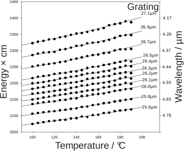
2.22 Showing how by using different gratings in PPLN crystal 1 at different temperatures the OPO can emit a wide range of wavelengths.
53
2.22 Showing how by using different gratings in PPLN crystal 2 at different temperatures the OPO can emit a wide range of wavelengths.
53
2.24 This shows how the OPO beam leaves the OPO and is manipulated before being passed through to the STM. The details of the numbered components are described in the text.
56
2.25 A stylised representation of octanethiol molecules lying flat on an Au surface at low surface coverage. The diagonal zigzag lines are the carbon chains, the yellow S’s are the sulphur atoms and the horizontal wavy line is the metal surface.
xiii top left.) (Scales are in microns.)
3.2 Examples of AC etched macroscopic double tips. (Scale is in microns.)
77
3.3 AC manufactured tips showing changes in the tip angle part way down the tip cone. (Scales are in microns.)
78
3.4 An example of an AC etched tip with a multi-step tip shape. (Scale is in microns.)
78
3.5 Two blunt DC etched tips. (Scales are in microns.) 80 3.6 Three examples of tips exhibiting a 'neck' due to incomplete
etching. (The bottom right image is a magnified section from the bottom left image.) (Scales are in microns.)
80
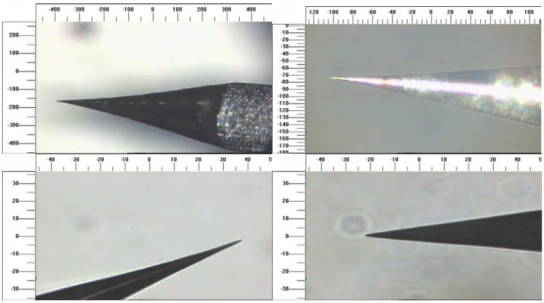
3.7 Four images of tips with good microscopic shape. (Scales are in microns.) The lower right image is a higher magnification image of the tip in the lower left image. The tip in these lower images was not treated with HF(aq) after etching. The deposits on the side of the tip are oxide and hydroxide by-products from the etching process. Higher magnification images of this tip are shown in Figure 3.16 to Figure 3.18. Despite the presence of contaminants on this last tip these show the microscopic consistency of the DC etching process.
81
3.8 Three examples of AC etched tips. They show the variation possible between tips produced by the same AC etching method.
82
3.9 This shows a larger scale image of the same type of tip as in the previous Figure.
82
3.10 A typical DC etched tip. 82
3.11 A more detailed image of the tip shown in the previous Figure. 82 3.12 A second example of a DC etched tip showing the consistency of
the ball shaped end between different tips.
83
3.13 An example of a good DC etched tip that does not have a 'ball-shaped' end.
83
xiv compared to the profile of the tip.
3.15 A higher magnification image of the tip in the previous Figure showing that it does not have a 'ball-shaped' end.
83
3.16 A DC etched tip showing the presence of (hydr)oxide on part of its base.
84
3.17 A higher magnification image of the tip shown in the previous Figure.
84
3.18 The end of the tip shown in the previous Figure. The presence of a DC etched tip can be seen buried underneath the thick (hydr)oxide coating.
85
3.19 A 10.0nm × 9.82nm image of an Au(111) surface recorded with an AC etched tip at 78K, showing a section of herringbone
reconstruction.
85
3.20 A 5nm × 5nm enlarged area of the surface shown in Figure 3.19 showing the individual gold atoms on the surface demonstrating that atomic resolution can be achieved with an AC etched tip. (STM parameters: Ugap = 1V, I = 0.2nA)
86
3.21 A 4.00nm × 4.00nm atomic resolution STM image of an Au(111) surface recorded at 78K with a DC etched tip. (STM parameters:
Ugap = 79.6mV, I = 1.9nA
86
3.22 A 20nm × 20nm image of another Au(111) surface. This was imaged with a DC etched tip at 78K and shows (a modified version of) the herringbone reconstruction. (STM parameters: Ugap
= 99mV, I = 10.5nA
86
4.1 A 400nm × 400nm STM image of an Au sample, which was prepared by annealing with H2/O2 flame without removing it from
the flame. The structure shown in this image is typical of all images recorded from this sample and shows the amalgamation of smaller microcrystalline regions into a larger one indicating that this method of preparation does not produce good Au(111) structure. (STM parameters: Ugap = 0.1V, I = 0.13nA)
93
xv 4.3 A 5µm × 5µm topographical AFM image of an Au sample after
annealing. This image shows the large domains as well as some ‘lumpy’ features both produced by the annealing process.
94
4.4 A 2µm × 2µm phase AFM image of an annealed Au sample, showing an area of Au(111) in the upper part of the image.
95
4.5 A 40nm × 40nm image of an Au sample that had been removed from the flame for 30s as part of the annealing process. No good quality areas of Au(111) were found on this sample. (STM parameters: Ugap = 0.12V, I = 10.5nA)
95
4.6 A room temperature 500nm × 500nm STM image of a sample removed from the flame 7 times whilst it was being annealed. This image shows detailed Au(111) triangle structure. (STM parameters: Ugap = 86mV, I = 1.9nA)
95
4.7 A room temperature 50nm × 50nm STM image of a sample that had been removed from the flame 9 times whilst it was being annealed. The 'noise' of the image is due to it being recorded at room temperature. (STM parameters: Ugap = 97mV, I = 15.4nA)
95
4.8 A 4nm × 4nm 'grainy' room temperature atomic resolution image of the sample that had been removed from the flame 9 times during its annealing process. (STM parameters: Ugap = 95mV, I =
15.4nA)
96
4.9 A section of Au(111) showing a single atom defect. (STM parameters: Ugap = 80mV, I = 1.9nA)
96
4.10 I vs. V and dVdI vs. V curves for Au(111) 97 4.11 STM images of 4nm × 4nm sections of Au(111) terraces recorded
with similar tunnelling parameters. In the left image the changes in the electronic structure is recorded as dark and light areas that give the corrugation a ‘cobblestone’ appearance whereas in the image on the right the light areas are more centred on the lattice positions. The difference in appearance might indicate differences in the tip structure.
xvi diagonal zigzag lines are the carbon chains, the yellow S's are the
sulphur atoms and the horizontal wavy line is the metal surface. 5.2 A 50nm × 50nm STM image of an octanethiol on gold sample,
made using 1mM octanethiol solution showing ‘holes’ in the surface. (STM parameters: Ugap = 426mV, I = 219pA)
107
5.3 Another 50nm × 50nm image of the sample in shown in Figure 4.34, which shows another example of these 'holes' in the thiol layer. (STM parameters: Ugap = 393mV, I = 122pA)
107
5.4 A 200nm × 200nm STM image of an octanethiol on Au sample, made with a 10mM solution of octanethiol. The ‘holes’ can clearly be seen in the gold terrace. (STM parameters: Ugap = 401mV, I =
411pA)
108
5.5 A 100nm × 100nm enlarged section of the sample in Figure 4.36 showing a detailed image of a step edge. The surface density of holes in the 10mM sample appears to be greater than in the 1mM sample. (STM parameters: Ugap = 418mV, I = 210pA)
108
5.6 A 20.0nm × 10.9nm STM image of an octanethiol on Au sample, made with a 100nM octanethiol solution. A ‘hole’ shown in black can clearly be seen towards the top of the image. The ‘holes’ in this sample appear to be due to a change in the packing of the octanethiol molecules. (STM parameters: Ugap = 435mV, I =
504pA)
109
5.7 A 10nm × 10nm STM image of an octanethiol SAM on gold. It was made with a by immersing a gold sample into a 1mM solution of octanethiol overnight in a refrigerator. (STM parameters: Ugap =
491mV, I = 101pA)
109
5.8 A 10nm × 10nm STM image of an octanethiol SAM on gold sample recorded with the same STM but prior to this study and made in a similar way to the sample in Figure 5.7. Note that the spaing between the molecules is similar to that in Figure 5.7. (STM parameters: Ugap = 1V, I = 108pA)
110
5.9
xvii distance between the atomic layers is ≈2Å.
5.10 A stylised representation of octanethiol molecules on a gold surface with some of the molecules at a different angle to the surface than the others showing how such a difference can produce depressions in the surface.
112
5.11 This is the first of two images showing the part of the surface where the octanethiol on Au(111) spectroscopy was recorded. The green and blue dots show the locations where the STS data was recorded presented as the green and blue curves in Figure 5.14. (STM parameters: Ugap = 1.03V, I = 518pA)
114
5.12 This is the second of two images showing the part of the surface where the octanethiol on Au(111) spectroscopy was recorded. The green and black dots show the locations where the STS data recorded presented as the red and black curves in Figure 5.14. (STM parameters: Ugap = 1.03V, I = 518pA)
115
5.13 Black curves: I vs. V and dVdI vs. V STS spectroscopy data from the positions marked by dots shown Figure 5.11 and Figure 5.12. These curves are aggregates of the data at all locations. Red curves: I vs. V and dVdI vs. V STS spectroscopy data from an unexposed Au(111) sample. (Repeated from Figure 4.10)
116
5.14 Showing the similarity in the overall shape of the dVdI vs. V curves recorded using the compensation box and the lock-in amplifier (left) and calculated from the VI vs. V curves (right).
117
5.15 I vs. V and dVdI vs. V curves of STS spectroscopy data from the positions marked by dots shown Figure 5.11 and Figure 5.12, Blue Curves: Depressed areas (blue dots) in Figure 5.11, Green Curves: Non-depressed areas (green dots) in Figure 5.11, Black Curves: Raised areas (black dots) in Figure 5.12, Red Curves: Non-raised areas (green dots) in Figure 5.12
119
5.16 A 200nm × 200nm section of an Au(111) surface covered with dimethyl disulphide.
xviii Figure.
5.18 A 50nm × 50nm image of a section of Au(111) for comparison with the previous Figure. (STM Parameters: Ugap = 80mV, I =
2.2nA)
124
5.19 A 20nm × 20nm section of Au(111) surface showing some features in the Au surface and a line of adsorbed molecules.
126
5.20 A 10nm × 10nm section of another part of the surface showing the Au atoms with some thiol molecules adsorbed on the surface. Note the relative orientations of the molecules to one another.
126
5.21 A 5nm × 5nm section of Au(111) surface showing more clearly five of the molecules in the previous Figure.
126
5.22 An image of the surface slightly displaced from that in the previous Figure.
126
5.23 Showing two possible orientations of DMDS molecules on the Au(111) surface.
127
5.24 Showing two methyl sulphide groups attached to the Au(111) surface. Note that here the S C bonds are perpendicular with the surface.
128
5.25 Showing a single methyl sulphide unit attached to the Au(111) surface, with the angle of the S C bond approximately 50º to the surface normal as suggested by Akinaga, Nakajima, and Hirao.
128
5.26 A 200nm × 200nm image of an methanethiolate coated Au(111) sample.
129
5.27 A differentiated version of the image in Figure 5.26. This is similar to Figure 4 from Dishner et al.[12] suggesting that the surface is coated with methanethiolate as expected.[13]
129
5.28 Showing the area of the surface where the topographically varying scanning tunnelling spectroscopy was recorded. The spectra were recorded to attempt to determine the nature of the feature on the left hand side in the image. (STM Parameters: Ugap = 200mV, I =
150pA)
131
xix An I vs. V curve and a dV vs. V plot of the spectroscopy data
collected from the Au sample coated with a methylthiolate SAM. 5.31 I vs. V curves and dVdI vs. V plots of the spectroscopy data collected
from an uncoated Au sample. The red and blue curves correspond to two sets of measurements made with the same tip on the same surface.
134
5.32 A section of the 2 2 dV I
d vs. V curve calculated from the dV
dI vs. V
curve overlaid with the dVdI vs. V curve. Due to the method of calculation there is a slight offset between the two curves.
135
6.1 A plot showing the frequency and voltage dependence of the LDSTM response represented on the vertical axis as the magnitude output of the lock-in amplifier. The horizontal axis shows the modulation frequency of the AOM. Note the logarithmic scale on both axes. Experimental conditions: I = 2nA, τ = 1s, feedback loop gain = 3%, laser power = 10mW and λ = 2974cm-1
= 3.362µm.
152
6.2 Identical to the previous Figure but with the addition of the black curve displaying data from an experiment in which the tunnelling current was varied by a modulated applied voltage rather than a modulated laser beam. This shows the frequency response of the STM electronics and allows the LDSTM data to be seen in context of the characteristics of the STM.
154
6.3 This shows the results of LDSTM experiments recording the effect of the tunnelling current on R. They were recorded with experimental conditions of: Methylthiolate on gold sample. Tunnelling voltage: 0.5V, τ = 1s, feedback loop gain = 3%, λ = 2974cm-1 = 3.362µm, laser power = 10mW.
155
6.4 This shows the same data as in the previous Figure but with the lock-in magnitude output as a function of the modulation frequency. Experimental conditions as described in the caption for the previous Figure.
xx samples coated and uncoated with methylthiolate. Other
experimental conditions: Tunnelling voltage = 0.5V, feedback loop gain = 3%, λ = 3.362µm = 2974cm-1, τ = 1s, I = 1nA, laser power = 10mW. The same tip was used for both samples.
6.6 Showing the LDSTM response to the wavelength of the laser. Samples: coated and uncoated Modulation frequency: ■ = 3.23
kHz,
▲
= 4.6 kHz. Other experimental conditions: τ = 1s, I = 1nA, feedback loop gain = 3%, laser power = 10mW. The black data points show additional data for laser wavelengths between 3.16µm and 3.36µm. These were generated by varying the temperature of the 29.75µm grating from 100ºC to 190ºC.
158
6.7 Showing how the change in gradient at 0.42V in the methylthiolate
dV
dI vs. V spectrum occurs at a similar energy to the increase in modulation of the tunnelling current of the coated sample. The insert is a copy of Figure 5.27. The main figure shows a section of this dVdI vs. V curve from 0.25V to 0.5V (black curve, right axis) overlaid with data from Figure 5.27 (red and blue data, left axis).
1
1
Chapter 1
Introduction
1 Chapter 1 Introduction ... 1
2
1.1 Chapter Introduction
The pursuit of knowledge about the world around us is relentless and our drive to understanding the building blocks of the universe results in large sums of money being spent on multi-national ‘big science’ projects such as the new Large Hadron Collider at CERN[1]. However despite the discoveries made of these exotic subatomic particles, it is not possible to use these to derive all the characteristics about the atoms and molecules that form the basis of the world that we experience day to day. There are still many things of importance to learn from the latter. Until relatively recently almost all of the research in this area focussed upon studying macroscopic quantities of these atoms or molecules. In biological situations particularly, the situation is made more complicated by the necessity to study mixtures as provided by nature with only limited ways of controlling the molecular species in a system under investigation. There is great value in being able to study a single molecule (whether it is large or small) to cut through the averaging that takes place within a macroscopic sample.
For hundreds of years microscopy has been used as a way of studying our world. The samples examined have become smaller and smaller as the optical technology has improved. However the resolution of this technique is fundamentally limited by diffraction. Confocal microscopy can, to a limited degree overcome this problem and combined with partial selective tracing of biological molecules of interest can even track the movement of individual molecules. More recently a range of scanning probe microscopy (SPM) techniques has been developed, the first of which, scanning tunnelling microscopy (STM), still has the highest spatial resolution of a few Å. This is able to manipulate and record single molecules. With the advent of SPM the need arose to be able to manipulate systems on the nanoscale in a controlled way to provide suitable test samples (examples of which are described below) that could be studied with these new techniques.
3 Photoelectric Spectroscopy) is limited. Although LEED can accurately determine the dimensions of a repeating structure, it is not able as a consequence of the diffraction process to record details of individual molecules or surface defects. With XPS the situation is better. It is possible to conduct imaging with XPS but at best the resolution is limited to ≈120nm.[5]
Figure 1.1: An example of a self-assembled monolayer of methanethiolate on gold. This cartoon is based upon a unit cell by De Renzi et al.[6] used for calculating the postions of the
thiolate species on the surface.
With the advent of SPM and STM in particular the structure of such surfaces could be investigated at a molecular scale provided that suitable substrates are used. This gave an opportunity to start to work with individual molecules and atoms. STM provides an opportunity to find out how the individual properties of the constituent atoms and molecules combine together to give the macroscopic measurement. Although STM can image individual molecules, often it is difficult to resolve their substructure. This makes it difficult to identify a molecule found on a surface, without knowing what was put into the ultra high vacuum (UHV) chamber in the first place, particularly when the size of an atom or molecule is determined by its total electron density, rather than the electron density at the energy of the tunnelling electrons. The latter being the characteristic that the STM measures.
4 molecules partially because of the selection rules that restrict its use to certain vibrational transitions[8-10]. Conventional spectroscopic techniques are better able to record information to distinguish between different species, but even when incorporated with a near field technique (SNOM) the resolution cannot approach that of an STM. Here the sharp (metallic) tip enhances the electric field in its immediate proximity and a small area of the surface underneath the tip modifies the scattered radiation from this tip. The microscopic shape of the tip limits the size of this area and consequently the spatial resolution obtained. This interaction of radiation between the tip and the sample is such that it is the near field radiation from near this surface that the tip is able to scatter into the far field whilst maintaining the spatial resolution of the near field information. Alternatively, illuminating an STM tip with laser radiation and detecting its effect, as a modulation of the tunnelling current should yield higher spatial resolution because the resolution is determined by the resolution of the STM.
5
1.2 Overview of the Work
The high spatial resolution available with an STM and the chemical information available from infrared spectroscopy leads to a description of the aim of this project: to use an Optical Parametric Oscillator (OPO) as a tuneable infrared laser source coupled with an STM to probe the response of samples to the infrared radiation with the spatial resolution of the STM. This project works towards a technique for identifying singular molecular species and studying their interaction with the surface. Typical samples are expected to be metal substrates partially or completely covered with molecules with vibrational modes accessible by the OPO.
1.3 Outline of Thesis
1.3.1 Chapter 1: Introduction
This chapter introduces the aim of the project in the context of a brief summary of work conducted previously and lists outlines of the chapters in this thesis.
1.3.2 Chapter 2: Technologies and Techniques Used
Conducting experiments at low temperatures improves the quality of the images and STM spectroscopy recorded[23] due to the reduction of the atoms’ thermal motion and the narrowing of the vibrational modes. As a consequence it was decided to use a low temperature STM (LTSTM) to take advantage of this. §2.1 provides an overview of STM and describes details of the particular LTSTM used in this study.
6 Self-assembled monolayers (SAMs) prepared on gold were used as the basis for the samples used, mostly as a consequence of the restricted types of substrate available for use with this STM. For an overview of SAMs and their manufacture see §2.4.
Coupling a laser with an STM forms the key experiment conducted as part of this work. §2.5 provides a history of this type of experiment and describes a theoretical basis for its use.
1.3.3 Chapter 3: Scanning Tunnelling Microscopy Tips
The STM tip is a critical component of the STM. Manufacturing tips with reproducible quality is not easy but it is important that this is achieved. Chapter 3 describes the procedures developed for making the tips used in the STM. Optical and electron microscope images of these tips are used to show the effectiveness of the tip etching methods. STM images recorded with these tips are included to illustrate their quality. Conclusions are drawn from these various images and suggestions are made for potential future improvements.
1.3.4 Chapter 4: Au(111) Samples
7
1.3.5 Chapter 5: Thiol Self-Assembled Monolayers
Although the reactivity of gold is quite low it will react readily with thiol molecules (containing sulphur atoms) either as an –S-H group or as a dithiol (-S-S-) group. §5.2 describes the preparation of self-assembled monolayers of octanethiol onto gold substrates and their subsequent imaging with the STM. This section also includes details of scanning tunnelling spectroscopy experiments conducted on the octanethiolate samples. §5.3 describes experiments conducted with samples of dimethyl disulphide deposited onto Au(111) including details of the method used to make these samples. The experiments used include STM imaging and STM spectroscopy. The chapter concludes with discussions of the results of the experiments conducted and makes suggestions for future experiments.
1.3.6 Chapter 6: Laser Driven Scanning Tunnelling Microscopy Experiments
A key part of the area of interest of this thesis is the nature of the interaction between the beam from an OPO and the tunnelling junction in an STM. This chapter describes the details of the experiments that combine the laser with the STM. A series of subsections highlight a range of key variables and the experiments used to investigate them. The chapter concludes with a discussion of the results collected from these experiments and makes suggestions for further work.
1.3.7 Conclusions
8
1.4 References
1. Rogers, P., To the LHC and beyond. Physics World, 2004. 17(9): p. 64. 2. Emmons, H., Trans. Am. Inst. Chem. Eng., 1939. 35: p. 109-.
3. Schmidt, E., W. Schurig, W. Sellschopp, Tech. Mech. Thermodyn., 1930.
1: p. 53-.
4. Nagle, W.M., T. B. Drew, Trans. Am. Inst. Chem. Eng., 1933. 30: p. 217-. 5. Escher, M., et al., NanoESCA: imaging UPS and XPS with high energy
resolution. Journal of Electron Spectroscopy and Related Phenomena,
2005. 144-147: p. 1179-1182.
6. De Renzi, V., et al., Ordered (3 x 4) high-density phase of methylthiolate
on Au(111). Journal of Physical Chemistry B, 2004. 108(1): p. 16-20.
7. Ho, W., Single-molecule chemistry. The Journal of Chemical Physics, 2002. 117(24): p. 11033-11061.
8. Mingo, N., Calculation of the Inelastic Scanning Tunneling Image of
Acetylene on Cu(100). Phys. Rev. Letters, 2000. 84(16): p. 3694-3697.
9. Lorente, N. and M. Persson, Theory of single molecule vibrational
spectroscopy and microscopy. Physical Review Letters, 2000. 85(14): p.
2997-3000.
10. Lorente, N., et al., Symmetry Selection Rules for Vibrationally Inelastic
Tunneling. Physical Review Letters, 2001. 86(12): p. 2593-2596.
11. Grafström, S., Photoassisted scanning tunneling microscopy. J. Appl. Phys., 2002. 91(4): p. 1717-1753.
12. Kroo, N., et al., Decay Length of Surface-Plasmons Determined with a
Tunneling Microscope. Europhysics Letters, 1991. 15(3): p. 289-293.
13. Grafström, S., et al., Thermal expansion of scanning tunneling microscopy
tips under laser illumination. Journal of Applied Physics, 1998. 83(7): p.
3453-3460.
14. Krieger, W., et al., Generation of Microwave-Radiation in the Tunneling
Junction of a Scanning Tunneling Microscope. Physical Review B, 1990.
41(14): p. 10229-10232.
15. Grafström, S., Analysis and compensation of thermal effects in
laser-assisted scanning tunneling microscopy. Journal of Vacuum Science &
9 16. Grafström, S., et al., Investigation of laser-induced effects in molecular
layers by scanning tunneling microscopy. Applied Physics A-Materials
Science & Processing, 1998. 66: p. S1237-S1240.
17. Amer, N.M., A. Skumanich, and D. Ripple, Photothermal modulation of
the gap distance in scanning tunneling microscopy. Applied Physics
Letters, 1986. 49(3): p. 137-139.
18. Specht, M., et al., Scanning Plasmon near-Field Microscope. Physical Review Letters, 1992. 68(4): p. 476-479.
19. Gutjahr-Loser, T., et al., Ferrimagnetic resonance excitation by light-wave
mixing in a scanning tunneling microscope. Journal of Applied Physics,
1999. 86(11): p. 6331-6334.
20. Landi, S.M. and O.E. Martinez, Quenching the thermal contribution in
laser assisted scanning tunneling microscopy. Journal of Applied Physics,
2000. 88(8): p. 4840-4844.
21. Moltgen, H. and K. Kleinermanns, Resonance enhanced scanning
tunneling (REST) spectroscopy of molecular aggregates on graphite.
Physical Chemistry Chemical Physics, 2003. 5(12): p. 2643-2647.
22. Smith, D.A. and R.W. Owens, Laser-assisted scanning tunnelling
microscope detection of a molecular adsorbate. Applied Physics Letters,
2000. 76(25): p. 3825-3827.
23. Ferris, J.H., et al., Design, operation, and housing of an ultrastable, low
temperature, ultrahigh vacuum scanning tunneling microscope. Review of
10
2
Chapter 2
Techniques and Technologies Used
2 Chapter 2 Techniques and Technologies Used ... 10
11
2.1 Chapter Introduction
This chapter describes the equipment and the experimental techniques used to conduct the experiments. It is comprised of four sections. It starts by introducing the technique of scanning tunnelling microscopy and describes details of the specific STM used to collect the data included in this work. A sub-section is included describing how STM spectroscopy can be conducted on samples by varying the tunnelling conditions. Section 2.3 introduces the optical parametric oscillator as the laser source used to irradiate the sample during the laser driven scanning tunnelling microscopy (LDSTM) experiments. Section 2.4 describes self-assembled monolayers (SAMs) and why they are a useful system to study with LDSTM. The chapter concludes with a look at LDSTM itself. An overview and history of part of the field is discussed highlighting how the technique is an improvement over conventional spectroscopy or STM techniques alone.
2.2 Scanning Tunnelling Microscopy
2.2.1 A Brief History
12 tunnelling[4] can also be applied to STM. However, since with an STM the current ideally only tunnels though one atom the signal-to-noise ratio will be significantly worse. It is only in the last few years that STM technology has caught up and been used to do similar experiments on a single molecular scale[5]. In the years that followed, other groups started work with STM using any conductive sample that could be prepared with a regular structure e.g. graphite, III-V semiconductors, and metals prepared with (111), (110) or (100) surfaces. Although well-ordered surfaces are easier to study, many surface chemical and physical processes take place at the defects that exist on the surfaces. STM provided a way of studying these defects individually providing greater insight into such processes.
As the features of simple surfaces had been reasonably well understood, the attention of those using STM moved to surfaces that were more complicated, typically involving a metal substrate with other atoms or molecules on its surface[6, 7]. These additional atoms on the surface could either be scattered sparingly or as a monolayer or as a multilayer. Some of IBM’s most famous work required a low concentration of atoms on the metal surface.[8] Initially these experiments were designed to demonstrate successes in actively positioning atoms on a surface.[8] Later the electron standing waves produced by a specific arrangement of atoms became of interest.[7, 9-11] Currently the ‘cutting edge’ of the field includes work based around single molecule inelastic tunnelling experiments exploring the possibilities of initiating reactions with one molecule of each reagent[12].
As the progress of STM experiments proceeded over the years, ideas for the theoretical understanding of STM were developed in parallel. Initially these were derived from tunnelling electron flow between the two metals in a metal-oxide-metal ‘sandwich’.[13] By the 1980’s they had become more sophisticated, adding effects due to the different spatial arrangements between metal-oxide-metal and STM systems.[14]. More recently efforts have focussed on the role of the character of the tip in influencing the STM images[15-17].
13
2.2.2 An Overview of STM
In STM a potential difference is applied between a conducting surface and a very fine point (tip) a few Ångstroms just above the surface (Figure 2.1). The voltage applied is enough to enable electrons to tunnel across the vacuum gap between the surface and the tip (or vice versa). The particular polarity and magnitude of the voltage for any given experiment will depend upon the sample used and what is of particular interest in that sample. The number of electrons that tunnel from the surface to the tip (or vice versa) is exponentially dependent upon the distance between the surface and the tip[14]; i.e. the further away the tip is from the surface the lower the current will be. The tip is raster scanned across a section of sample surface and the current between the surface and the tip is measured continuously (see Figure 2.1). This tunnelling current is dependent on the electronic properties of the tip and sample and approximately exponentially dependent upon the distance between the tip and the sample.
Piezoelectric Stack
Tip
Piezoelectric Controller
V I
Surface
Figure 2.1: Schematic of the tunnelling set-up. A very sharp metal tip is positioned very close
to the surface and a voltage is applied between the two, as the tip is raster scanned across the
surface whilst the current is measured.
14 topography of the surface without the tip colliding into the surface. The tip is moved in three dimensions with a stack of piezoelectric material. Applying a voltage across the stack in an appropriate direction moves one end of this material, onto which the tip is attached. The distance that the piezoelectric stack has to move to keep the current constant is recorded and plotted to produce a topographical map of the surface.
STM experiments can be carried out under a wide range of different conditions: air[18], liquid (both polar[19] and non-polar[20]) and ultra-high vacuum (UHV)[18]. Images recorded from experiments conducted in air tend to be of poorer quality than those conducted in UHV due to species in the atmosphere contaminating the sample but it is much more convenient to work in air than in UHV so conducting experiments in air can still be useful. For STM experiments in liquids the issue of contamination is more acute due to the surface being continuously in contact with the species present in the liquid used. This requires that the liquid does not contain any undesirable species that would adsorb on the surface for an appreciable length of time. STM experiments are only usually conducted in liquids in order to investigate the interaction of the sample with the constituents of the liquid.[21] As a consequence of the reduced risk of contamination, experiments run in UHV produce images with better quality, which is why the experiments documented in this report took place in UHV. In addition, it is more difficult to image the atoms in a surface at room temperature since the STM is sensitive enough to measure their thermal motion. Consequently, much of the data included in this report has been recorded with the apparatus cooled to 77K (with N2(l)) and some of it was
recorded with the apparatus cooled to ≈5K (with He(l)).
2.2.3 A Theoretical Approach
15
2.2.3.1
The Rectangular Barrier
At the simplest level, the tunnelling process can be described in one dimension with a rectangular shaped potential barrier. The energy of the wavefunction of the tunnelling electron is kept constant. This simple case can be described best in a time independent manner. For a simple rectangular barrier, there are three regions of interest that have the following time-independent Schrödinger equations and associated wavefunctions for an electron of mass m and energy E[22] (see Figure 2.2),:
x < 0 0 ≤ x ≤ L V0 x > L
Figure 2.2: Illustrating the simple case of tunnelling through a rectangular shaped barrier.
The electron is considered to travel from the left to the right along the x axis. Between x = 0
and x = L there is a potential barrier with a height of energy V0.
The probability of transmission for the electron is calculated by matching the wavefunctions and their first derivatives at the interfaces between these three regions.
1. Left hand side of barrier (x < 0):
Equation 2.1 and Equation 2.2 show the Time Independent Schrödinger Equation (TISE) and the electron wavefunction for this region respectively.
1 2
1 2 2
2 = Ψ
Ψ −
E
dx
d
m
h
Equation 2.1
) ( )
( 1
t kx i t
kx i
Ae e −ω + − +ω
=
Ψ where 2 2 2
h
mE
16 The two parts of Ψ1 show that it has two components, one incident to and the
other reflected from the barrier. The A in the second, reflected part enables these two components to have different magnitudes.
2. In the barrier (0 ≤ x ≤ L):
Equation 2.3 and Equation 2.4 show the TISE and the electron wavefunction for this region respectively. Note the addition of the terms containing V0
(barrier height or workfunction) due to the presence of the wavefunction in the potential barrier.
2 2 0 2 2 2 2
2 + Ψ = Ψ
Ψ − E V dx d m h Equation 2.3
where 2 2 ( 02 )
'
h
E V m
k = − Equation 2.4
Also the exponential parts of Equation 2.4 are real resulting in the exponential shape of the wavefunction inside the barrier compared to the periodic shape outside the barrier.
3. Right hand side of the barrier (x > L):
Equation 2.5 (the TISE for this region) has a similar form to Equation 2.1 due to the absence of the potential for x > L. Equation 2.6, the expression for Ψ3
only contains one term due to the electrons in this region only propagating away from the barrier. Note the x – L term used to describe the position of the electron to displace the origin of the wavefunction from x = 0 to x = L.
3 2
3 2 2
2 = Ψ
Ψ − E dx d m h Equation 2.5 ) ) ( ( 3 t L x k i
De − −ω
=
Ψ where 2 2 2
h
mE
17 The proportion of electrons that tunnel through the barrier is given by the transmission coefficient T, given by:
i t j j
T = Equation 2.7
where jt is the transmitted current density and ji is the incident current density. In
the one dimensional case current density, j (sometimes referred to as particle flux) is given by[23]:
Ψ Ψ − Ψ Ψ − = dx d dx d m i j * * 2 h Equation 2.8
For jt, Ψ = Ψ3:
Ψ Ψ − Ψ Ψ − = ∗ ∗ dx d dx d m i
jt 3
3 3 3 2 h Equation 2.9 More explicitly: ( ) ( )
(
(( ) ))
(( ) )(
( ( ) ))
− −= −ikx−L− t ikx−L− L ikx−L− L −ikx−L− L
t De dx d De De dx d De m i
j ω ω ω ω
2
h
Equation 2.10
This simplifies to:
2 D m k jt h
= Equation 2.11
For ji, Ψ equals the first term in Ψ1:
(
)
(
)
− − = −( − ) ( − ) ( − ) −( − ) 2 t kx i t kx i t kx i t kx i i e dx d e e dx d e m ij h ω ω ω ω Equation 2.12
This simplifies to:
m k ji
h
= Equation 2.13
Therefore:
18 The wavefunctions Ψ1, Ψ2, and Ψ3 have boundary conditions that require the
wavefunctions and their first derivatives to be matched at the interfaces between these three regions. Satisfying these boundary conditions for Equation 2.1 to Equation 2.6 leads to four simultaneous equations for A, B, C, & D.
1 + A = B + C Equation 2.15
ik – ikA = k'C – k'B Equation 2.16
Be-k'L + Cek'L = D Equation 2.17
k'Cek'L – k'Be-k'L = ikD Equation 2.18
Equation 2.15 to Equation 2.18 can be solved to yield D and consequently |D|2. To do this, Equation 2.15 and Equation 2.16 are combined to eliminate A and rearranged: ik k ik k B ik C + − + = ' ) ' ( 2 Equation 2.19
Inserting Equation 2.19 into Equation 2.17 and rearranging for B yields:
) ' sinh( 2 ) ' cosh( ' 2 2 ) ' ( ' L k ik L k k ike D ik k B L k − − +
= Equation 2.20
Inserting Equation 2.19 into Equation 2.18 and rearranging for B yields:
) ' cosh( ' 2 ) ' sinh( ' 2 ' 2 ) ' ( 2 ' 2 L k k ik L k k ke ik D k k ik B L k − − −
= Equation 2.21
Setting Equation 2.20 equal to Equation 2.21 and rearranging for D gives:
) ' cosh( ' 2 ) ' sinh( ) ' ( ' 2 2 2 L k k ik L k k k k ik D − +
19 Consequently T is given by:
) ' ( cosh ' 4 ) ' ( sinh ) ' ( ' 4 2 2 2 2 2 2 2 2 2 2 L k k k L k k k k k D T + + =
= Equation 2.23
For the scenarios described in this thesis the de Broglie wavelength of the tunnelling electrons is less than the barrier width. In this regime Equation 2.23 becomes:
L
E
V
m
E
V
E
V
E
V
E
e
T
2
(
)
)
(
4
)
(
4
2 00 2
0
0
−
−
−
+
−
≈
hEquation 2.24
Despite the simplicity of this model some important points can be drawn from it. In this approximate expression for T the exponential part dominates. The exponential dependence of T on the barrier width L is what enables an STM to resolve the variation of the electron density on a surface with such high spatial resolution. T is similarly exponentially dependent upon the square root of the effective barrier height V0 −E. The exponential dependence of the probability of tunnelling upon the effective barrier height is also true for barriers with a more general shape. This is shown in §2.2.3.3 which describes the Wentzel, Kramers and Brillouin (WKB) model.[24]
2.2.3.2
The Barrier Height (Workfunction)
It is important to realise that a spatial variation in the barrier height (V0) will affect
20 measurement of the barrier height (workfunction) by making use of a simplified version of Equation 2.24. If the workfunction (V0) is significantly larger than E
then the exponential component of this expression can be considered to be independent of the electron energy and the pre-exponential factor simplifies to
0
4VE implying that the tunnelling probability (and consequently the tunnelling current) is linearly dependent upon the electron energy. At a fixed value of the electron energy E this can be expressed in the following form:
L mV
Ee
I
∝
−2h 2 0Equation 2.25
Despite the simplicity of such a model it does provide a good approximation and experimentally the tunnelling current can in many cases be found to be linearly dependent upon the applied voltage. If the approximation of regarding the exponential part as independent of E is assumed to be valid then this provides a simple way of measuring the workfunction. At a fixed value of E, Equation 2.25 can be simplified further to:
L m
e
I
∝
−2h 2 ϕEquation 2.26
where φ is an effective workfunction (barrier height). By recording the tunnelling
current (I) for different values of the tip sample separation (L), φ can be calculated
from gradient of a plot of lnI vs. L. As described above this model is intended to be used when V0 is much larger than E. When V0 is only slightly larger than E a
more complex expression should be used[25]:
(
)
[
(
)
]
(
)
[
(
0 2)
]
2 2 0 2 2 2 0 2 2 0 E L EL mV
E V
m
E
e
V
e
V
I
∝
−
− h −−
+
− h +Equation 2.27
21
2.2.3.3
The WKB Model
This model is more sophisticated than the rectangular barrier case in that it considers a barrier with an arbitrary shape (see Figure 2.3). This treatment allows the shape of the potential barrier to be included in order to more accurately model the tunnelling process and provides a better estimate of the pre-exponential factor. However, this flexibility comes at a price and this is that the model does not work when the energy of the electrons is close to that of the potential barrier. This limitation can be overcome by restricting the barrier to one with a linear shape, but of course this removes the flexibility of working with an arbitrarily shaped barrier (see Figure 2.4).
Figure 2.3 (Above): Showing a wavefunction tunnelling through a barrier of arbitrary shape.
This scenario can be described with the WKB model but only if the electron energy is not
near the height of the barrier.
Figure 2.4 (Above): The WKB approximation can be made to work when the electron energy
is close to the barrier height if a linear barrier is used. Removing the restriction on the
electron energy comes at a cost of only being able to use a barrier with a linear shape.
22
) ( ) (x T x iS
e
+=
ψ
Equation 2.28Here just the spatially dependent part is included for clarity. The wavefunction is a combination of periodic and exponential components.
Firstly take the Time Independent Schrödinger Equation (TISE):
ψ ψ ψ E V dx d
m + =
− 2 2 2 2 h Equation 2.29
and rearrange it:
(
)
ψψ ψ 2 2 2 h V E m d
d − −
= Equation 2.30
Insert the wavefunction ψ:
(
)
ψψ 2 2 2 2 2 2 2 2 2 h V E m dx dT dx dT dx dS i dx dS dx T d dx S d
i = − −
+ + −
+ Equation 2.31
Cancelling ψ and writing the real and imaginary parts separately yields:
0 2 2 2 2 2 = + + + − k dx dT dx T d dx dS Equation 2.32 and: 0 2 2 2 = + dx dT dx dS dx S d Equation 2.33 where:
( )
(
)
2 2 2 h x V E mk = − Equation 2.34
Let us consider cases where the oscillation of the wave function is very rapid compared to any non-periodic changes in its amplitude, i.e. when the wavelength,
λ
23 dx dS dx T d << 2 2 and dx dS dx dT <<
. These can be used to approximate Equation 2.32 to
2 2 k dx dS =
, leading to:
k dx dS
±
= . Equation 2.35
Integrating Equation 2.35 gives:
( )
x =±∫
kdxS Equation 2.36
and differentiating Equation 2.35 gives:
dx dk dx
S d =±
2 2
Equation 2.37
Inserting Equation 2.35 and Equation 2.37 into Equation 2.33 and rearranging gives:
dx dk dx
dT k =−
2 Equation 2.38
Integrating Equation 2.38 gives:
T = -½ln k + c Equation 2.39 (c = constant of integration) Rearranging:
k A
eT(x) = Equation 2.40