promoting access to White Rose research papers
White Rose Research Online
[email protected]
Universities of Leeds, Sheffield and York
http://eprints.whiterose.ac.uk/
This is a copy of the final published version of a paper published via gold open access
in
Journal of Materials Chemistry C
.
This open access article is distributed under the terms of the Creative Commons
Attribution Licence (
http://creativecommons.org/licenses/by/3.0
), which permits
unrestricted use, distribution, and reproduction in any medium, provided the
original work is properly cited.
White Rose Research Online URL for this paper:
http://eprints.whiterose.ac.uk/79517
Published paper
All-polymer
fi
eld-e
ff
ect transistors using a brush gate
dielectric
†
Ana B. Rodr´ıguez,aMichael R. Tomlinson,aSaghar Khodabakhsh,bJui-Fen Chang,‡c Fabrice Cousin,dDieter Lott,eHenning Sirringhaus,cWilhelm T. S. Huck,§b
Anthony M. Higginsfand Mark Geoghegan*a
Interfaces between a poly(3-hexylthiophene) [P3HT] and an end-grafted (brush) layer of poly(methyl methacrylate) [PMMA] are shown using neutron reflectometry to be dependent on heat treatment. Annealing the samples allows part of the brush layer to cross into the P3HT layer creating a very asymmetric interface. We suggest that the P3HT rearrangement occurs, creating space for movement of the brush into the film. This interpenetration was observed with two different molecular weight (17.5 and 28 kg mol1) P3HT films. Output characteristics of devices made from P3HT layers on PMMA
brushes show that different amounts of heat treatment do not significantly change the device performance. Saturated hole mobilities are dependent on heat treatment, with devices made from a smaller molecular weight P3HT (22 kg mol1) demonstrating larger mobilities than devices created
using 48 kg mol1P3HT, but only after heat treatment.
1
Introduction
All-polymereld-effect transistors (FETs) have been developed for a number of years due to their impressive processability and to further improve development ofexible devices. The lack of a need for expensive fabrication facilities is a major advantage, but ease of preparation of devices is also of some importance.1,2
A facile means of creating all-polymer devices is to spin-coat the active layer onto the gate dielectric, but each polymer layer requires a different solvent, with a solubility orthogonal to that of the preceding layer to prevent dissolution of the device during preparation.3,4Such a limitation has restricted the use of
solvent castlms for all-polymer devices.
Optimal transistor performance requires layers with complete integrity as well as interfaces free of traps. This is particularly true in the case of the dielectric layer, because leakage and short-circuiting are caused by imperfections and pinhole defects. Although making thicker dielectric layers is more likely to provide layer integrity, longer channel lengths, L are required, since Lmin f t3, where t3 is the
thickness of the gate dielectric and Lmin is the minimum
channel length appropriate for that dielectric thickness. The shorter the channel, the more difficult it becomes to control (“pinch off”) theow of carriers in the semiconductor, and a thinner gate layer is required. It is important to have the gate layer as thin as possible in order that a smaller gate voltage be required to maintain the required charge density at the interface.5,6
The use of surface-graed polymers conveys inherent advantages in the creation of polymer transistors.7,8To graa
polymer from the surfacerst requires an initiator layer, which self-assembles on the surface. A gold electrode presents an ideal surface for thiol-terminated initiators. The surface must be imperfection free to support complete coverage by the initiator. During synthesis, the polymer is grownin situfrom the surface allowing a high graing density to be achieved. The resultant close packing of the chain ends results in a stretched polymer conformation, which gives rise to the descriptive term“polymer brush”. Because the brush has been chemically graed onto the substrate, the deposition of the next layer by solvent casting will not remove the graed polymer. This does not mean that orthogonal solvents are no longer preferable, but it does miti-gate the problem of layer dissolution and possibly also of poor
aDepartment of Physics and Astronomy, University of Sheffield, Sheffield S3 7RH, UK. E-mail: mark.geoghegan@sheffield.ac.uk
bMelville Laboratory for Polymer Synthesis, Department of Chemistry, University of Cambridge, Lenseld Road, Cambridge, CB2 1EW, UK
cDepartment of Physics, Cavendish Laboratory, J. J. Thomson Avenue, Cambridge CB3 0HE, UK
dLaboratoire L´eon Brillouin, CEA-CNRS UMR12, CE-Saclay, F-91191 Gif-sur-Yvette C´edex, France
e
Institute for Materials Research, GKSS-Forschungszentrum Geesthacht, D-21502 Geesthacht, Germany
fCollege of Engineering, Swansea University, Swansea SA2 8PP, UK
†Electronic supplementary information (ESI) available: Contains the output characteristics for all devices measured and tabulated device data. See DOI: 10.1039/c3tc31076k
‡Present address: Department of Optics and Photonics, National Central University, Jhongli, Taoyuan 32001, Taiwan.
§ Present address: Institute for Molecules and Materials, Radboud University Nijmegen, Nijmegen 6525, Netherlands.
Cite this:J. Mater. Chem. C, 2013,1, 7736
Received 5th June 2013 Accepted 9th September 2013
DOI: 10.1039/c3tc31076k
www.rsc.org/MaterialsC
Materials Chemistry C
PAPER
Open Access Article. Published on 10 September 2013. Downloaded on 24/06/2014 14:45:31.
This article is licensed under a
Creative Commons Attribution 3.0 Unported Licence.
View Article Online
device performance due to mixing or roughness at the interface between the dielectric and active layers.4,9The dielectric layer is
therefore more chemically robust when graed from a surface. It can be expected for a polymer brush dielectric that intimate mixing at the interface with the active layer would be sup-pressed due to the entropic penalty incurred by the further stretching of the brush molecules and signicant interpene-tration into the active layer. The use of brush gate layers has been demonstrated previously for different systems.7,8In our
earlier work,7we demonstrated the use of atom transfer radical
polymerization (ATRP) as a means to grow poly(methyl meth-acrylate) (PMMA) gate dielectric layers from a gold surface. Here we develop the theme and discuss the performance of devices made of a poly(3-hexylthiophene) (P3HT) active layer on PMMA brush layers for two different P3HT molecular masses.
2
Materials and methods
2.1 Brush synthesis
The PMMA brush layers were prepared by a “graing-from” ATRP synthesis. Silicon wafers of 5 mm thickness and 5 cm diameter were employed for the neutron reectometry experi-ments. For the fabrication of the electronic devices, a sample geometry of SiO2/PMMA/P3HT/gold was used. The gate
dielec-tric brush was grown using ATRP on 0.5 cm2thin silicon wafers
for the electronic devices. The substrates were cleaned by three solvent sonication (water, acetone, and methanol) followed by oxygen plasma cleaning. The substrates were then immersed overnight in a dilute anhydrous toluene solution of (11-(2-bromo-2-methyl)propionyloxy) undecyltrichlorosilane (the initiator for surface ATRP) held at10C, which allowed a self-assembled monolayer of the initiator to be formed.
The PMMA brushes were grown for up to 30 h in a solution containing 2.7 mL MMA, 0.051 g CuCl, 1 mg CuCl2, and 0.173 g
2,20-bipyridine dissolved in a mixture of 2.7 mL methanol and 0.55 mL deionized water. The time allowed for the brushes to grow affected theirnal thickness (a maximum of 70 nm) but not the graing density. During the growth process, the sample was kept at room temperature for different times, depending on the desired thickness for the brush. Polymer brushes were cleaned by light rinsing with acetone and propan-2-ol, aer a brief sonication in water.
For the neutron reectivity samples, deuterated monomer was used in the brush synthesis. The resulting (dPMMA) brushes have a signicantly larger scattering length density than the semi-conducting P3HT layers above them, enabling the interfacial structure to be assessed. P3HT was deposited by spin coating from chloroform (which is also a good solvent for PMMA), with two different molecular weights used: 17.5 kg mol1(P3HT17; with regio-regularity >90% as stated by the supplier, Sigma Aldrich) and 28 kg mol1(P3HT28; with stated regio-regularity of between 95 and 98% from American Dye Source).
2.2 Neutron reectometry
Neutron reectometry measurements were made using the time-of-ight EROS reectometer of the Orph´ee reactor at the
Laboratoire L´eon Brillouin, or the monochromatic NERO re ec-tometer at the Geesthacht reactor. Neutrons are scattered by atomic nuclei with the neutron scattering length determining the magnitude of the interaction. Neutron reectometry enables a determination of the scattering length density as a function of depth. Contrast between different organic components is generally obtained by deuterium labelling one component (in our case, the PMMA gate dielectric), although other components, such as gold have large enough scattering length densities to provide contrast with non-deuterated organic layers.
For the NERO reectometer, a graphite focussing mono-chromator crystal was used to diffract cold neutrons with a wavelength of 0.433 nm, which were collimated through different slits. The sample can be moved in the horizontal direction and rotated in order to achieve a maximum momentum transfer vectorQ¼2.2A˚1. A 3He pencil counter was employed for neutron detection.
The EROS reectometer consisted of a 3.9 mm collimator, which dened the narrow neutron beam (0.3 nm <l< 2.5 nm, wherelis the neutron wavelength), and supermirrors, which direct the beam towards the sample. All measurements were taken using two angles to cover the desired range ofQ. Again, a simple3He detector was used for neutron detection.
Data were tted using a multilayer model and tting parameters optimized using a downhill simplex routine.10The
scattering length densities of the components were allowed to
oat from their expected values. The scattering length densities of the silicon substrate and P3HTlm were restricted within a small range (0.5106˚A2) of their expected values. In fact, thetting was insensitive to the P3HT, for which the expected scattering length density is 0.5 106 A˚2. The scattering length density of the dPMMA brushes were allowed tooat in the tting procedure to allow for variation in the level of deuteration of the monomer. It is also possible that the brush density was less than that of molten PMMA (1.17 g cm3) due to
stoichiometric constraints. Neither of these uncertainties were of critical importance, because we found the scattering length density of the dPMMA to lie consistently between 5.2 and 5.3 106A˚2, which corresponds to six deuterons per monomer.
2.3 Device preparation and measurement
For the FET measurements, P3HT was deposited by spin coating from chloroform solution (10 mg mL1) to create a100 nm layer. Two different P3HT samples were used with molecular weights of 22 kg mol1(P3HT22; with a stated dispersity of 1.6) and 42 kg mol1(P3HT42; with a stated dispersity of 1.8). Both samples were obtained from Merck with regio-regularity of better than 97%. Gold source and drain electrodes were then evaporated using a shadow mask. The channel length of the devices was kept within 60mm <L< 120 mm and the device width wasW¼1.5 mm.
The electrical properties of the PMMA brush layers were also characterized using capacitance experiments. Aer cleaning PMMA brushes (grown on a 300 nm-thick silicon dioxide layer), a layer of P3HT was deposited to create a metal–insulator– semiconductor (MIS) geometry. Capacitance–voltage (C–V)
Paper Journal of Materials Chemistry C
Open Access Article. Published on 10 September 2013. Downloaded on 24/06/2014 14:45:31.
This article is licensed under a
Creative Commons Attribution 3.0 Unported Licence.
measurements were performed by varying the d.c. bias applied to the gate electrode from 35 V to 35 V, with the a.c. bias amplitudexed at 1 V and the modulation frequency at 37 Hz.
3
Results and discussion
3.1 Neutron reectometry measurements
Samples were made with brush thicknesses of between 40 and 67 nm. The equilibrium structure of the interface between two polymer layers is, in general, dependent on the thickness of the two layers.11However, here, we make no claim that the
inter-faces that we measured between the two components aer annealing at the stated temperature were at equilibrium. The graing density was kept constant, and would be expected to be of the order of 0.5 brushes per nm2in comparison with similar systems.12,13(Direct measurement of graing density is
unreli-able, but an accurate knowledge of graing density is unim-portant in the present study.) We present data for different annealing treatments for these brushes, at temperatures above and below the glass transition of PMMA.
Neutron reectometry data are shown in Fig. 1 for unan-nealed samples for the different brushes and P3HT samples. The quality of thets is good with 10 <c2< 20. In all cases the roughness of the dPMMA/P3HT interface is between 3.3 and 4.4 nm, with no systematic dependence on brush thickness. This is a narrow range for unannealed samples of this nature. It demonstrates that the synthetic procedure used is reproducible, and that the brushes are of good quality, with a thickness-independent roughness. The unannealed samples have rela-tively sharp interfaces between the brush and P3HT, which
indicates that the casting of the P3HT from chloroform does not result in signicant swelling of the brush, which would have caused signicant interfacial broadening.
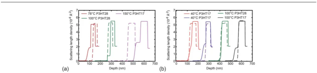
Having established the reproducibility of the brush layer, samples were annealed for different periods. In Fig. 2, we show volume fraction-depth proles for some samples at different temperatures and annealing times. It is clear that annealing has an important effect onlm morphology, although there is no clear effect of the molecular mass of the P3HT. The deformation of the interface was not observed on any of the as-cast samples, and is therefore a consequence of the annealing process. Changes in interfacial structure in these bilayers are due to either lateral roughness (for example, caused by capillary waves at a liquid–liquid interface), or interpenetration of at least one component into the other. We propose that interpenetration of the P3HT layer by the brush is most likely to be the cause of what is observed here; the P3HT cannot easily penetrate the dPMMA brush because the brush would have difficulty swelling to accommodate it. Capillary waves have a sinusoidal or near-sinusoidal interfacial prole, and so are not responsible for the structure observed here. Furthermore, the length scale of the interpenetration is too large for capillary waves (unless the sample dewetted), and in any case, the P3HT is expected to have large regions of crystallinity14,15which could not be treated
as a liquid surface, and thus exhibit such capillary waves. The step-like shape of the prole allows speculation that the dPMMA is penetrating grain boundaries and other defects in crystalline regions of the P3HT. Certainly, P3HT exhibits crys-talline behaviour at the annealing temperatures performed here, even down to 40C.16The exact molecular mechanisms of
Fig. 1 Reflectivity g per molta andfits for (unannealed) samples of (a) P3HT17 and (b) P3HT28 on dPMMA brushes of different thickness,t3. The data are plotted as Rk4(k) to allow a better assessment of the quality of thefits, and the data are staggered by factors of 10 for purposes of clarity.
Fig. 2 Scattering length density as a function of depth for P3HT on dPMMA brushes after annealing for (a) 5 min and (b) 24 h. Data are offset horizontally for clarity, and dashed lines are for the corresponding unannealed samples. The silicon substrate is to the right of each profile, and the P3HT layer on the left hand side. Two different samples are shown for P3HT17 annealed for 24 h at 40C. These allow for a test of reproducibility.
Open Access Article. Published on 10 September 2013. Downloaded on 24/06/2014 14:45:31.
This article is licensed under a
[image:4.595.54.553.427.532.2] [image:4.595.41.554.574.692.2]how such structural rearrangements can proceed is difficult to understand given that PMMA has a glass transition temperature in excess of 100C. It is known that thinlms of PMMA on gold exhibit depressed glass transition temperatures,17 but the
effects of the (molecular) mobility of amorphous polymers below the glass transition contains many open questions.
In Fig. 3 Scanning force microscopy (SFM) images (obtained in tapping mode using a MultiMode Digital Instruments atomic force microscope) of three samples are shown. An as-castlm on a silicon substrate (Fig. 3a) is notably rough, but the annealed lms are smoother. The large roughness seen in the as-cast surface in Fig. 3a is a (non-equilibrium) remnant of the spin-coating process. The amplitude of this roughness greatly reduces on annealing as seen in Fig. 3b and c. For these annealed samples (Fig. 3b and c), which have different P3HT
lms on the PMMA brushes, similar results are observed. Iso-lated defects are apparent in the annealed structures in Fig. 3b
and c, taking the form of depressions in the surface of the order of a few nanometres. The origin of these defects is not clear; their small size means that they may even be present in the unannealed samples. Because these defects have a depth that is much less than the typical brush thickness, they do allow some brush penetration, but this should not affect the integrity of the device. Aside from these defects, the surface is otherwise considerably smoother than the as-castlm. We do not have information on the (buried) P3HT interface with the polymer brush, but experimental studies of different P3HT interfaces have previously been reported and there can be more or less crystallinity at the buried interface compared to the free surface, depending on the surface in which the P3HT contacts.18
Regioregularity and molecular weight play key roles in the degree of crystallinity, and the orientation of crystalline lamellae in P3HT thinlms.19Previous work, in which P3HT is
spin-coated from a variety of solvents onto different substrates,
Fig. 3 Scanning force microscopy images of P3HT layers: (a) P3HT17 unannealed spin-coated onto a silicon substrate; (b) P3HT17 annealed at 100C for 24 h; and (c) P3HT28 annealed at 100C for 24 h. 5mm height scans are indicated for the region covered by the white line in each image.
Fig. 4 Output characteristics of P3HT22 (a–c) and P3HT42 (d–f) FETs with PMMA brushes on SiO2as gate insulators. (a) and (d) Reference samples, using a 700
nm-thick PMMAfilm spin-coated fromn-butyl acetate rather than a brush, and with no heat treatment before or after P3HT deposition (threshold voltage,VT¼ 5.6 and
13.3 V respectively); (b) and (e) samples annealed at 40C for 24 h (VT¼ 7.2 and14.6 V respectively); and (c) and (f) samples annealed at 100C for 5 min (VT¼
0.3 and9.8 V respectively). The gate voltages areVg¼0,20,40, and60 V and are indicated by red, blue, green, and black curves respectively. Threshold
voltages are obtained from theId1/2(Vg) transfer characteristics in the saturated regime (Vd¼ 60 V).
Paper Journal of Materials Chemistry C
Open Access Article. Published on 10 September 2013. Downloaded on 24/06/2014 14:45:31.
This article is licensed under a
Creative Commons Attribution 3.0 Unported Licence.
[image:5.595.68.530.269.426.2] [image:5.595.50.546.468.671.2]has shown (for the ranges of molecular weights and regior-egularity that we have used in the present study) that the P3HT (100) direction is usually normal to the substrate in blends, bilayers and pure P3HT layers.15,18–22Annealing does not affect
this crystal orientation with respect to the substrate, but has the effect of increasing the volume fraction of crystalline regions and the crystallite size and perfection.20In the present study we
do not know how the mixing at the interface affects the crys-talline structure, but previous studies have shown that mixing
within the amorphous P3HT fraction in a bilayer geometry, does not disrupt the organisation of the crystalline P3HT domains.22
3.2 Output characteristics
In order to determine whether the structural evolution of the interface upon annealing has any practical consequences for real devices, the output characteristics for devices fabricated with two different P3HT molecular weights are shown in Fig. 4. The thin dielectric allows these devices to operate at low volt-ages (less than 5 V). Transfer characteristics reveal threshold voltages,VT, that are typically between 0 and 10 V, and these are
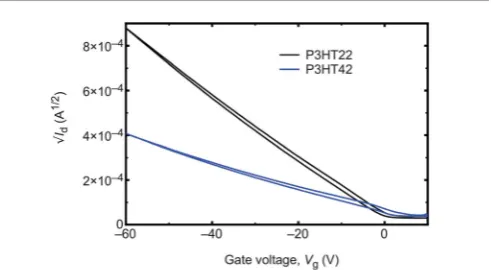
noted for some devices in the caption to Fig. 4. (All are included in the ESI.†) Example transfer characteristics are shown in Fig. 5. Generally, the devices using P3HT22 provide the smallest values ofVT. Furthermore, these devices also have signicantly
better output characteristics, suggesting that the effective capacitance of the brush layer is reduced due to traps in the P3HT42-based devices, possibly due to a less effective active layer. Certainly the quality of the P3HT lm is playing an important role in the device behaviour.
The C–V measurements (Fig. 6) indicate a low turn-on voltage. The sharp slope atVg¼0 indicates a low trap density.
The areal capacitance measured atVg¼ 35 V is normalized to
the calculated value of 9.20.2 nF cm2, which is for PMMA grown on silicon dioxide. The mobilities obtained from the transfer characteristics, for both long and short time annealing and for the two different molecular weights of P3HT tested, as well as reference unannealed devices are shown in Fig. 7. Values for carrier mobilities are found in the range of 3104to 2 103 V cm1 s1, with the annealing treatment affecting the P3HT42 samples more than the P3HT22 samples. In earlier studies using a silicon dioxide gate dielectric,23,24it was noted
that smaller mobilities are found for the lower molecular weight P3HT, in contrast to what we observe here. We do note, however, that the mobilities are of a similar order of magnitude to those in the earlier work, and also that the polymers in the earlier work were of lower molecular weights than those we have used here.23 More recent research has shown that P3HT
mobility in space-charge-limited current devices is greatest at a P3HT (number average) molecular weight of 12 kg mol1.25
The performance of the devices aer annealing at 40C is similar, indicating that the P3HT is of a similar quality. However, the mobility of the P3HT42 decreases with annealing
Fig. 5 Transfer characteristics for samples with P3HT brushes on SiO2as gate
insulators after annealing at 100C for 24 h (VT¼ 0.3 and 4.4 V for the P3HT22
and P3HT42 respectively). In these experiments,Vd¼ 60 V.
Fig. 6 Capacitance (C–V) results for a PMMA brush grown from a (300 nm) silicon dioxide layer. These data were obtained using P3HT42 as the semi-conductor layer.
Fig. 7 Saturated hole mobility data as a function of annealing temperature for 5 minutes annealing (a) and for 24 h annealing (b). The samples“annealed”at 22C are unannealed reference samples (a 700 nm spin coated PMMA layer rather than a brush); the temperature represents room temperature.
Open Access Article. Published on 10 September 2013. Downloaded on 24/06/2014 14:45:31.
This article is licensed under a
[image:6.595.47.293.167.302.2] [image:6.595.47.289.356.533.2] [image:6.595.42.555.587.702.2]whilst that of the P3HT22 sample is a little larger than the reference sample on the 700 nm PMMA lm, although no systematic temperature dependence can be stated. The likeli-hood here is that the shorter P3HT is better able to order due its larger (molecular) mobility during annealing.
It should not be concluded that a rough interface, or one with a complex structure, would result in a device of poor quality. Recent work has shown that non-uniform interfaces do not preclude good performance when P3HT is blended with an amorphous polymer.26Our system may well have an interfacial
structure not very different to the blend study, which indicates that the main requirement being that any crystalline regions of P3HT be connected to each other well enough through, for example, tie-lines or amorphous regions of P3HT.26
4
Conclusions
We have used neutron reectometry to demonstrate that a PMMA brush gate dielectric will penetrate the active P3HT layer aer annealing, even at temperatures as low as 40C. Device performance has been measured and output characteristics are not adversely affected by heat treatment. It is known that the addition of amorphous polymers into the active layers of organic FETs does not necessarily adversely affect device performance27and this is supported by the neutron data
illus-trating the penetration of the active layer by the gate. Saturated hole mobilities are, however, affected by heat treatment, with one sample exhibiting a small increase in mobility compared to the reference sample, and the other with a decrease in mobility on increased annealing.
Acknowledgements
We acknowledge the EPSRC for funding through GR/S96920/01. This project was supported by the European Commission under the 6th Framework Programme through the Key Action: Strengthening the European Research Area, Research Infra-structures (RII3-CT-2003-505925).
References
1 Z. Bao,Adv. Mater., 2000,12, 227–230.
2 H. Klauk,Chem. Soc. Rev., 2010,39, 2643–2666.
3 K.-J. Baeg, A. Facchetti and Y.-Y. Noh,J. Mater. Chem., 2012,
22, 21138–21143.
4 S. S. Chang, A. B. Rodr´ıguez, A. M. Higgins, C. Liu, M. Geoghegan, H. Sirringhaus, F. Cousin, R. M. Dalgliesh and Y. Deng,SoMatter, 2008,4, 2220–2224.
5 Y.-Y. Noh, N. Zhao, M. Caironi and H. Sirringhaus, Nat. Nanotechnol., 2007,2, 784–789.
6 J. Veres, S. Ogier and G. Lloyd,Chem. Mater., 2004,16, 4543– 4555.
7 J. C. Pinto, G. L. Whiting, S. Khodabakhsh, L. Torre, A. B. Rodr´ıguez, R. M. Dalgliesh, A. M. Higgins, J. W. Andreasen, M. M. Nielsen, M. Geoghegan,
W. T. S. Huck and H. Sirringhaus,Adv. Funct. Mater., 2008,
18, 36–43.
8 I. M. Rutenberg, O. A. Scherman, R. H. Grubbs, W. Jiang, E. Garfunkel and Z. Bao, J. Am. Chem. Soc., 2004, 126, 4062–4063.
9 L.-L. Chua, P. K. H. Ho, H. Sirringhaus and R. H. Friend,Adv. Mater., 2004,16, 1609–1615.
10 R. A. L. Jones, L. J. Norton, K. R. Shull, E. J. Kramer, G. P. Felcher, A. Karim and L. J. Fetters, Macromolecules, 1992,25, 2359–2368.
11 M. Sferrazza, C. Xiao, R. A. L. Jones, D. G. Bucknall, J. Webster and J. Penfold,Phys. Rev. Lett., 1997,78, 3693–3696.
12 S. Edmondson, V. L. Osborne and W. T. S. Huck,Chem. Soc. Rev., 2004,33, 14–22.
13 B. Zhao and W. J. Brittain,Prog. Polym. Sci., 2000,25, 677– 710.
14 M. Brinkmann,J. Polym. Sci., Part B: Polym. Phys., 2011,49, 1218–1233.
15 E. Verploegen, R. Mondal, C. J. Bettinger, S. Sok, M. F. Toney and Z. Bao,Adv. Funct. Mater., 2010,20, 3519–3529. 16 Y. Zhao, G. Yuan, P. Roche and M. Leclerc,Polymer, 1995,36,
2211–2214.
17 J. L. Keddie, R. A. L. Jones and R. A. Cory,Faraday Discuss., 1994,98, 219–230.
18 W. Porzio, C. Scavia, L. Barba, G. Arrighetti and S. Milita,Eur. Polym. J., 2011,47, 273–283.
19 H. Sirringhaus, P. J. Brown, R. H. Friend, M. M. Nielson, K. Bechgaard, B. M. W. Langeweld-Voss, A. J. H. Spiering, R. A. J. Janssen, E. W. Meijer, P. Herwig and D. M. de Leeuw,Nature, 1999,401, 685–688.
20 H. W. Ro, B. Akgun, B. T. O'Connor, M. Hammond, R. J. Kline, C. R. Snyder, S. K. Satija, A. L. Ayzner, M. F. Toney, C. L. Soles and D. M. DeLongchamp,
Macromolecules, 2012,45, 6587–6599.
21 S. T. Salammal, E. Mikayelyan, S. Grigorian, U. Pietsch, N. Koenen, U. Scherf, N. Kayunkid and M. Brinkmann,
Macromolecules, 2012,45, 5575–5585.
22 N. D. Treat, M. A. Brady, G. Smith, M. F. Toney, E. J. Kramer, C. J. Hawker and M. L. Chabinyc,Adv. Energy Mater., 2011,1, 82–89.
23 R. J. Kline, M. D. McGehee, E. N. Kadnikova, J. Liu and J. M. J. Fr´echet,Adv. Mater., 2003,15, 1519–1522.
24 A. Zen, J. Paum, S. Hirschmann, W. Zhuang, F. Jaiser, U. Asawapirom, J. P. Rabe, U. Scherf and D. Neher, Adv. Funct. Mater., 2004,14, 757–764.
25 C. R. Singh, G. Gupta, R. Lohwasser, S. Engmann, J. Balko, M. Thelakkat, T. Thurn-Albrecht and H. Hoppe, J. Polym. Sci., Part B: Polym. Phys., 2013,51, 943–951.
26 G. Lu, J. Blakesley, S. Himmelberger, P. Pingel, J. Frisch, I. Lieberwirth, I. Salzmann, M. Oehzelt, R. di Pietro, A. Salleo, N. Koch and D. Neher,Nat. Commun., 2013,4, 1588. 27 M.-B. Madec, D. Crouch, G. Rincon Llorente, T. J. Whittle, M. Geoghegan and S. G. Yeates,J. Mater. Chem., 2008,18, 3230–3236.
Paper Journal of Materials Chemistry C
Open Access Article. Published on 10 September 2013. Downloaded on 24/06/2014 14:45:31.
This article is licensed under a
Creative Commons Attribution 3.0 Unported Licence.