City, University of London Institutional Repository
Citation
:
Pornsuwancharoen, N., Youplao, P., Aziz, M. S., Ali, J., Amiri, S., Punthawanunt,
S., Yupapin, P. and Grattan, K. T. V. (2018). In-situ 3D Micro-sensor Model using Embedded
Plasmonic Island for Biosensors. Microsystem Technologies, doi:
10.1007/s00542-018-3798-1
This is the accepted version of the paper.
This version of the publication may differ from the final published
version.
Permanent repository link:
http://openaccess.city.ac.uk/19152/
Link to published version
:
http://dx.doi.org/10.1007/s00542-018-3798-1
Copyright and reuse:
City Research Online aims to make research
outputs of City, University of London available to a wider audience.
Copyright and Moral Rights remain with the author(s) and/or copyright
holders. URLs from City Research Online may be freely distributed and
linked to.
In-situ 3D Micro-sensor Model using Embedded Plasmonic
Island for Biosensors
N. Pornsuwancharoen
1, P. Youplao
1, M.S. Aziz
2, J. Ali
2, I.S. Amiri
3, S. Punthawanunt
4, P. Yupapin
5, 6*,
K.T.V. Grattan
71Department of Electronics Engineering, Faculty of Industry and Technology,
Rajamangala University of Technology Isan, Sakon Nakhon Campus, Sakon Nakhon, 47160, Thailand;
2Physics Department, Faculty of Science, Universiti Teknologi Malaysia, 81310 Johor Bahru, Malaysia; 3Division of Materials Science and Engineering, Boston University, Boston, MA, 02215, USA; 4Interdisciplinary Research Center, Faculty of Science and Technology, Kasem Bundit University,
Bangkok 10250, Thailand;
5Computational Optics Research Group, Advanced Institute of Materials Science, Ton Duc Thang University,
District 7, Ho Chi Minh City, Vietnam;
6Faculty of Electrical & Electronics Engineering, Ton Duc Thang University, District 7,
Ho Chi Minh City, Vietnam;
7Department of Electrical & Electronic Engineering, School of Mathematics, Computer Science & Engineering,
City,
University of London, Ec1V 0HB, United Kingdom;
*Corresponding author E-mail: [email protected]
Abstract:
The design of the microsensor system for biosensors using the plasmonic island is proposed. The sensor head is formed by the stacked layers of silicon-graphene-gold materials. The dual-mode operations of the sensor can be performed using the relationship of the changes between the electron mobility and optical phase, where the exciting environment can be light intensity(phase), electrical transient, heat, pressure, flavour and smoke, The change in light phase(intensity) in silicon and conductivity(mobility) in gold layers cause change in the output measurands. The design and simulation interpretation of the sensor is presented. The sensor manipulation using the MCM arrangement is simulated and interpreted for biosensor applications 3D imaging can also be applied to the MCM function, where the 3D in situ sensor function is possible. The sensor sensitivity of 2.0 x 10⁻²¹𝑐𝑐𝑐𝑐2𝑉𝑉−1𝑠𝑠−1 (𝑐𝑐𝑚𝑚)−1 via simulation is obtained.
Keywords: Microring sensors; Biosensors; Enviromental sensors; Plasmonic sensors; 3D sensors; Dual-mode sensors
1. Introduction
optical or electrical signals, while the medium of both applications is the light fields that can be coupled by either electrons or photons. In this article, we have designed a system that can be used to detect the change in the electrical or optical quantities, especially, intensity(or phase) of light or electrical mobility(of current) for the specific points . We are presenting a simulation based investigation, however, the used parameters are closed to the existing device fabrication technologies. By using the graphical method using Optiwave, followed by the mathematical simulation via Matlab program, the problem can be easily solved and the simulation results obtained. The sensor manipulation is demonstrated by changing the reflection coefficients of the microring conjugate mirror material, which is the TiO2 [Wang et al., 2003; Faruki et al., 2016]. The change in the relationship between the electron mobility and the input power due to the stimuli environment of the sensor system is the sensor sensitivity. The 3D image of the activity between the sensor and the stimuli is formed by the add port output, which is the FWM output of the MCM, in which the 3D image can be formed by the 3D imaging recovery system [Phattharacorn et al., 2016; Phathracorn et al., 2018; Chaiwong et al., 2017].
2. Background
We understand that mathematical complexity is not necessary to obtain simulation results. By using graphical approach, the required parameters can be acquired and used in the existing equations. Simple mathematical formulae can be used to obtain required results. In this work, the whispering gallery mode is the required of the system shown in Figure 1(a, b). The acquired parameters are then be used to perform the mathematical simulations. The optical field (E) propagates thorugh the microring system as shown in Figure 1(a) is given by equations (1)-(3) [Phattharacorn et al., 2016; Amiri et al., 2012].
𝑬𝑬𝒛𝒛= 𝑬𝑬𝒊𝒊𝟏𝟏= 𝑬𝑬𝟎𝟎𝒆𝒆−𝒊𝒊𝒌𝒌𝒛𝒛𝒕𝒕−𝝎𝝎𝒕𝒕 (1)
Where 𝐸𝐸0 is the electric field amplitude (real), 𝒌𝒌𝒛𝒛 is the wave number in the direction of propagation and 𝝎𝝎 is the angular frequency.
𝑬𝑬𝒕𝒕𝟏𝟏=𝑨𝑨𝑬𝑬𝒊𝒊𝟏𝟏-𝑩𝑩𝑬𝑬𝒊𝒊𝟐𝟐𝒆𝒆
−𝜶𝜶 𝟐𝟐𝑳𝑳𝟐𝟐−𝒋𝒋𝒌𝒌𝒏𝒏𝟐𝟐𝑳𝑳�
𝑪𝑪𝑬𝑬𝒊𝒊𝟏𝟏�𝒆𝒆 −𝜶𝜶
𝟐𝟐𝑳𝑳𝟐𝟐−𝒋𝒋𝒌𝒌𝒏𝒏𝑳𝑳𝟐𝟐�
𝟐𝟐
+𝑫𝑫𝑬𝑬ì𝟐𝟐�𝒆𝒆 −𝜶𝜶
𝟐𝟐𝑳𝑳𝟐𝟐−𝒋𝒋𝒌𝒌𝒏𝒏𝑳𝑳𝟐𝟐�
𝟑𝟑
𝟏𝟏−𝑭𝑭�𝒆𝒆−𝜶𝜶𝟐𝟐𝑳𝑳𝟐𝟐−𝒋𝒋𝒌𝒌𝒏𝒏𝑳𝑳𝟐𝟐�
𝟐𝟐 � (2)
𝑬𝑬𝒕𝒕𝟐𝟐 =𝒙𝒙𝟐𝟐𝒚𝒚𝟐𝟐𝑬𝑬𝒊𝒊𝟐𝟐 x
⎣ ⎢ ⎢ ⎢ ⎢
⎡𝒙𝒙𝟏𝟏𝒚𝒚𝟐𝟐�ĸ𝟏𝟏ĸ𝟐𝟐𝑬𝑬𝟎𝟎𝒓𝒓𝑬𝑬𝒊𝒊𝟏𝟏�𝒆𝒆 −𝜶𝜶
𝟐𝟐𝑳𝑳𝟐𝟐−𝒋𝒋𝒌𝒌𝒏𝒏𝑳𝑳𝟐𝟐�+𝒙𝒙𝟏𝟏𝒙𝒙𝟐𝟐𝟐𝟐𝒚𝒚𝟏𝟏𝒚𝒚𝟐𝟐�ĸ𝟐𝟐𝑬𝑬𝟎𝟎𝒓𝒓𝑬𝑬𝟎𝟎𝑳𝑳𝑬𝑬
𝒊𝒊𝟐𝟐�𝒆𝒆−𝜶𝜶𝟐𝟐𝑳𝑳𝟐𝟐−𝒋𝒋𝒌𝒌𝒏𝒏𝑳𝑳𝟐𝟐� 𝟐𝟐
𝟏𝟏−𝒙𝒙𝟏𝟏𝒙𝒙𝟐𝟐𝒚𝒚𝟏𝟏𝒚𝒚𝟐𝟐𝑬𝑬𝟎𝟎𝒓𝒓𝑬𝑬𝟎𝟎𝑳𝑳�𝒆𝒆 −𝜶𝜶
𝟐𝟐𝟐𝟐−𝒋𝒋𝒌𝒌𝒏𝒏𝑳𝑳 𝑳𝑳𝟐𝟐�
𝟐𝟐 ⎦ ⎥ ⎥ ⎥ ⎥ ⎤ (3)
Where 𝑥𝑥1=�1− 𝛾𝛾1, 𝑥𝑥2=�1− 𝛾𝛾2, 𝑦𝑦1=�1− ĸ1,𝑦𝑦2=�1− ĸ2, 𝐴𝐴= 𝑥𝑥1𝑥𝑥2, 𝐵𝐵= 𝑥𝑥1𝑥𝑥2𝑦𝑦2�𝑘𝑘1𝐸𝐸0𝐿𝐿, 𝐶𝐶=
𝑥𝑥12𝑥𝑥2ĸ1√ĸ2𝐸𝐸0𝑟𝑟𝐸𝐸0𝐿𝐿, 𝐷𝐷= (𝑥𝑥1𝑥𝑥2)2𝑦𝑦1𝑦𝑦2√ĸ1ĸ2𝐸𝐸0𝑟𝑟𝐸𝐸0𝐿𝐿2, F =𝑥𝑥1𝑥𝑥2𝑦𝑦1𝑦𝑦2𝐸𝐸0𝑟𝑟𝐸𝐸0𝐿𝐿. The other positions of the electrical field outputs
within the system can also be found, where the mathematical formulas are be found the give reference [Phatharacorn et al., 2018]. Under specific conditions, add port output can be observed due to reflection (feedback), where in this work the TiO2 lengths are used to obtain the required optical power reflection[Chaiwong et al. 2017; Phatharacorn et al., 2018]. However, the energy conservation of the system must be satisfied, hence, the normalized system is applied, where the normalized condition of the the input and output power for the remaining power. The remain output from the other ports are always found.
The 3D image construction, reconstruction and display is also presented in this work, which can be performed by using the same system which is considered as the microring conjugate mirror(MCM). Phatharacom et al. [Phatharacorn, et al., 2016], report that the MCM can be formed when the reflected power from the through and drop ports are suitably selected. The image construction can be seen at the WGM output, while the image reconstruction is obtained at the add port. In case of remote image transmission, the link of the fiber optic cable is required, from which the output of the add port is input into the input port and displayed at the WGM output, which produces naked-eye perception. The proposed sensor can be used as the dual-mode sensor, which means that the applied external source can have optical or electrical parameters. The two modes are the optical or electrical modes that can be selected by different output detection systems, which are obtained by the quantity in terms of the optical phase
term as 𝝋𝝋 = 𝟐𝟐𝝅𝝅∆𝒏𝒏𝒆𝒆𝒆𝒆𝒆𝒆
𝝀𝝀 L, where ∆𝒏𝒏𝒆𝒆𝒆𝒆𝒆𝒆 is the change in the effective refractive index, L is the optical path difference, and λ is the
input source wavelength. The relationship between the light intensity (I), group velocity and the electron mobility can be expressed as 𝑰𝑰=𝑬𝑬𝟐𝟐 = ( 𝑽𝑽𝒅𝒅
𝝁𝝁)𝟐𝟐, which is defined by Vd = µE. When an electric field E is applied to the grating sensor and an electric current
specific conductance or electrical conductivity of the conductor (gold is 1.6x10⁸ W-1m-1) [Gall, 2016; Baccarani and Ostoja, 1975].
[image:4.612.78.299.166.314.2]The advantage of the modified add-drop filter with two side rings is that the nonlinear effect can offer the shorter output pulse width and easier WGM resonant output control than the original system [Phatharacorn et al., 2017, Pornsuwancharoen et al., 2017]. The sensitivity of the system can be obtained by the relationship between the electron mobility output and the applied current (input power). Moreover, the use of the proposed sensor system may be possible for biosensors, specifically, using gold nanoparticles for the detection of viruses (cells) [He et al., 2011; Lee et al., 2015; Foreman et al., 2015; Sharma and Dominic, 2018; Anker et al., 2008].
Figure 1: Schematiic of a photonic island structure, where where 𝑬𝑬𝒊𝒊𝒏𝒏, 𝑬𝑬𝒕𝒕𝒕𝒕, 𝑬𝑬𝒅𝒅𝒓𝒓𝒅𝒅𝒅𝒅, 𝑬𝑬𝑨𝑨𝒅𝒅𝒅𝒅are the electrical fields of the input, through, drop and add ports, 𝑹𝑹𝒍𝒍, 𝑹𝑹𝒓𝒓, 𝑹𝑹𝒅𝒅 are the rinh radii of the left, right and center rings, respectively, κs : compling coefficients are 0.5. Si: Silicon, 𝑹𝑹𝒔𝒔𝒊𝒊: Silicon ring radius, 𝑹𝑹𝒈𝒈𝒓𝒓: Graphene rin radius, 𝑹𝑹𝑺𝑺𝑨𝑨𝑺𝑺: Gold ring radius, 𝒕𝒕𝑨𝑨𝑺𝑺:Gold rod height
Figure 2: The Optiwave results, where the parameters are
𝑹𝑹𝒍𝒍=𝑹𝑹𝒓𝒓=𝟏𝟏.𝟐𝟐𝝁𝝁𝝁𝝁, 𝑹𝑹𝒅𝒅=𝟐𝟐.𝟎𝟎𝝁𝝁𝝁𝝁, 𝑹𝑹𝑺𝑺𝒊𝒊=𝑹𝑹𝑮𝑮𝒓𝒓=𝟏𝟏.𝟎𝟎𝝁𝝁𝝁𝝁, 𝑹𝑹𝑨𝑨𝑺𝑺=𝟏𝟏𝟎𝟎𝒏𝒏𝝁𝝁, 𝒕𝒕𝑨𝑨𝑺𝑺=𝟐𝟐𝟎𝟎𝟎𝟎𝒏𝒏𝝁𝝁, the thickness of 𝑺𝑺𝒊𝒊 and 𝑮𝑮𝒓𝒓𝑮𝑮𝒅𝒅𝒕𝒕𝒆𝒆𝒏𝒏𝒆𝒆 is 1 𝝁𝝁𝝁𝝁 and 10 𝒏𝒏𝝁𝝁, respectively, the input light power is 200 mW. The refractive index of the silicon is 1.46. The linear and nonlinear refractive indices of the GaAsInP/P are 3.14 and 1.30x10⁻¹³ m2W-1, respectively. The attenuation
coefficient of the waveguide is 0.1 dB (mm)-1.
3. Manipulation and Results
In a simulation, the manipulation of the proposed plasmonic circuit for biosensor with the 3D image presentation has been configured by using the change in the MCM reflected power.The used parameters satisfiy the practical microring parameters and the waveguide supported Q-factor[Bogaerts et al., 2012] . The TiO2 coated lengths on the waveguide ends at the throughput and drop ports were varied, which is configured as the change in the sensing mechanism during the measurement. The in-situ 3D image of the sensing mechanism can be captured and the image displayed by the naked-eye 3D imaging recovery. The used parameters are provided with the given in the related figure captions and the following content. The plot of the add port mobility visibility output with the reflected end TiO2 lengths from 100-600 nm is shown in Figure 3. This is the MCM output is obtained from the sensor unit, which is the reflected information of the image construction at the sensor head, which is shown the relationship between the mobility visibility output and the different TiO2 lengths. It will be selected to perform the required sensor sensitivity. The electron mobility in a gold material is 42.6 cm2 V-1 s-1 [Gall, 2016; Baccarani and Ostoja, 1975], the electron mass is
9.10 × 10⁻³¹ kilograms, the electron charge is 1.60 × 10⁻¹⁹ coulombs.The refractive index of the silicon is 1.46. The
linear and nonlinear refractive indices of the GaAsInP/P are 3.14 and 1.30x10⁻¹³ m2W-1, respectively. The attenuation
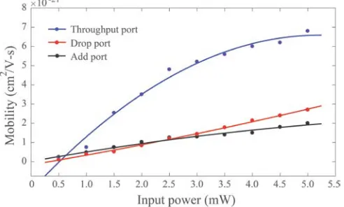
coefficient of the waveguide is 0.1 dB (mm)-1. The plot of relationship between the mobility output and input power
[image:4.612.316.540.167.302.2]integrated with the microscale device regime that can be used for cells or molecules sensors, while the live monitoring can be performed. In application, the MCM array can be integrated and the number of 3D pixels increased for large volume display.
Figure 3: The plot of the add port mobility visibility output with the reflected end TiO2 lengths, which was varied from 100-600 nm using the MATLAB program. The data points are the simulation result, where the solid line is the fitting curve.
Figure 4: The plot of the mobility output and input power of the through, drop and add ports at the source wavelenth of 1.55 µm, using the Equations (1)-(3) with the MATLAB program. The data points are the simulation results, where the solid lines are the fitting curves. The throughput and drop ports have shown the linear relationship, the sensor sesitivity 2.0 x 10⁻²¹𝑐𝑐𝑐𝑐2𝑉𝑉−1𝑠𝑠−1 (𝑐𝑐𝑚𝑚)−1 is obtained.
(a) (b) (c)
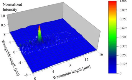
[image:5.612.185.431.307.455.2]Figure 5: Plots of the sensor activity manipulation by varying the TiO2 end lengths, using the Optiwave program. The add port outputs are plotted with the six TiO2 length and WGM power variations, where (a) 600 nm, (b) 500 nm, (c) 400 nm, (d) 300 nm, (e) 200 nm, (f) 100 nm. The 3D images of the six different measurement vales are plotted and seen, which is the manipulation of the sensing data.
4. Conclusion
We have proposed the use of the plasmonic island embedded within the MCM for the in situ 3D biosensors. The amount of change in cells quantities in response to the optical or electrical quantities tells about sensitivity of the sensor. We have manipulated the excited sensor environments by changing the MCM reflection coefficients to employ the sensor quantities. By the manipulating simulation, we have found that the change in the sensor head can be occured by the exciting environment related to the electron mobility or light incident energy. For an instant, the change in cells quantities related to the optical or electrical quantities can be formed the sensor sensitivity. We have manipulated the excited sensor environments by changing the MCM reflection coefficients to employ the sensor performance. The in-situ 3D image is also possible formed and presented by the output of the MCM, where the FWM signal outputs are input into the display system, the 3D image of the sensor is confirmed and displayed. The sensor sensitivity of 2.0 x 10⁻²¹𝑐𝑐𝑐𝑐2𝑉𝑉−1𝑠𝑠−1 (𝑐𝑐𝑚𝑚)−1 is obtained. Moreover, this system is not required the electronic 3D image reconstruction,
it is the naked-eye 3D display using the image recovery, which is the same as the initial input system.
Acknowledgment
:
M.S. Aziz would like to acknowledge the support and facilities through Flagship UTM Shine Project (03G82). P. Yupapin would like to acknowledge for the research facilities to Ton Duc Thang University, Vietnam.This isProf. Ali UTM Shine cost center number is Q.J130000.2426.03G82 (Flagship UTM Shine).
References
Aldawsari, S., Wei, L., Liu, W.K., 2015. Theoretical study of hybrid guided modes in a multilayer symmetrical planar plasmonic waveguide, J. Lightw. Technol., 33(15), 3198-3206.
Ali, J,., N. Pornsuwancharoen, Youplao, P., Aziz, M.S., Chiangga, S., Jaglan, J., Amiri, I.S., and P. Yupapin, 2018. A novel plasmonic interferometry and the potential applications, Results in Physics, 8, 438-411.
Amiri, I.S., Ali, J. and Yupapin, P.P., 2012. Enhancement of FSR and finesse using add/drop filter and panda ring resonator, J. Mod. Phys. B 26, 1250034.
Anker, J.N. , Hall, W.P., Lyandres, O., Shah, N.C., Zhao, J. and R.P. Van Duyne, R.P., 2008. Biosensing with plasmonic nanosensors, Nat Mat., 7(6), 422-453.
Baccarani, G. and Ostoja, P. 1975, Electron mobility empirically related to the phosphorus concentration in silicon, Solid State E lectron., 18(6), 579-580.
Bogaerts, W., Heyn, P.D., Vaerenbergh, T.V., Vos, K.D., Selvaraja, S.K., Claes, T., Dumon, P., Bienstman, P.,
Chaiwong, K. , Tamee, K., Punthawanunt, S. , Suhailin, F. H. , Aziz, M. S., Ali, J., Singh, G. and Yupapin, P., 2017. Naked-eye 3D imaging model using the embedded micro-conjugate mirrors within the medical micro-needle device. Microsystem Technologies 12(1), 1-5.
Hourhout, D.V. and Baets, R. 2012. Silicon micro-ring resonators, Laser Photon. Rev., 6910, 47-73.
Eurenius, L., Hagglund, C., Olsson, E., Kasemo, B. and Chakarov, D., 2008. Grating formation by metal-nanoparticle-mediated coupling of light into waveguided modes, Nature Photonics, 2, 360-364.
Faruki, M.J., Razak, M.Z.A., Azzuhri, S.R., Rahman, M.T., Soltanian, M.R.K., Rahman, B.M.A., Grattan, K.T.V., Rue, R.D.L. and Ahmad, H., 2016. Effect of titanium dioxide (TiO2) nanoparticle coating on the detection performance of microfiber knot resonator sensors for relative humidity measurement”, Material Express, 6, 501-508.
Felidj, N., Laurent, G., Aubard, J., Levi, G., Hohenau, F.A., Krenn, J.R. and Aussenegg, F.R., 2005. Grating-induced plasmon mode in gold nanoparticle, J Chem. Phys., 123(22), 221103.
Feng, J. V., Siu, S., Roelke, A., Mehta, V., Rhieu, S.Y., Tayhas, G., Palmore, R., Pacifici, D., 2011. Nanoscaleplasmonic interferometers for multispectral, high-throughput biochemical sensing, Nano Lett., 12(2), 602–609.
Foreman, M.R., Swaim, J.D. and Vollmer, F., 2015. Whispering gallery mode sensors, Adv. Opt. and Photon., 7, 168-240. Gall, D., 2016, Electron mean free path in elemental metals, J Appl. Phys., 119, 085101.
Hasan, Md. R., Akter, S., Rifat, A.A., Ahmed, K., Ahmed, R., Subbaraman, H., Abbott, D., 2018. Spiral photonics crystal fiber-based dual-polarized surface plasmon resonance biosensor, IEEE Sensors Journal, 18(1), 133-140.
He, L., Ozdemir, S.K., Zhu, J., Kim, W. and Yang, L., 2011. Detection single viruses and nanoparticles using whispering gallery microlasers, Nature Nanotechnology, 6, 428-432.
Lee, M.Y., Jackson, A.O. and Lee, L.K., 2015. Bioinspired optical antennas: gold plant viruses, Light; Science & Applications, 4, e267.
Li, D., Feng, J., Pacifici, D., 2016, Nanoscale optical interferometry with incoherent light, Scien. Rep., 2016, Article number 20836.
Morrill, D., Li, D. and Pacifici, D., 2010, Measuring subwavelength spatial coherence with plasmonic interferometry, Nature Photonics, 10, 661-687.
Phattharacorn, P., Chiangga, S., Ali, J. And Yupapin, P., 2018, Micro-optical probe model using integrated triple microring resonators for vertical depth identification, Microsystem and Technologies, Accepted.
Phatharacorn, P., Chiangga, S. and Yupapin, P., 2016. Analytical and simulation results of a triple micro whispering gallery mode probe system for a 3D blood flow rate sensor, Appl. Opt., 55(33), 009504.
Phatharaworamet, T., Teeka, C., Jomtarak, R., Mitatha, S. and Yupapin, P.P., 2010. Random binary code generation using dark-bright soliton conversion control within a Panda Ring resonator, J Lighwave Technol., 28(19), 2804-2809.
Pornsuwancharoen, N., Youplao, P., Amiri, I.S., and P. Yupapin, P., 2017(a). Electron driven mobility model by light on the stacked metal-dielectric-interfaces, Microw. & Opti. Techn. Lett., 59(7), 1704-1709.
Pornsuwancharoen, N., Amiri, I.S., Suhailin, F.H., Aziz, M.S., Ali, J., Singh, G. and Yupapin, P., 2017(b). Micro-current source generated by a WGM of light within a stacked silicon-graphene-Au waveguide, IEEE Photon. Technol. Lett., 29(21), 1768-1771.
Ren-Bing, T., Hua, Q., Xiao-Yu, Z., Wen, X., 2013, Electronics driven plasmon dispersion in AlGaN/GaN high electron mobility transistors, Chin. Phys. B, 22(11), 117306.
Sharma, A.K. and Dominic, A., 2018. Influence of chemical potential on graphene-based SPR sensor’s performance, IEEE Photonics Technology Letters, 30(1), 95-98.
Xiao, J.J., Yakubo, K. and Yu, K.W., 2006. Optical switching in graded plasmonic waveguides, Appl. Phys. Lett., 88, 241111.