University of Southampton Research Repository
ePrints Soton
Copyright © and Moral Rights for this thesis are retained by the author and/or other
copyright owners. A copy can be downloaded for personal non-commercial
research or study, without prior permission or charge. This thesis cannot be
reproduced or quoted extensively from without first obtaining permission in writing
from the copyright holder/s. The content must not be changed in any way or sold
commercially in any format or medium without the formal permission of the
copyright holders.
When referring to this work, full bibliographic details including the author, title,
awarding institution and date of the thesis must be given e.g.
UNIVERSITY OF SOUTHAMPTON
FACULTY OF SCIENCE, ENGINEERING & MATHEMATICS
Optoelectronics Research Centre
Direct UV-Written Waveguide Devices
by
Faisal Rafiq Mahamd Adikan
Thesis for the degree of Doctor of Philosophy
UNIVERSITY OF SOUTHAMPTON
ABSTRACT
Optoelectronics Research Centre
Doctor of Philosophy
Direct UV-Written Waveguide Devices
Faisal Rafiq Mahamd Adikan
This thesis describes a series of experimental studies concerning waveguide structures based on the direct UV and direct grating writing fabrication techniques. The latter approach allows simultaneous definition of waveguide structures and Bragg gratings.
The first result of this work describes the fabrication and characterisation of small angle X-couplers that exhibit low polarisation and wavelength dependence. Maximum and minimum coupling ratios of 95% (±0.8%) and 1.9% (±1%) respectively with typical excess loss of 1.0dB (±0.5dB) were recorded. Device modelling using Beam Propagation Method (BPM) and an analytical model showed good agreement with experimental results over a broad crossing angle and wavelength range.
By introducing refractive index asymmetry in 2° X-couplers, it was possible to tune the response to give a 50:50 coupling ratio. Multiple UV exposure experiments investigated the ‘proximity effect’ and provided further proof of the ability of UV writing to produce raised waist index X-couplers.
A first order Bragg grating electrically tunable via liquid crystal index modification with a maximum tunability of 141 GHz at 1562nm (TM polarised) and 114 GHZ at 1561.8nm (TE polarised) using electro-patterned ITO-coated glass electrodes is also presented. The 141GHz tuning range effectively covers up to five 25 GHz WDM channel spacing and was achieved with 170Vpp sinusoidal 1 kHz supply voltage. Hysteretic behaviour of the tuning curves was observed and is believed to be related to the dynamics of the disclination line formed along the waveguide axis with increase or decrease in supply voltage.
Contents
Abstract i
Fire Related Issues ii
Acknowledgments iii
1 Introduction 1
1.1 Thesis Structure ……… 3
References ……….. 6
2 Integrated Optics 7 2.1 Planar Waveguides: Device Functions & Applications ………... 10
2.1.1 Next Generation Technologies? ………... 12
2.2 S-bends, X-couplers & Bragg Gratings: Applications ………. 13
2.3 Summary ………... 16
References ……….. 18
3 Fabrication of Silica-Based Planar Waveguide Devices 21 3.1 Planar Deposition Techniques ………... 23
3.1.1 Thermal Oxidation ……… 24
3.1.2 Sol Gel ……….. 25
3.1.3 Plasma Enhanced Chemical Vapour Deposition (PECVD) ………. 26
3.1.4 Flame Hydrolysis Deposition (FHD) ………... 27
3.2 Waveguide Definition Techniques ………... 30
3.2.1 Photolithography & Etching ………... 30
3.2.2 Ion Exchange ………... 31
3.2.3 Femtosecond Direct Writing ………... 32
3.3 Direct UV Writing ……… 32
3.4 Summary ………... 35
References ……….. 36
4 Photosensitivity 39 4.1 Photosensitivity Mechanism ………. 40
4.2 Photosensitivity Dynamics ………... 43
4.3.1 Stability Issues ………. 45
4.4 Summary ………... 47
References ……….. 48
5 Waveguide, X-coupler & Bragg Grating Theory 50 5.1 The Slab Waveguide ………….……… 50
5.1.1 Marcatili Method ………. 57
5.1.2 Effective Index Method ………... 59
5.1.3 Beam Propagation Method ……….. 60
5.2 Analytical Model for Direct UV Written X-couplers ……….. 62
5.3 Bragg Grating Theory ………... 67
5.4 Summary ………... 70
References ……….. 71
6 Small Angle X-couplers 73 6.1 S-bends ………... 73
6.1.1 Experiment ……….. 78
6.1.2 Results & Discussion ……….. 79
6.2 Small Angle X-couplers ………... 82
6.2.1 Analytical & BPM Modelling ………. 84
6.2.2 Experiment ……….. 86
6.2.3 Results & Discussion ……….. 87
6.3 Tuning of Coupling Ratio via Asymmetry ………... 90
6.3.1 Experiment ………... 90
6.3.2 Results & Discussion ……….... 90
6.4 Summary ………... 92
References ……….. 93
7 Bragg Gratings as an Assessment Tool 95 7.1 Producing the Bragg Grating ……… 95
7.2 Experiment ……… 99
7.3 Results & Discussion ……… 100
7.4 Proximity Effect ………... 102
7.5 Summary ………... 105
8 Tunable Bragg Gratings via a Liquid Crystal Overlay 108
8.1 Liquid Crystals ………. 110
8.2 Device Assembly ……….. 112
8.3 Experiment ……… 114
8.4 Results & Discussion ……… 116
8.5 Anomalous Polarisation Behaviour ……….. 119
8.6 Effect of Supply Voltage Waveform ……… 122
8.7 Effect of Power Supply Frequency ………... 122
8.8 Electrode Offset ……….... 123
8.9 Thermal Effects ……….... 124
8.10 Applications ……… 126
8.11 Summary ………... 126
References ……….. 128
9 Flat Fibre Technology 130 9.1 MCVD Process ………... 131
9.2 Making the Flat Fibre ………. 132
9.3 Adding Waveguide Structures ……… 134
9.4 Propagation Loss Measurement – Experiment ………... 135
9.4.1 Results & Discussion ……….. 136
9.5 Substrate Analysis via Bragg Gratings ………... 138
9.6 Summary ………. 140
References ……….. 142
10 Conclusions & Future Work 143 10.1 Future Work ……… 144
References ……….. 148
Appendix A ORC FHD System Upgrade i
Appendix B FHD In Malaysia vi
List of Publications xi
Journal Papers
Flat Fibre Patent Application
Awards
Magazine Excerpts & Journal Appearance
i. Flat Fibre in Materials World ii. Flat Fibre in The Engineer
iii. Interview appearance in Nature Photonics
List of Tables
Chapter 2 Integrated Optics Page
2.1 Materials technology for integrated optical devices. 8
2.2 Typical optical or waveguide parameters of the various materials. 9
2.3 An example of the photonics value chain. 10
Chapter 3 Fabrication of Silica Based Planar Waveguide Devices
3.1 Summary of effect of dopants relative to pure silica. 29
3.2 DUW/DGW parameters and the corresponding device characteristics. 35
Chapter 6 Small Angle X-couplers
6.1 Comparison between various X-coupler experimental studies. 83
Chapter 7 Bragg Gratings as an Assessment Tool
7.1 FHD substrate specifications. 99
7.2 Absolute index increase for a given fluence level. 101
Chapter 8 Tunable Grating via Liquid Crystal Overlay
8.1 Nematic LC BDH 18523 specifications. 112
Constants
Symbol Name Value (unit)
µ0 Magnetic permeability of free space 4π x 10-7 (H/m)
ε0 Electric permittivity of free space 8.85 x 10⁻¹² (F/m)
h Planck’s constant 6.63 x 10⁻³⁴ (m2 kg/s)
eV Electron volt 1.60 x 10⁻¹⁹ (joules)
c Speed of light in vacuum 2.99 x 10⁸ (m/s)
Chemical Names
SiO2:Si silica-on-silicon
LiNbO3 lithium niobate
InGaAs indium gallium arsenide
InP indium phosphide
SiCl4 silicon tetrachloride
List of Figures
Chapter 2 Integrated Optics Page
2.1 Three types of planar waveguides: (a) rib, (b) ridge, and (c) buried. 10
2.2 (a) S-bend in a buried channel configuration, with the core layer sandwiched between two cladding layers; (b) Occurrence of transition and radiation (or bend) loss due to a curved waveguide.
13
2.3 (a) Schematic of X-coupler; (b) β is the crossing angle. 14
2.4 Schematic of three main functions of X-couplers: (a) power coupler; (b) 50% power splitter; (c) passive crossover.
14
2.5 Illustration of periodic refractive index perturbation in a channel waveguide, forming a grating structure.
15
2.6 Illustration of the operational properties of a reflection grating. 16
Chapter 3 Fabrication of Silica Based Planar Waveguide Devices
3.1 Schematic and photo of three layer silica-on-silicon sample. 23
3.2 Thin film deposition process steps. 23
3.3 Summary of sol gel processing. 25
3.4 PECVD deposition chamber and process schematic. 26
3.5 Schematic and photo of the deposition step of FHD. 28
3.6 The etching method process flow. 30
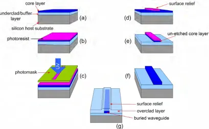
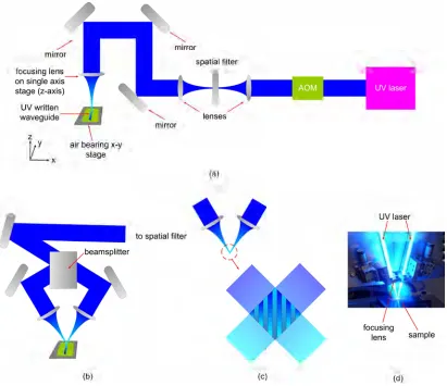
3.7 An illustration of (a) direct UV writing set up; (b) direct grating writing set up; (c) interference pattern generated by the crossed beam; (d) photo of direct grating writing.
33
Chapter 4 Photosensitivity
4.1 An illustration showing the tetrahedral structure of silica. 41
4.2 Colour centre model photosensitivity mechanism. 42
Chapter 5 Waveguide, X-coupler & Bragg Grating Theory
5.1 (a) Reflection and refraction at a plane interface, (b) light propagation in an index structure via total internal reflection (TIR) with evanescent field extending into the cladding layers.
51
5.2 Slab waveguide indicating a transverse field distribution Ey. z is direction of
propagation.
52
5.3 Graphical solutions to equations [5.29] and [5.30]. 56
5.4 Marcatili’s depiction of a channel waveguide index profile. 57
5.5 (a) Graphical solution of transcendental equation [5.37], (b) effect of asymmetry on the dispersion relationship for the fundamental TE mode.
60
5.6 Obtaining the effective index of the core by successively implementing the Effective Index method onto the various slab waveguides.
61
5.7 Schematic representation of the X-coupler and various supermodes. 63
5.8 Examples of calculated supermode field distribution. 66
5.9 (a) Output powers as a function of crossing angle; (b) output powers as a function of normalised profile height h (β = 1°).
67
5.10 Reflection spectra versus normalised wavelength (λ/λmax) for uniform gratings with various κL values.
70
Chapter 6 Small Angle X-couplers
6.1 A schematic showing various s-bend parameters. 74
6.2 (a) Cosine bend governed by f(x) = (D/2) (1-cos(πx/L)); (b) the continuously
varying curvature of the cosine bend.
77
6.3 Graphs showing modelled results of pure bend loss and transition losses using measured waveguide parameters.
77
measurements.
6.5 Optimised launch into channel waveguide with some scattered light in the slab waveguide as viewed by the IR camera situated along the output end of the sample.
79
6.6 Fibre-to-fibre loss with respect to s-bend curve radius. 80
6.7 X-coupler parameters. 82
6.8 Examples of BPM simulation of 1° crossing angle X-couplers with various waist index values.
85
6.9 Microscope and surface profiler images of a UV written X-coupler that has been etched to reveal the device structure.
86
6.10 Coupling ratio behaviour with respect to X-coupler crossing angle. 87
6.11 Wavelength dependencies of X-couplers for 3 different crossing angles. 88
6.12 Typical through and coupled power spectrum showing intensity dips at around 1370, 1480 and 1600nm.
89
6.13 Graph showing the coupling ratio against crossing angle using polarised input light, highlighting the low polarisation dependence of the structure.
89
6.14 A schematic representation of the fabricated UV written X-couplers with 2° crossing angle.
90
6.15 Coupling ratio and insertion loss of X-couplers with various second s-bend UV writing fluence values highlighting the effects of index asymmetry of the structure (solid and dotted lines: for indicative purpose only).
91
6.16 Wavelength dependencies of asymmetric X-couplers. 92
Chapter 7 Bragg Gratings as Assessment Tool
7.1 Schematic of the Direct Grating Writing technique. 96
7.2 Graph showing (a) reflection and (b) transmission spectra of a series of 1mm gratings direct UV-written with UV beam power of 50mW and 50% duty cycle.
98
7.3 Illustration of the experimental set up to assess planar Bragg grating reflection spectra.
99
7.4 Effective indexes versus UV writing fluence. Sample used: DN423/1. 100
7.5 Experimental layout of UV-written Bragg gratings and the previously defined channels for proximity effect characterisation (d: waveguide width).
103
7.6 Example of the gratings’ reflection spectra used for the proximity effect experiment.
103
7.7 Effective indexes at various spacing and fluence values. 104
7.8 Normalised profile height, h versus UV writing fluence. 105
Chapter 8 Tunable Grating via Liquid Crystal Overlay
8.1 Illustration of the molecular order in a nematic liquid crystal. 110
8.2 Illustration of (a) homeotropic and (b) homogeneous alignment. 111
8.3 Refractive index of the LC18523 with temperature at λ=1550nm (taken from [20]). 112 8.4 A schematic representation of the assembled device showing the liquid crystal
overlay in between the electro-patterned ITO electrodes and the waveguide containing Bragg gratings.
114
8.5 Photographs showing the HeNe scattering footprint of an etched segment of the sample containing planar Bragg gratings viewed from the top of the sample.
115
8.6 Device tuning curves for both TM and TE polarised light showing hysteresis between points A and B.
116
8.7 Grating reflection spectra at the two threshold points for increasing voltage values. 117 8.8 Grating spectrum observed in reflection with the fitted Lev-Mar curves shown. 118 8.9 Disclination line dynamics with applied voltage seen via 90° cross polarisers (data
was taken from experiments by Benjamin Snow).
119
8.10 Schematic depiction of expected LC alignment at initial and final voltage states, showing the anticipated refractive index ‘seen’ by TM and TE polarised light.
120
8.11 Transmission images from the output facet of the LC device at different instances during the increasing voltage sequence with TE polarised input light.
121
8.12 λB shift for TE polarised input at low voltages. 121
8.13 TE tuning curve with various supply voltage waveform. 122
(offset).
8.16 Graph showing the effect of electrode position with respect to waveguide on the tunability of the device.
124
8.17 Graphs showing λB as a function of temperature for: (a) experimental set up under room temperature conditions, (b) thermal behaviour of the assembly.
125
8.18 Effect of applying voltage across ITO electrodes at random points and duration along the experimental run, indicating that very little thermal effect is taking place.
126
Chapter 9 Flat Fibre Technology
9.1 Schematic representation of the preform fabrication stage of MCVD. 131
9.2 Schematic representation of the fibre drawing stage of MCVD. 132
9.3 (a) Cross section; and (b) perspective views of the novel flat fibre sample. 133
9.4 Extended lengths of the flexible glass planar substrate. 134
9.5 Image captures of (a) straight channel waveguide and (b) the two output arms of 100µm y-splitters, both illuminated at λ = 633nm.
134
9.6 Photographs of the pigtailed assembly for propagation loss measurements. 136 9.7 Schematic diagram of the optical set up for free space and fibre coupled
propagation loss measurement.
136
9.8 Cutback loss measurement results relating detected transmitted light to flat fibre length (curves with broken lines represent the linear fit).
137
9.9 SEM image of the core of the flat fibre with the arrow pointing to the boundary where the layers meet.
137
9.10 First demonstration of Bragg reflection in a flat fibre sample. The inset shows the ASE spectra of the input light and the Bragg gratings reflection.
138
9.11 Mean effective refractive index variation across the cross section of the sample core layer.
139
9.12 Birefringence of the flat fibre core layer with mean birefringence of ~3.3x10⁻⁴. 140
Chapter 10 Conclusions & Future Work
10.1 (a) Waveguide dimensions generated from red luminescence study, (b) detection of green and red luminescence that complement each other along the UV beam path.
145
10.2 (a) Bubble switch architecture employing X-coupler and groove geometry. (b) A distributed stress/strain sensor where the peak Bragg wavelength (and possibly the reflection amplitude) of the gratings is modified by applying force onto the waist region of the X-coupler.
146
10.3 Conceptual depiction of a fully flexible flat fibre distributed sensor. 147
Appendix A ORC FHD System Upgrade
A.1 Schematic representation of the FHD system. ii
A.2 Corrosion in the FHD chamber. iii
A.3 Top view of gas piping and electrical connections of the new FHD chamber control box.
iv, v
Appendix B FHD In Malaysia
B.1 Various defects/pores found on the fabricated 3-layer samples. vii
B.2 (a) HeNe set up for NA measurements and mode profiling, and (b) shows a typical mode profile of a waveguide with the data generated by the HeNe curve fitting program.
viii, ix
B.3 Numerical aperture of UV written channels with increasing UV writing fluence levels.
Abbreviations
AOM Acousto-optic Modulator
ASE Amplified Spontaneous Emission BPM Beam Propagation Method CTE Coefficient of Thermal Expansion CVD Chemical Vapour Deposition DBR Distributed Bragg Reflector DFB Distributed Feedback DGW Direct Grating Writing
DTI Department of Trade & Industry DUW Direct UV Writing
DWDM Dense Wavelength Division Multiplexing EDFA Erbium Doped Fibre Amplifier
EDWA Erbium Doped Waveguide Amplifier FBG Fibre Bragg Grating
FHD Flame Hydrolysis Deposition
GODC Germanium Oxygen Deficient Centre IP Internet Protocol
IR Infrared
ISP Internet Service Provider LC Liquid Crystal
LED Light Emitting Diode LEV-MAR Levenberg-Marquardt
MCVD Modified Chemical Vapour Deposition MFC Mass Flow Controller
MMI Multimode Interference
MOST Media Oriented Systems Transport MUX Multiplexer
NOV Neutral Oxygen Vacancy OADM Optical Add Drop Multiplexer OSA Optical Spectrum Analyser OVD Outside Vapour Deposition
PECVD Plasma Enhanced Chemical Vapour Deposition PL Photoluminescence
ROADM Reconfigurable Optical Add Drop Multiplexer SEM Scanning Electron Microscopy
UV Ultraviolet VoIP Voice Over IP
Acknowledgments
I am honoured to be part of this institution. Working at the Optoelectronics Research Centre has been tremendous and I have greatly enjoyed my stay here. My deepest gratitude goes to my supervisors – Prof. Peter Smith and Dr. Corin Gawith – for their support, advice, understanding, and more importantly, for making the decision to take me on board in the first place.
I am extremely grateful to Dr. James Gates for his part in the later stages of my research. Also, to other members of the group – past and present – Dr. Ian Sparrow, Dr. Gregory Emmerson, Dr. Denis Guilhot, Huw Major, Christopher Holmes, Benjamin Snow, Mario Ramirez, Dr. Samuel Watts, Dr. Lu Ming, and Dr. Dmytro Kundys.
Special thanks to Eve Smith and Dr. Eleanor Tarbox for their part in ensuring that I got everything done on time and efficiently.
I would also like to thank my colleagues at the ORC who have taught me so much, and for their assistance: Dr. Francesco Poletti, Rodrigo Amezcua, Andrew Webb, Dr. Jayanta Sahu, Dr. Neil Broderick, Ed Weatherby, Mark Lessey, Niel Fagan, Simon Butler, Dr. Peter Lanchester, Trevor Austin, Timothy McIntyre, Chris Nash, Kevin Sumner, Prof. David Payne, Neil Sessions, Mukhzeer Shahimin, Robert Simpson, Prof. Rob Eason, Tleyane Sono, and Robert Standish. Also, thank you to Rachel Abbott for her part in promoting the flat fibre.
I am also grateful to Prof. Harith Ahmad, Dr. Christos Riziotis, Dr. Malgosia Kaczmarek, Dr. Andriy Dyadyusha, Dr. Daniel Jaque and Dr. Mohd. Adzir Mahdi.
To my friends in the ORC, the Southampton Malaysian community, my colleagues in the University of Malaya, my wife Mazarisusanty Ibrahim and our two kids, Muaz Rafiq and Maisarah Rafiq, and to my family back home, I thank you. Big thanks to my parents, Mahamd Adikan Hasan and Patimah Ahmed, for their part in shaping me to be the person I am today.
Chapter 1
Introduction
The increasingly important role played by optical based technologies in general, and integrated optics in particular, is reflected in recent announcements of governmental backing, and market projections. For example, in 2005, the UK Science and Innovation Minister, Lord Sainsbury, announced a £100 million funding initiative under the Department of Trade and Industry (DTI) Technology Programme. Among the specific areas covered were a number of optical technologies such as next generation lasers, highlighting the field’s importance. This recognition of optics was followed by a recent report published by the DTI, aptly titled ‘Photonics: A UK strategy for success’, in which several strategic recommendations were underlined to advance the industry further, in order to strengthen the UK’s position in this important part of the world economy [1]. According to the US-based Optoelectronics Industry Development Association (OIDA), the overall global market growth of optoelectronics components and enabled products grew by the impressive figure of 39% in 2004, spurring heightened research interests [2].
event, although unfortunate, also fuelled a number of ventures into new markets for optical based technologies including optical sensors.
The concept of integrated optics was first introduced by S.E. Miller in 1969 [4]. It is not difficult to see why the idea was quick to find acceptance, particularly when it has the potential to be analogous to the far-reaching effects microelectronics had on the global market and technological developments. Integrated optics still has a long way to go to achieving this impact, not least in terms of the variety of material systems utilised to achieve a particular functionality. Among the many platforms, the most dominant material for optically passive functionalities that include basic signal routing, power splitting, and wavelength filtering, is silica, which is the same base material that is used for optical fibres.
Silica-based planar devices can be fabricated via numerous techniques (as described in Chapter 3 of this thesis). One of these is direct UV writing, which was demonstrated as early as 1974 [5], but only later found application in the silica platform in the early 90’s [6]. From then onwards, research based on the technique saw a marked increase, with the annual rate of journal publications rising from one in 1993 to sixteen in 2002 [7]. Direct UV writing is analogous to the computer numerical control (CNC) milling machining of metal parts. It involves defining waveguide structures by exposing a photosensitive silica sample to UV light. By translating the sample underneath the focussed UV beam, waveguide structures such as straight channels and y-splitters can be formed. The versatility of the technique was further enhanced by the introduction of the direct grating writing approach, which was developed here in the Optoelectronics Research Centre (ORC) [8]. This latest capability meant that waveguide structures and Bragg gratings could be defined simultaneously, allowing rapid prototyping of novel devices.
Following on from this unfortunate event, a number of alternative research avenues were sought, and subsequently achieved, mainly by collaborating with research groups within the ORC, and external institutions. The novel flat fibre substrate (Chapter 9) resulted from one such collaboration.
1.1
Thesis Structure
I have structured the thesis as follows.
In Chapter 2 an overview of integrated optics is presented, highlighting the motivation behind the mercurial development of the field as well as the challenges that need to be addressed in order to emulate the successes of electronics. There is a wide array of material system and design approaches that address specific needs such as light generation, passive components and detection. I have provided a brief comparison between these material systems in terms of their fabrication techniques, level of refractive index contrast achievable, and also the specific advantageous attributes displayed by each of them. A number of market reports and projections were also quoted, stressing the ubiquity of the technologies. Following from these, a closer look at practical implementation of the silica-based structures that were investigated in this research was presented. These structures are s-bends, X-couplers, and Bragg gratings. Further elaborations in terms of modelling and experimental work are presented in later chapters (see below).
Chapter 3 provides a review covering substrate fabrication methods and channel
definition techniques. The topic covers fabrication methods such as flame hydrolysis deposition, plasma enhanced chemical vapour deposition, and sol-gel. This is followed by a review of channel definition techniques including ion exchange, photolithography and etching, and direct UV writing. Direct UV writing is chosen as our channel definition technique and is exceptionally valuable in device prototyping as the technique requires no masks, does not involve a multi-stage process such as the one via photolithography and etching, and does not need clean room facilities. It does however require the samples to be photosensitive.
devices. One critical stage that we employ in processing our samples prior to UV writing is hydrogen loading, a low temperature high pressure technique that diffuses hydroxyl species into the glass matrix, allowing an increase in photosensitivity.
Chapter 5 presents theoretical treatment of slab and channel waveguides. Electrical
and magnetic field distribution as well as parameters governing single mode operation are obtained via solutions to Maxwell’s equations. This is followed by modelling of waveguide bends, relating bend radius to pure bend loss as well as the calculation of transition losses due to modal mismatches. A brief description of an analytical model of X-couplers, developed by Durr and Renner [10], is also covered in this chapter, where the empirical formula provided in their work was used to compare simulated and measured coupling behaviour of fabricated small angle X-couplers. I have also employed a commercially available beam propagation method simulation suite for the X-coupler work presented in
Chapter 6. For completeness, a brief description of this technique is provided. Chapter 5
concludes with a theoretical treatment of Bragg gratings, which were employed in work presented in Chapters 7, 8 and 9.
As mentioned above, Chapter 6 describes experimental work and analysis of UV-written s-bends and X-couplers. A comparative study on s-bends formed by joining two partial circles (circular s-bends) and cosine bends concludes that the cosine bends systematically display ~0.3dB lower fibre-to-fibre loss to that of the circular bends. This is attributed to transition losses of the circular bends. Following from this result, subsequent experiments involving the s-bend structure, including X-couplers and y-splitters, all utilise the cosine bend.
The fabrication and characterisation of small angle X-couplers is also presented in
Chapter 6. It is found that direct UV writing is ideal in producing a raised waist index
profile, an attribute which is important in ensuring good device performance. Good agreement between modelled and measured data was also obtained, with the X-couplers showing very low polarisation and wavelength sensitivity.
Up to this point, all the UV writing experiments described made use of the single-beam set up, and therefore the devices/structures fabricated do not contain Bragg gratings. In the remainder of this thesis, measurements and devices involving the gratings are described.
Chapter 7 elaborates the use of Bragg gratings as assessment tools. By interrogating
An electrically tunable planar Bragg grating using a liquid crystal overlay is described in Chapter 8. A tuning range encompassing at least five 25GHz spaced wavelength division multiplexed channels was achieved by applying 170Vpp across indium tin oxide electrodes. The use of an anisotropic nematic liquid crystal allows the modification of the overall structure’s effective index, which in turn is reflected in the peak Bragg wavelength shift. Such a device could be implemented in reconfigurable switching architectures.
I have described our patent-applied-for flat fibre technology in Chapter 9. The flat fibre substrate combines the inherent advantages of both standard optical fibres and planar silica-on-silicon. Functional structures including straight channels, y-splitters and Bragg gratings were successfully UV-written through ∼ 350µm thick cladding layer. Assessment of the core layer uniformity and the waveguide birefringence were also made.
Chapter 10 concludes this thesis. On-going research based on the devices presented
here is also described, along with some suggestions for future work.
References:
[1] DTI document entitled: "Photonics: A UK strategy for success," 2006. This document can be obtained from:
http://www.dti.gov.uk/sectors/electronicsit/ukphotonicsstrategy/page30715.html [2] O. I. D. A. (OIDA), "Opto Market Performs Well in 2004," in OIDA News, vol. 14,
2005, p. 1.
This document can be obtained from:
http://www.oida.org/pdfs/oidanews/oidanews0905.pdf
[3] V. Thomson, "Seeing the light – Optoelectronics market focus," in CHIP, 2002. [4] D. Marcuse, Integrated Optics, IEEE Press, New York, 1972.
[5] E. A. Chandross, C. A. Pryde, W. J. Tomlinson, and H. P. Weber, "Photolocking-A new technique for fabricating optical waveguide circuits," Applied Physics Letters, vol. 24, pp. 72-74, 1974.
[6] M. Svalgaard, C. V. Poulsen, A. Bjarklev, and O. Poulsen, "Direct UV writing of buried singlemode channel waveguides in Ge-doped silica films," Electronics
Letters, vol. 30, pp. 1401-1403, 1994.
[7] M. Svalgaard, "Direct UV-written integrated optical components," Optical Fiber
Communication Conference (OFC) 23-27 Feb. 2004, Los Angeles, CA, USA, paper FK2.
[8] G. D. Emmerson, S. P. Watts, C. B. E. Gawith, V. Albanis, M. Ibsen, R. B. Williams, and P. G. R. Smith, "Fabrication of directly UV-written channel waveguides with simultaneously defined integral Bragg gratings," Electronics
Letters, vol. 38, pp. 1531-1532, 2002.
[9] D. A. Guilhot, G. D. Emmerson, C. B. E. Gawith, S. P. Watts, D. P. Shepherd, R. B. Williams, and P. G. R. Smith, "Single-mode direct-ultraviolet-written channel waveguide laser in neodymium-doped silica on silicon," Optics Letters, vol. 29, pp. 947-949, 2004.
[10] F. Durr and H. Renner, "Analytical design of X-couplers," Journal of Lightwave
Chapter 2
Integrated Optics
It can be argued that integrated optics could be as revolutionary to classical optics as microelectronics is to electrical engineering. To date, the technological advancement of the field has resulted in the miniaturisation of traditional bulk optics and the introduction of multi-functional modules. From a historical perspective, the concept of integrated optics was first coined by S.E. Miller in 1969 who foresaw that technologically, integrated optical devices offer long term stability, increased immunity to thermal and environmental influences, and eliminate the alignment issues inherent in bulk or fibre based optics. So significant were the ideas that within three years, the IEEE1 published a reprint book on integrated optics containing principal ideas and contributions within the field from leading research workers, including Miller. In the book, he remarked that the growing interest in optical integration ran strong and that involvement in the field is ‘fruitful professionally and profitable economically’ [1]. The argument is that integration is the key towards transforming optics, just as integrated circuits on silicon transformed electronics, thus leading to a larger acceptance of the technology.
Another important motivation fuelling this technological progression lies in the inherent challenges faced in designing electronic circuits that can operate efficiently in the high frequency range offered by optical technologies (in the Tb/s regions). This stems from the frequency dependent attenuation level of metallic conductors that make up the interconnections within these electronic circuits.
It can also be argued that the economic attractiveness of integrated optics lies in the possibility of fully automated mass production. Low cost fabrication methods derived from the well established micro-electronics industry also played a role in expanding the field further. Having said that, there are challenges associated with the technology that offset these advantages such as the complexity of fibre-pigtailing the finished products, which tend to be labour intensive. Increasing the manufacturing yield or throughput of batch
manufactured integrated optical devices is also an issue where current typical yields of current devices tend to be in the region of 50-60% [2].
One of the biggest hurdles to overcome if integrated optics is to emulate the electronics success story is in combining the various material systems currently being used onto a single platform (what is termed as monolithic integration). This stems from the predominantly material specific device functions of optical components such as InGaAs2 for detectors, LiNbO3
3
for modulators, SiO2:Si 4
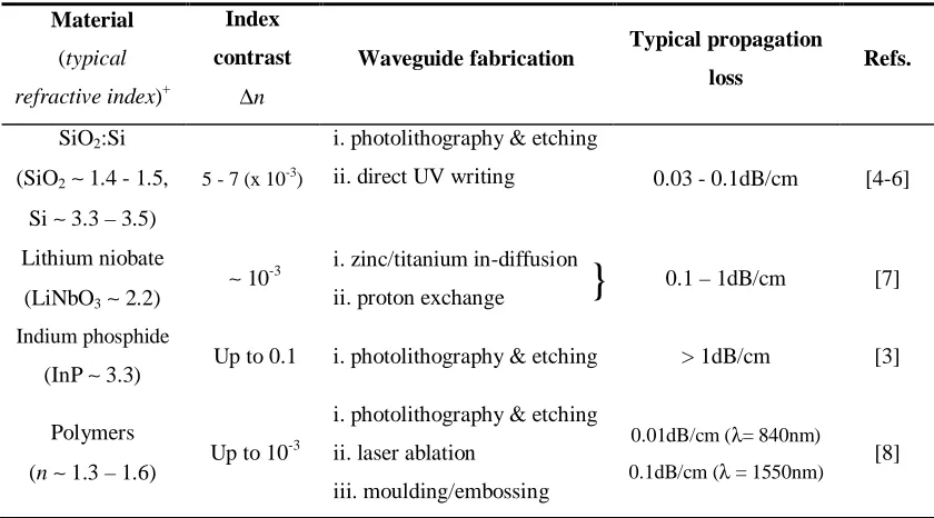
[image:21.595.108.531.322.566.2]for passive devices and interconnects. One expert suggested that the current state of integration in optics is similar to that of electronics in the 1970s [2]. Table 2.1, derived from reference [3], elucidates the above remarks, and Table 2.2 describes the typical optical characteristics of the various materials.
Table 2.1 Materials technology for integrated optical devices [taken from [3]].
Material Properties Fabrication Advantages Application
SiO2:Si
Cheap and versatile fabrication Thermal oxidation, CVD, or FHD Versatile, builds from the Microelectronic technology Passive devices (couplers, MUX), sensors, filters Lithium niobate Electro-optic, acousto-optic, non-linear, birefringent Metallic diffusion, proton exchange
Active control of
light, anisotropic
Switches,
modulators
III-V compounds
(InP, GaAs) Electro-optic Epitaxial growth
High level of
integration Detectors
Polymers Electro-optic,
thermo-optic Spin, dip coating
Wide range of
physical
properties
Sensors
CVD: chemical vapour deposition; FHD: flame hydrolysis deposition; MUX: multiplexer; InP:
indium-phosphide.
In this chapter, a review of the applications of these integrated devices is presented, with the aim of highlighting the breadth and importance of the technology. The emphasis will be, but not exclusively on, those devices that are based on the silica-on-silicon
2
InGaAs: indium gallium arsenide.
3
LiNbO3: lithium niobate. 4
}
[image:22.595.107.527.182.415.2]platform. This is the substrate used throughout this work. Needless to say, there are a wide range of components and devices that fall under the term integrated optics, and a similarly wide range of fields in which they are used.
Table 2.2 Typical optical or waveguide parameters of the various materials.
Material
(typical
refractive index)+
Index contrast
∆n
Waveguide fabrication Typical propagation
loss Refs.
SiO2:Si
(SiO2∼ 1.4 - 1.5,
Si ∼ 3.3 – 3.5)
5 - 7 (x 10-3)
i. photolithography & etching
ii. direct UV writing 0.03 - 0.1dB/cm [4-6]
Lithium niobate
(LiNbO3∼ 2.2)
∼ 10-3 i. zinc/titanium in-diffusion
ii. proton exchange 0.1 – 1dB/cm [7]
Indium phosphide
(InP ∼ 3.3) Up to 0.1 i. photolithography & etching > 1dB/cm [3]
Polymers
(n ∼ 1.3 – 1.6) Up to 10
-3
i. photolithography & etching
ii. laser ablation
iii. moulding/embossing
0.01dB/cm (λ= 840nm)
0.1dB/cm (λ = 1550nm) [8]
+
Typical refractive index values are usually quoted for λ = 633nm.
Table 2.3 An example of the photonics value chain [taken from [9]].
Materials & Process Equipment
Components Modules Service
Providers
Content &
Applications
Enabled
Products End User
Silica/Silicon GaAs InP Polymer Lasers Fibres Filters Detectors Mux/Demux LCDs Telecoms LEDs Solar cell Imaging Telecoms Energy Medical Telecoms Surveillance Sensing Entertainment Computers Phones Cameras Lighting Displays Business Consumer Government Military Medical
LCD: liquid crystal display; LED: light emitting diode; ISP: internet service provider; VoIP: voice
over internet protocol.
2.1
Planar Waveguides: Device Functions & Applications
There are three main types of waveguides named after their basic structural properties namely rib, ridge, and buried waveguides as illustrated in Fig. 2.1. The physics that dictates light guidance within these waveguides will be further discussed in Chapter 5. But for now it is sufficient to state that the waveguides fulfil the requirements needed to confine and guide light with sufficiently low losses. Most importantly, they have a core refractive index that is higher than the surrounding material (cladding). We use the buried waveguide type throughout this work (Fig. 2.1(c)).
Figure 2.1 Three types of planar waveguides: (a) rib, (b) ridge, and (c) buried.
• Interconnects: as the name suggests, these serve to optically connect two points/elements on an optical chip. If there is an offset needed between the two i.e. the two elements are not aligned to each other, then s-bends would be utilised (please refer to Section 2.2). In our case, we refer to these interconnects as channel waveguides.
• Power splitters: these usually split power from a single channel waveguide between two output ones. The simplest form of these elements is commonly referred to as y-splitters (or y-branch) due to their distinct y shape. An extension of this element would have more than two output branches and as such, the term 1xN splitter was adopted for generality where N is the number of output branches. Other similar elements that perform the same task are directional couplers, X-couplers (please refer to Section 2.2), and multimode interference (MMI) couplers.
• Filters/Reflectors: perform the task of reflecting light into a channel waveguide. If the band pass of such a reflector is of a particular wavelength, then this could also be viewed as performing the role of a filter. The simplest implementation of this is by using a mirror. However, a more attractive and widely used technique is by using a grating, which is inherently a wavelength selective element (please refer to Section 2.2).
A more exhaustive list of these basic functions can be found in reference [3].
gain equalisation filters [18] and waveguide mode lockers [19, 20]. This said, monolithic integration of all the required optically passive and active devices remains a challenge due to the various material-based functionalities, as mentioned earlier.
The telecommunications industry is not the only area where ubiquitous application of integrated optical devices takes place, and this was highlighted in Table 2.3. For example, solutions based on integrated optics such as lab-on-chip and micro-fluidics are now gaining an increasing foothold on the biosensor market, which is forecast to swell to £5.7 billion in 2007, with an annual growth rate of around 10 per cent [21]. In the increasingly important field of defence and homeland security, integrated optical sensors perform the role of detecting chemical and bio-hazardous substances such as anthrax. One of the biggest markets yet is in the consumer electronics and entertainment sector. Light emitting diode lighting, data storage technologies such as DVDs and Blu-ray are a few examples of the technologies found within this sector.
2.1.1
Next Generation Technologies?
Given the myriad developmental activities in the field, this progressive trend is expected to continue well into the next decade. There are a number of recent developments that are making waves within the research community in particular, including:
• Silicon optics: The potential for monolithic integration with microelectronics provides the main thrust in work in this field. Interest in the field grew tremendously following the demonstration of a silicon laser in late 2004 by Bahram Jalali of the University of California [22]. However, optical pumping is still a limitation and efforts in combining electrically pumped laser sources onto a silicon waveguide configuration are under way, including the recent demonstration by Fang et al [23].
• Surface plasmons: As a phenomenon, surface plasmons, which denotes electromagnetic surface waves that have their intensity maximum in the surface and exponentially decaying fields perpendicular to it, were first reported as early as 1957 [24]. Research on the field re-emerged with the advent of fabrication methods and the recent increasingly important role played by sensors, which is where the technology is likely to find wide deployment.
Theoretical treatment and experimental results on these devices are presented in Chapters 5 and 6 respectively.
2.2
S-bends, X-couplers & Bragg gratings: Applications
These simple but important optically passive waveguide structures are incorporated into optical modules to improve performance and in many cases, perform key tasks. S-bends are utilised as spatial mode filters [17] and spot-size converters [25, 26]. In semiconductor lasers, s-bends are used to increase the threshold for the first order mode, preventing multi-mode operation. Swint et al [17] measured an increase of 5-10% in threshold power to that of the conventional straight waveguide by using a cosine s-bend. Spatial mode filters in general exploit the fact that higher order modes have a larger fraction of their mode field propagating outside the core. By increasing loss in that region through higher leakage, higher order modes are attenuated [27]. Waveguide bends introduce transition and radiation (or bend) losses, hence increasing attenuation especially onto weakly confined modes. S-bends also result in distortion of the input field, especially in the outer portion of the curved structure. This leads to mode expansion and is advantageous in countering mode mismatch especially in fibre-waveguide coupling. Suzaki et al [25] employed 70º and 120º tilt angled bent waveguides as spot size converters to provide low optical feedback from the facets of a high gain semiconductor optical amplifier and to improve fibre-coupling efficiency of a 4µm spot size. The abovementioned mechanisms are shown in Fig 2.2.
Figure 2.2 (a) S-bend in a buried channel configuration, with the core layer sandwiched between two
cladding layers; (b) Occurrence of transition and radiation (or bend) loss due to a curved waveguide.
an s-bend waveguide to effectively mimic change of effective index due to change in bend radius. The variable buried polymer-based attenuator uses an s-bend with a bend radius of 7mm.
X-couplers provide an important potential route towards increasing chip density. A schematic of an X-coupler is shown in Fig. 2.3. Notice that the structure consists of two intersecting s-bends.
Figure 2.3 (a) Schematic of X-coupler; (b) β is the crossing angle.
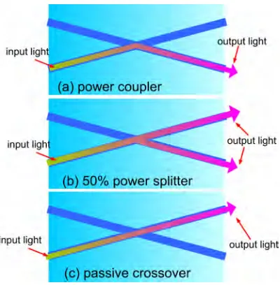
[image:27.595.219.419.462.666.2]The three main functions performed by X-couplers, namely as a power coupler, a 50:50 splitter or as a passive crossing, are depicted in Fig. 2.4. The arrows indicate the power flow from the input waveguide across the structure.
Figure 2.4 Schematic of three main functions of X-couplers: (a) power coupler; (b) 50% power
Perpendicular intersections between waveguides are common and are frequently employed due to their low crosstalk5. However, further increase in chip density could only be achieved if the intersection angles are made smaller [30, 31]. Work by Przyrembel et al [32] on crossed waveguides on a silica-on-silicon sample with 0.7% index difference found that the angles at which low crosstalk values (< -25dB) are attainable, are about a factor of 3 smaller (∼5º-8º) than the angles conventionally used (> 20º). The authors used 6µ m wide curved waveguides with 10mm curve radius. Modelling work by Agrawal et al [33] on a 2µm wide LiNbO3 waveguide having core and underclad refractive indices of 2.305 and
2.30 respectively also discovered that zero crosstalk occurs at intersecting angles of ~ 5º - 6º. It is also of interest to determine the angles at which near perfect (~100%) power coupling between the excited channel and the passive one can be achieved. This property would be of much use in the design of routing devices such as power couplers, optical add-drop multiplexers (OADM) and switches without the need for a finite interaction length, hence leading towards higher integration. Theoretical and experimental results on UV-written small angle X-couplers are presented in Chapters 5 and 6 respectively.
Another important waveguide structure is the planar Bragg grating, which is a periodic (spatial) perturbation of refractive index along a waveguide, usually along the plane that is orthogonal to the waveguide axis or signal direction [34, 35], as illustrated in Fig. 2.5.
Figure 2.5 Illustration of periodic refractive index perturbation in a channel waveguide, forming a
grating structure.
5
Crosstalk in this case is defined as the ratio between the coupled power and the total output power of
In general, a Bragg grating could be classified as a wavelength selective filter or reflector. It performs the function by coupling the incident mode (usually forward propagating mode) to other modes, whether backward propagating modes (reflection or short-period gratings) or forward propagating modes (transmission or long-period gratings). The coupled modes can be guided, cladding or radiation modes, depending on the design of the grating. A schematic of a reflection grating is shown in Fig. 2.6, illustrating a broadband signal (λbroad) being input into a channel inscribed with a grating structure. The output of the
[image:29.595.164.475.281.504.2]device is the broadband signal with a dip (λbroad - λBragg) centred at the Bragg wavelength.
Figure 2.6 Illustration of the operational properties of a reflection grating.
Numerous physical grating parameters can be varied in order to achieve a required spectral response. These include the strength of the induced index change, the length and period of the index perturbation, apodisation and fringe tilt. The types of Bragg gratings are usually determined by the variation of the induced refractive index change along the waveguide axis.
2.3
Summary
An overview of integrated optics has been presented covering the motivations and challenges faced by engineers in advancing the field. The description has highlighted the value chain of this technology and provided a few examples of integrated optics based solutions. A brief introduction to X-couplers and Bragg gratings, two of the devices that form an integral part of this thesis was also presented.
References:
[1] D. Marcuse, Integrated Optics, IEEE Press, New York, 1972.
[2] This was mentioned by G. Maxwell in his talk during the Centre of Integrated Photonics (CIP) Open Day in 2006. Graeme is currently CIP's Vice President of Hybrid Research & Development. His responsibility includes hybrid integration of active and passive components at CIP, including hybrid device design, planar silica fabrication and assembly of hybrid devices. He is a renowned authority on hybrid integration and PLC technology and was part of the management team that built up the business case to establish CIP.
For a full biography, see: http://www.ciphotonics.com/cip_people_GM.htm [3] G. Lifante, Integrated photonics: Fundamentals: Wiley, England 2003.
[4] Y. Hibino, H. Okazaki, Y. Hida, and Y. Ohmori, "Propagation loss characteristics of long silica-based optical waveguides on 5 inch Si wafers," Electronics Letters, vol. 29, pp. 1847-1848, 1993.
[5] N. Takato, K. Jinguji, M. Yasu, H. Toba, and M. Kiwachi, "Silica-based single-mode waveguides on silicon and their application to guided-wave optical interferometers," Journal of Lightwave Technology, vol. 6, pp. 1003-1010, 1988. [6] M. Svalgaard and M. Kristensen, "Directly UV-written silica-on-silicon planar
waveguides with low loss," Electronics Letters, vol. 33, pp. 861-863, 1997.
[7] L. Ming, "Fabrication and applications of zinc indiffused waveguides in periodically poled lithium niobate," PhD thesis, University of Southampton, 2005.
[8] L. Eldada and L. W. Shacklette, "Advances in polymer integrated optics," IEEE
Journal on Selected Topics in Quantum Electronics, vol. 6, pp. 54-68, 2000.
[9] DTI document entitled: "Photonics: A UK strategy for success," 2006. This can be obtained from:
http://www.dti.gov.uk/sectors/electronicsit/ukphotonicsstrategy/page30715.html [10] Y. Jaouen, L. du Mouza, D. Barbier, J.-M. Delavaux, and P. Bruno,
"Eight-wavelength Er-Yb doped amplifier: Combiner/splitter planar integrated module,"
IEEE Photonics Technology Letters, vol. 11, pp. 1105-1107, 1999.
[11] D. Barbier, M. Rattay, F. Saint Andre, G. Clauss, M. Trouillon, A. Kevorkian, J. M. P. Delavaux, and E. Murphy, "Amplifying four-wavelength combiner, based on erbium/ytterbium-doped waveguide amplifiers and integrated splitters," IEEE
Photonics Technology Letters, vol. 9, pp. 315-317, 1997.
[12] B. K. Das, R. Ricken, and W. Sohler, "Integrated optical distributed feedback laser with Ti:Fe:Er:LiNbO3 waveguide," Applied Physics Letters, vol. 82, pp. 1515-17,
[13] T. Tanaka, Y. Hibino, T. Hashimoto, M. Abe, R. Kasahara, and Y. Tohmori, "100-GHz spacing 8-channel light source integrated with external cavity lasers on planar lightwave circuit platform," Journal of Lightwave Technology, vol. 22, pp. 567-573, 2004.
[14] J. Hubner, S. Guldberg-Kjaer, M. Dyngaard, Y. Shen, C. L. Thomsen, S. Balslev, C. Jensen, D. Zauner, and T. Feuchter, "Planar Er- and Yb-doped amplifiers and lasers," Applied Physics B: Lasers and Optics, vol. 73, pp. 435-438, 2001.
[15] T. Mizuno, T. Kitoh, M. Itoh, T. Saida, T. Shibata, and Y. Hibino, "Optical spotsize converter using narrow laterally tapered waveguide for planar lightwave circuits,"
Journal of Lightwave Technology, vol. 22, pp. 833-839, 2004.
[16] M. Kohtoku, S. Oku, Y. Kadota, Y. Shibata, and Y. Yoshikuni, "Spotsize converters integrated with deep ridge waveguide structure," Electronics Letters, vol. 34, pp. 2403-2404, 1998.
[17] R. B. Swint, T. S. Yeoh, V. C. Elarde, J. J. Coleman, and M. S. Zediker, "Curved Waveguides for Spatial Mode Filters in Semiconductor Lasers," IEEE Photonics
Technology Letters, vol. 16, pp. 12-14, 2004.
[18] Y. P. Li, C. H. Henry, E. J. Laskowski, C. Y. Mak, and H. H. Yaffe, "Waveguide EDFA gain equalisation filter," Electronics Letters, vol. 31, pp. 2005-2006, 1995. [19] T. Tanaka, H. Takahashi, M. Oguma, T. Hashimoto, Y. Hibino, Y. Yamada, Y.
Itaya, J. Albert, and K. O. Hill, "Integrated external cavity laser composed of spot-size converted LD and UV-written grating in silica waveguide on Si," Electronics
Letters, vol. 32, pp. 1202-1203, 1996.
[20] S. Kawanishi, K. Hattori, H. Takara, M. Oguma, O. Kamatani, and Y. Hibino, "Actively modelocked ring laser using Er-doped silica-based planar waveguide amplifier," Electronics Letters, vol. 31, pp. 363-364, 1995.
[21] Biosensor Market, R&D and Commercial Implication www.fuji-keizai.com/e/report/ biosensor2004_e.html < 28th September 06>
[22] O. Boyraz and B. Jalali, "Demonstration of a silicon Raman laser," Optics Express, vol. 12, pp. 5269-5273, 2004.
[23] A. W. Fang, P. Hyundai, O. Cohen, R. Jones, M. J. Paniccia, and J. E. Bowers, "Electrically pumped hybrid AlGaInAs-silicon evanescent laser," Optics Express, vol. 14, pp. 9203-9210, 2006.
[24] H. Raether, Surface plasmons on smooth and rough surfaces and on gratings: Springer-Verlag, Germany, 1988.
converter (BEND SS-SOA)," Journal of Lightwave Technology, vol. 19, pp. 1745-1750, 2001.
[26] J. Salzman, H. Olesen, A. Moller-Larsen, O. Albrektsen, J. Hanberg, J. Norregaard, B. Jonsson, and B. Tromborg, "Distributed feedback lasers with an S-bent waveguide for high-power single-mode operation," IEEE Journal of Selected Topics
in Quantum Electronics, vol. 1, pp. 346-355, 1995.
[27] K. Takada, M. Oguma, H. Yamada, S. Mitachi, and M. Golling, "Gain distribution measurement of an erbium-doped silica-based waveguide amplifier using a complex OLCR," IEEE Photonics Technology Letters, vol. 9, pp. 1102-1103, 1997.
[28] S. Tomljenovic-Hanic and W. Krolikowski, "New design for a variable optical attenuator based on a bent channel waveguide," Applied Physics B: Lasers and
Optics, vol. 77, pp. 19-23, 2003.
[29] H. Hillmer, A. Grabmaier, S. Hansmann, H. L. Zhu, H. Burkhard, and K. Magari, "Tailored DFB laser properties by individually chirped gratings using bent waveguides," IEEE Journal of Selected Topics in Quantum Electronics, vol. 1, pp. 356-362, 1995.
[30] P. Gerard, P. Benech, and R. Rimet, "Intersecting waveguide modelization for any angle and guiding conditions with the radiation spectrum method," Optics
Communications, vol. 124, pp. 165-174, 1996.
[31] A. Neyer, W. Mevenkamp, L. Thylen, and B. Lagerstrom, "A beam propagation method analysis of active and passive waveguide crossings," Journal of Lightwave
Technology, vol. T-3, pp. 635-642, 1985.
[32] G. Przyrembel and B. Kuhlow, "Waveguide crossings with low crosstalk at small angles," Electronics Letters, vol. 38, pp. 1533-1535, 2002.
[33] N. Agrawal, L. McCaughan, and S. R. Seshadri, "A multiple scattering interaction analysis of intersecting waveguides," Journal of Applied Physics, vol. 62, pp. 2187-2193, 1987.
[34] K. O. Hill and G. Meltz, "Fiber Bragg grating technology fundamentals and overview," Journal of Lightwave Technology, vol. 15, pp. 1263-1276, 1997.
Chapter 3
Fabrication of Silica-Based Planar Waveguide
Devices
Following from the overview presented in Chapter 2, here we will discuss the various ways in which silica based waveguide devices are fabricated. The first question is: why does silica remain the material of choice when it comes to passive optical devices? The obvious reason is that it is the same material as optical fibres, making the two compatible in many respects. Secondly, silica samples are fabricated using techniques that were derived from the already mature micro-electronics industry, resulting in relatively inexpensive production costs. This is also part of the reason why silica planar samples are fabricated on silicon host substrates, leading to the name silica-on-silicon (SiO2:Si). In addition to their wide availability, silicon
wafers offer the advantages of a high degree of planarity, ready adhesion of deposited silica, have excellent heat dissipation properties and a high melting point (>1400ºC [1]) that enable them to withstand the levels of temperatures involved during deposition/consolidation of the glass layer [2, 3]. Their compatibility with microelectronics also means that they can be utilised as the optical bench on which to mount optoelectronic chips such as laser diodes and detectors, and then couple these to the silica waveguide ends [4]. Apart from silicon, fused silica wafers are also utilised as the host substrate. However, this tends to be a more expensive option as silica wafers are not mass produced. Another difficulty associated with silica host substrates is the problem of cracking due to differing thermal expansion coefficients between doped- and un-doped silica layers. This could result in low yields and would therefore add to the costs of developing such technology.
Absorption is a feature resulting from impurities in the silica matrix introduced during fabrication (extrinsic losses) and/or the inherent characteristics of the silica material itself (intrinsic losses). The term impurities in this case could imply either dopants added during the fabrication run to modify certain feature of the silica, or contaminants. An example of intrinsic losses is the infra-red absorption band of silica at λ > 1580nm (loss in excess of 1dB/km). However, this effect plays little role within the operating wavelengths of interest. Absorption due to OH ions dissolved in glass falls under extrinsic losses and these absorption peaks are at 720, 880, 950, 1130, 1240 and 1380nm [5], with peaks at 1240 and 1380 being the largest and most detrimental. For example, the loss due to 1ppm of OH impurity at 1380nm is ~ 4dB/km. Another form of loss is due to Rayleigh scattering which causes radiative losses, where guided light radiates into the cladding and is eventually lost. Rayleigh scattering results from inhomogeneities within the silica which are dimensionally smaller than the wavelength of light. Loss due to this type of scattering is proportional to λ-4 and decreases rapidly with increase in wavelength. In pure fused silica for example, scattering losses at 1300 and 1550nm were calculated to be 0.31dB/km and 0.15dB/km respectively [5]. In terms of layer uniformity, a planar substrate should display thickness variation and surface roughness of better than 0.1µm and 0.1nm respectively [6].
3-layer silica-on-silicon samples were utilised throughout this work. A schematic representation and image of the substrate are shown in Fig. 3.1. The typical refractive index value for the core layer is 1.45 with relative index difference, ∆ of 0.3%. Relative index difference in this case is defined as [2]:
−
=
∆
2 2 22
core clad coren
n
n
[3.1]where ncore and nclad are the core and cladding refractive index respectively. For weakly
guiding waveguides where ncore ≈ nclad, then ∆ is << 1 and the above expression can be
accurately approximated by:
Figure 3.2 Thin film deposition
process steps. In all steps,
process monitoring is essential.
Figure 3.1 Schematic and photo of a three layer silica-on-silicon sample.
3.1
Planar Deposition Techniques
Various aspects of planar sample thin film deposition are described here. Knowledge gained in these methods will also be useful in gauging the significance of the flat fibre work presented in Chapter 9. Donald L. Smith’s book on thin film deposition techniques [7] provides an excellent reference and is often quoted here. In general, all thin-film processes involve the sequential steps shown in Fig. 3.2.
A source of material is first provided. Then the material is transported to the target (a wafer or preform tube) where deposition takes place. Sometimes the film is subsequently annealed or consolidated, and finally it is analysed to evaluate the success of the process [7]. Thin film processes that employ solid source materials that are vaporised through heat or energetic beam of electrons, photons (laser ablation) or positive ions (sputtering) are categorised as physical vapour deposition (PVD). Those employing chemical means to convert solids to vapours, or supplies of source materials in the form of gas or evaporated liquids fall under the chemical vapour deposition (CVD) category.
established integrated microelectronics circuits industry. Low loss and reproducible waveguides are made by using techniques traditionally used for very large scale integrated circuits, usually based on multi-layer combinations of deposited silicon or silica. The most common deposition techniques are plasma enhanced chemical vapour deposition (PECVD) and flame hydrolysis deposition (FHD). PECVD and FHD are widely used in fabricating silica-on-silicon samples. In PECVD, a radio frequency (RF) discharge creates a low pressure plasma in an appropriate gas mixture that is used to initiate chemical reactions that produce silica layers. FHD involves the production of soot through the injection of halide1 reagents into a hydrogen/oxygen flame. Silica can be produced via either direct oxidation or hydrolysis, depending on the flame temperature. Other techniques that are employed in producing silica substrates, which are not categorised as deposition techniques, include thermal oxidation and sol-gel.
3.1.1 Thermal Oxidation
Thermal oxidation is probably the simplest technique for creating silica films by means of oxidising the surface of a silicon wafer [8]. The oxidation process is achieved by placing silicon wafers into a high temperature and high pressure oxygen or water vapour environment. Typical operating temperatures vary and are within the regions of 700 - 1000ºC. The deposition rate is a function of the substrate temperature, ambient pressure and reagent flow rate, with [8] reporting a rate of < 1µm/minute for phosphosilicate (SiO2-P2O5)
glass layers with a silicon substrate temperature below 1000ºC. The formed silica layer is also often referred to as thermal oxide or buffer layer. The disadvantages of this technique include difficulty in adding dopants into subsequent layers (core and overclad) [9] mainly due to the thermal gradient needed and the consumption of the available native silicon species on the surface of the host substrate, and also the advent of unwanted diffusion of dopant molecules between layers of different compositions of the sample [3]. As such, this technique is mainly used in fabricating the buffer layer for use as an underclad, serving to isolate the waveguides in the core layer from the high refractive index silicon layer, thus protecting from mode leakage into the high index silicon layer (silicon typically has a refractive index in excess of 3). For example, our samples that were purchased from the Centre of Integrated Photonics (CIP) have a thermal oxide underclad layer of 15.9µm. In
1 A halide consists of one part halogen atom and the other part an element or radical that is
addition to being utilised as the underclad layer, in some cases, the thermal oxide layer is used in conjunction with FHD (see below) i.e. the host substrate silicon has a thin thermal oxide layer so as to assist in FHD soot adhesion. This thin layer is typically about 5µm thick.
3.1.2 Sol Gel
[image:38.595.112.525.331.585.2]This technique is based on the synthesis of glass via solution chemistry. In this case glass is formed not directly at high temperatures from a melt, but at low temperatures (< 1200ºC) from suitable compounds by chemical polymerisation in a liquid phase [8]. In this way a gel is first formed from which glass may be obtained both by gradual removal of liquid and densification through thermal treatment (annealing/sintering). The main steps of sol gel processing are summarised in Fig. 3.3 [8].
Figure 3.3 Summary of sol gel processing (taken from [8]).
polymerisation. The glass is then baked at ~ 500ºC. Layers up to 3000Å can be fabricated via this approach in each cycle.
The main difficulty of this technique is preventing cracking of the layers as they dry [1, 8], particularly when forming glass films. This is a result of non-uniform shrinkage of the drying body, leading to stress. The drying stage also takes longer compared to the consolidation stage in other methods (such as FHD), with [8] stating that this could reach ‘hundreds of hours even for small specimens with surface areas of a few square centimetres’.
3.1.3 Plasma Enhanced Chemical Vapour Deposition
Plasma Enhanced Chemical Vapour Deposition (PECVD) was initially developed for the microelectronics industry. It utilises energy provided by RF or microwaves to dissociate the reactants, creating high energy plasma that would then facilitate thin film deposition. The main advantage of this technique is that depositions can be carried out at low temperatures due to the additional energy provided by the plasma. A schematic diagram of the PECVD deposition chamber and process is shown in Fig. 3.4.
Figure 3.4 PECVD deposition chamber and process schematic.
The chemical reactions taking place during PECVD are as follow [9]: a) when oxygen is used: SiH4 + O2 SiO2 + 2H2;
![Table 2.1 Materials technology for integrated optical devices [taken from [3]].](https://thumb-us.123doks.com/thumbv2/123dok_us/8488207.344135/21.595.108.531.322.566/table-materials-technology-integrated-optical-devices-taken.webp)
![Figure 3.3 Summary of sol gel processing (taken from [8]).](https://thumb-us.123doks.com/thumbv2/123dok_us/8488207.344135/38.595.112.525.331.585/figure-summary-sol-gel-processing-taken.webp)

![Table 3.1 Summary of effect of dopants relative to pure silica [22, 23].](https://thumb-us.123doks.com/thumbv2/123dok_us/8488207.344135/42.595.110.532.391.619/table-summary-effect-dopants-relative-pure-silica.webp)