Rochester Institute of Technology
RIT Scholar Works
Theses Thesis/Dissertation Collections
9-8-2006
A sub 1V bandgap reference circuit
Ashish Digvadekar
Follow this and additional works at:http://scholarworks.rit.edu/theses
This Thesis is brought to you for free and open access by the Thesis/Dissertation Collections at RIT Scholar Works. It has been accepted for inclusion in Theses by an authorized administrator of RIT Scholar Works. For more information, please [email protected].
Recommended Citation
A Sub 1 V Bandgap Reference Circuit
by
Ashish A Digvadekar
A Thesis submitted in Partial Fulfillment of the Requirements for the Degree of
MASTERS OF SCIENCE In
Electrical Engineering
Approved by: Professor _____________________________
(Dr. James E. Moon – Advisor)
Professor _____________________________
(Dr. P R Mukund – Committee Member)
Professor _____________________________ (Dr. Syed S. Islam – Committee Member)
Professor _____________________________
(Dr. Robert J. Bowman – Department Head)
DEPARTMENT OF ELECTRICAL ENGINEERING COLLEGE OF ENGINEERING
THESIS RELEASE PERMISSION
DEPARTMENT OF ELECTRICAL ENGINEERING
COLLEGE OF ENGINEERING
ROCHESTER INSTITUTE OF TECHNOLOGY
ROCHESTER, NEW YORK
Title of Thesis:
A Sub 1 V Bandgap Reference Circuit
I, Ashish Digvadekar, hereby grant permission to Wallace Memorial Library of the Rochester Institute of Technology to reproduce my thesis in whole or in part. Any reproduction will not be for commercial use or profit.
ACKNOWLEDGEMENT
A journey is easier when you travel together. Interdependence is certainly more valuable than independence. I have worked on this thesis for more than a year. I owe the completion of this thesis to a countless number of people. It is impossible to mention all the names here but I would definitely take this opportunity to thank the following people who have guided, encouraged, motivated and helped me through the different phases of the thesis.
First I would like to thank Dr. Moon for his valuable guidance throughout. He was always there to answer each of my doubts, from the trivial ones to the more genuine ones. The fruitful discussions with him were something I always looked forward to. He has also been of great help to me in matters not concerning the thesis. I have worked with him for two and a half years now and he inspired me both as a human being and as an advisor.
I would especially like to thank my boss and senior colleagues of the Temperature Sensor group at East Coast Labs of National Semiconductors for the knowledge they shared with me. Thank you Mr. Eric Blom and Mr. Gary Sheehan for introducing to me the concept of digital trimming. Thank you Jun, Stuart, Peter, and Matt for answering my endless questions.
My friends were of great help right through the thesis. First to mention is Ashish Vora who always made valuable suggestions which have affected the outcome of the thesis. I will thank Aakash, Vivek, Ajish and the rest for the constructive criticism.
ABSTRACT
This thesis proposes a novel technique for a low supply voltage temperature-independent reference voltage. With the scaling of supply voltages, the threshold voltages don’t scale proportionally and thus low supply reference circuits have replaced the conventional bandgap reference circuit. The first chapter of this work discusses the conventional bandgap references (The Widlar and Brokaw references). The terminology used in the bandgap world is introduced here. The second chapter investigates the existing low supply voltage reference circuits with their advantages and the limitations. A table discussing all the investigated circuits is provided towards the end of the chapter as a summary.
TABLE OF CONTENTS
Acknowledgement………...
i
Abstract……….
iii
Table of Contents……….
iv
List of Figures………..
vi
List of Tables………
viii
Introduction
____ __Chapter # 1
1
Introduction………...1
1.1.1 Zener Based Voltage Reference………
2
1.1.2 Bandgap Voltage Reference……….
4
1.1
Bandgap terminology………6
1.2
Classical Bandgap Circuits – Widlar and Brokaw……….8
1.3.1 Widlar Bandgap reference………
8
1.3.2 Brokaw Bandgap reference………..
10
1.4 Bandgap reference principle………
12
Background of Low Supply Voltage Bandgap Reference __ Chapter # 2
2.1 Background of Low Supply Voltage Bandgap Reference………. 142.2 Resistor Divider Network………. 16
2.3 Current Summing and a voltage summing Circuit….……….. 19
2.4 Transimpedance Amplifier……….. 22
2.5 Dynamic Threshold MOS (DTMOS)………... 24
2.6 Depletion transistors………. 26
2.7 Threshold Voltage based circuit……….. 28
2.8 Bandgap using two Vbe sources……….. 29
Proposed Low Supply Bandgap Reference Circuit __ Chapter # 3
3.1 Proposed Low supply Bandgap Reference circuit………... 34
3.2 Operation………. 37
3.2.1 PTAT Current Generation……… 37
3.2.2 CTAT Current Generation……… 41
3.3 CTAT Voltage Generation at the base of current mirror transistors………... 46
3.4 Bandgap output Voltage……… 49
Versions of the Bandgap Reference __ Chapter # 4
4.1 Versions of the Bandgap Reference………... 504.2 Circuit Variation # 1………... 53
4.3 Circuit Variation # 2………. 58
4.4 Comparison Chart………. 61
Process Variations and Transient Response __ Chapter # 5
5.1 Process Variations and Transient Response……….... 625.1.1 Process Variations……… 62
5.1.2 Transient Analysis………... 66
Conclusions and Future Work………..
68LIST OF FIGURES
1.1 Buried Zener reference circuit……….. 2
1.2 Basic Bandgap Circuit……….. 4
1.3 Widlar bandgap reference………. 8
1.4 Brokaw bandgap reference………... 10
1.5 a) Vertical NPN transistor b) Vertical PNP transistor……….. 12
1.6 Conventional BGR circuit………. 13
2.1 BGR using resistor divider network……… 16
2.2 Measured VREF characteristics of the proposed BGR……….. 17
2.3 Low voltage BGR as presented by [6]………. 18
2.4 Generated reference voltage vs temperature………. 18
2.5 Current Summing BGR………. 19
2.6 Temperature variation of the BGR in the current summing circuit………. 20
2.7 Voltage Summing BGR……… 21
2.8 a) VREF vs. Vdd b) VREF vs. Temperature……… 21
2.9 Transimpedance Amplifier using BGR………. 22
2.10 Measured VREF characteristics without trimming………... 23
2.11 DTMOS cross-section……….. 24
2.12 Low voltage DTMOS BGR……….. 25
2.13 VREF vs temperature………... 25
2.14 Opamp using transistors in depletion mode……….. 26
2.15 Simulated output voltages at 27ºC at different supply voltages………... 27
2.16 Measured VREF vs supply voltage for various temperatures………. 27
2.17 Threshold Voltage BGR Concept………. 28
2.18 Simulated BGR Output………. 28
2.19 Zero TC point……… 29
2.20 Low voltage bandgap using two Vbe sources……….. 30
2.21 Zero TC with two Vbe sources………. 30
2.22 Combining Vbe resistors………... 31
3.1 Proposed bandgap reference in the simplest form……… 35
3.2 Circuit for PTAT current generation………. 37
3.3 PTAT current……… 39
3.4 PTAT voltage drop across the output resistor……….. 40
3.7 Current through the resistor network……… 44
3.8 Voltage drop across output resistor due to the CTAT generation circuit…………. 45
3.9 Biasing Circuit……….. 46
3.10 Output from the biasing circuit………. 48
3.11 Bandgap output for a particular combination of resistors………. 49
4.1 Voltage supply variation of the basic BGR circuit………... 51
4.2 Circuit Variation # 1………. 54
4.3 Threshold voltage self biasing……….. 54
4.4 Supply voltage for the PTAT generating part of the circuit………. 56
4.5 Variation of output voltage with 100 mV supply voltage variation………. 56
4.6 Performance over temperature……….. 57
4.7 Circuit Variation # 2………...……….. 58
4.8 PSRR of Circuit Variation # 2……….. 59
4.9 Bandgap output voltage……… 60
5.1 The resistor and transistor trim configuration for the original circuit………. 64
5.2 Transient response of the original circuit……….. 66
5.3 Transient response for Circuit Variation # 1………. 67
5.4 Transient response for Circuit Variation # 2………. 67
LIST OF TABLES
1.1 Introduction
1.1.1 Zener Based Voltage Reference 1.1.2 Bandgap Voltage Reference 1.2 Bandgap terminology
1.3 Classical Bandgap Circuits – Widlar and Brokaw 1.3.1 Widlar Bandgap reference 1.3.2 Brokaw Bandgap reference 1.4 Bandgap reference principle
_________________________________
1.1 - INTRODUCTION
Some of the desired characteristics of a voltage reference are:- a) Ability to be implemented in silicon.
b) Accuracy and stability over supply voltage & time. c) Proper startup value.
d) Accurate over a wide range of temperature.
The two most popular voltage references are:- a) Zener-based Voltage reference
b) Bandgap Voltage reference
1.1.1 Zener-based voltage reference
The simplest and the conventional form of a voltage reference is the Zener-based voltage reference. Here the Zener diode operates in the reverse bias region and current begins to flow in it at a specific voltage (around 6 V) and thereafter the current increases rapidly with the increase in voltage. Thus, to use it as a reference a constant current is required. This is provided through a resistor from a higher supply voltage.
Figure 1.1 [12] shows a buried Zener voltage reference where the diode is biased by a current source. The resistors R1 and R2 form a resistor divider network across the Zener diode. The divided voltage is applied to the non-inverting terminal of an operational amplifier whose output is the reference voltage. The gain of the amplifier is decided by the resistor values R4 and R3. The expression for the output is
(
R R)
V RR R
Vout + ×
+
= 1 4 3 2
1
2 (1.1)
They are called buried diodes as they are fabricated beneath the surface of the chip. The ones fabricated on the surface are noisier as they can get contaminated easily. The buried diode references are more expensive than the bandgap references but are more accurate. Buried Zener diodes can be made with a range of voltages and have good low noise performance (better than bandgap references), but the ones that, in combination with their temperature compensating diodes, have a breakdown voltage just below 7 V, have the best temperature performance.
1.1.2Bandgap Voltage Reference
A Bandgap reference circuit is one where two quantities with opposite temperature coefficients are added with a proper weighing factor to result in a temperature coefficient of approximately zero. This can be explained as two quantities B1 and B2 having opposite
temperature coefficients and choosing the coefficients c1 and c2 in such a way that
2 0
2 1
1 ∂ =
∂ + ∂ ∂
T B c T B
c (1.2)
[image:15.612.197.434.335.625.2]Thus the reference voltage Vout = c1V1+c2V2 has a zero temperature coefficient.
Figure 1.2 shows a bandgap circuit in its very basic form. Here the Vbe, which has a negative
temperature coefficient is complementary to absolute temperature and the delta Vbe is
proportional to absolute temperature and a weighted addition of both results in the Vref with a
1.2 - BANDGAP TERMINOLOGY
a) Bandgap Voltage
Bandgap voltage of a semiconductor measured in eV refers to the potential energy difference between the valence band and the conduction band for that semiconductor. It has a nearly constant value and its variation with temperature is small. Each type of a semiconductor has a unique bandgap. Typically for silicon its value is approximately 1.17 eV.
b) PTAT Voltage
PTAT stands for proportional to absolute temperature which means that the quantity varies proportionally with absolute temperature - i.e., the quantity increases with absolute temperature. Most of the bandgap reference circuits use the difference in the Vbe’s of two
transistors operating under same current densities as the PTAT voltage.
c) CTAT Voltage
CTAT stands for complementary to absolute temperature which means that the quantity varies complementary to absolute temperature - i.e., the voltage decreases with absolute temperature. Most of the bandgap reference circuits because of its linearity use the Vbe of a
d) Bandgap Reference circuit (BGR)
A bandgap reference circuit is one which does a weighted addition on the PTAT voltage with the CTAT voltage to have an end result having a near-zero temperature coefficient. This resulting voltage is equal to the bandgap voltage of the semiconductor at the reference temperature.
e) Parts per million (PPM)
Reference-accuracy unit used commonly with precision voltage reference designs. Designers typically use this measure to specify temperature coefficients and other parameters
that change little under varying conditions. For a 2.5 V reference, 1 ppm is one-millionth of 2.5 V, or 2.5 µV. If the reference is accurate to within 10 ppm, then it is extremely good performance for any voltage reference.
f) Power Supply Rejection Ratio (PSRR)
PSRR is defined as the ability of the circuit to maintain its output voltage as its power-supply voltage is varied. The PSRR for a Bandgap reference circuit can be calculated by the equation
∆ ∆ =
− −
OUTPUT BANDGAP
SUPPLY POWER
V V
1.3 - CLASSICAL BANDGAP CIRCUITS – WIDLAR AND BROKAW
1.3.1 Widlar Bandgap reference
[image:19.612.190.442.365.666.2]The first bandgap reference was proposed by Robert Widlar in 1971 [2] as shown in Figure 1.3 below. It used conventional junction isolated bipolar technology to make a stable low voltage (1.220 V) reference. Early MOS implementations of these voltage references were based on the difference between the threshold voltages of enhancement and depletion mode MOS transistors [3]. This provides low temperature coefficient (TC); however, the drawbacks are that the output is not easy to control because of the direct dependence on the doses of ion implantation steps and, further depletion mode transistors are not available in most CMOS processes.
The Widlar circuit shown above operates as explained with equations below:
VBE3 =VBE4 +I2R3
(1.4)
∴VBE3−VBE4 =I2R3 ∆VBE =I2R3 (1.5)
But, ∆ = − = 1 2 2 1 2 2 1
1 ln ln
ln S S Thermal S Thermal S hermalT BE I I I I V I I V I I V
V (1.6)
Assuming that Vbe3 = Vbe2, this implies I1R1=I2R2
∴ = ∆ = = 1 1 2 2 3 1 2 2 1 3 3
2 ln ln
S S Thermal S S Thermal BE I R I R R V I I I I R V R V
I (1.7)
2 2 1 1 2 2 3 2 2 2
2 ln BE Thermal BE
S S Thermal
BE
OUT V KV V
I R I R V R R V R I
V = + = + = +
∴ (1.8)
R1, R2 and R3 can be manipulated to achieve the desired value of K.
1.3.2 Brokaw Bandgap reference
Paul Brokaw made his bandgap reference [13] by solving many of the problems in the Widlar reference. Figure 1.4 below shows the Brokaw bandgap reference circuit. The circuit has two transistors and collector current sensing to form the basic bandgap voltage. The output voltage can be expressed as
VOUT =VBE1 +Voltage_across_R1 (1.9)
∴ = +
2 1 2
1
1 2 ln A
A q kT R R V
VOUT BE (1.10)
Here A1 and A2 are the areas of Q1 and Q2 respectively.
The reason for the voltage across R1 having a positive temperature coefficient is that the
currents through both the transistors are equal, thus acts like a PTAT. The Vbe acts as a
1.4
- BANDGAP REFERENCE PRINCIPLE
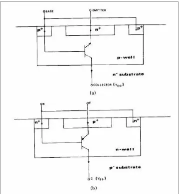
[image:23.612.136.497.239.629.2]Most of the modern bandgap reference circuits are made on the Paul Brokaw school of thought. Thus every bandgap reference will result from the weighted addition of a PTAT voltage with a CTAT voltage. For this they rely on well transistors. These are vertical bipolar transistors that use wells as their bases and substrate as their collectors. These are shown in Figure 1.5 below.
A conventional bandgap [4] reference circuit is shown in the Figure 1.6. The output of the circuit is given by the equation:
(
)
3 2 3 2 R R R V VVOUT BE BE
+ ∆
+
= (1.11)
∴ = + +
3 2 2 ln 1 R
R n V V
VOUT BE t (1.12)
Here n is the ratio of the sizes of the two bipolar junction transistors and Vt is the thermal
[image:24.612.196.434.334.536.2]voltage. The first term represents the CTAT voltage and the second term represents the PTAT voltage.
Figure 1.6 – Conventional BGR circuit [4]
2.1 Background of Low Supply Voltage Bandgap Reference 2.2 Resistor Divider Network
2.3 Current Summing and a voltage summing Circuits 2.4 Transimpedance Amplifier
2.5 Dynamic Threshold MOS (DTMOS) 2.6 Depletion transistors
2.7 Threshold Voltage based circuit 2.8 Low Voltage BGR Comparison
_________________________________
2.1 - BACKGROUND OF LOW SUPPLY VOLTAGE BANDGAP
REFERENCES
1) Resistive divider networks
2) Current summing and a voltage summing circuits 3) Transimpedance amplifier
4) Dynamic Threshold MOS (DTMOS) 5) Depletion transistors
2.2 RESISTOR DIVIDER NETWORK
The resistive divider network proposed by Banba [5] is shown in the Figure 2.1. The concept here used was to sum two currents (instead of voltages in the conventional BGR circuits). The forward bias voltage of the diodes is defined as VF. One of the currents is proportional to
VF, which is the CTAT here, and the other current in proportional to VT. The circuit
[image:27.612.135.494.324.545.2]configuration is shown in Figure 2.1 below. Here the diodes can be replaced with PNP transistors available in the today’s processes.
Figure 2.1 – BGR using Resistor divider network [5]
Here,
= +
3 2
1 4
R dV R
V R
V F F
REF (2.1)
The circuit was designed for a reference voltage of 515 mV. VREF showed a variation of 515
mV ± 1 mV for the supply variation of 2.2 to 4 V at 27°C; and 515 mV ± 3 mV for temperature variation from 27 to 125°C as shown in Figure 2.2 below. However the minimum supply voltage was limited to 2.1 V.
Figure – 2.2 Measured VREF characteristics of the proposed BGR [5]
Figure 2.3 – Low Voltage BGR as presented by [6]
The voltage at the nodes Va and Vb is now 150 mV – 200 mV due to the resistive divider network of R1a, R1b, R2a and R2b. The output impedance of the current source is improved by
[image:29.612.91.541.69.298.2]using cascade configuration. This also helps to maximize the PSRR of the circuit. The simulation results are shown in Figure 2.4. The TC variation was observed to be less than 0.24%.
Figure 2.4 – Generated reference voltage versus temperature using a 0.95 V (solid curve)
2.3 CURRENT SUMMING AND A VOLTAGE SUMMING CIRCUITS
Ripamonti [7] talks about two different configurations capable of sub-1 V supply voltage BGR circuits. The first technique operates by summing two currents with opposite temperature dependence on a resistor, and the resistor value further controls the reference voltage. The second technique sums two voltages that are first attenuated, where resistive voltage dividers are used for the determination of the attenuation factor. The circuit that sums two currents is given in Figure 2.5.
Figure 2.5 – Current Summing BGR [7]
The circuit is divided into three sub-blocks. The first generates current PTAT by using the MOS operating in the sub threshold region. The second block produces current CTAT. The third block is a resistor where both the currents are added. The major advantage of the circuit is that the supply voltage here is the addition of the drop across the forward biased diode and the VDS of the transistor, which are 0.7 V and 0.2 V respectively. Thus the supply voltage can
Figure 2.6 – Temperature Variation of the BGR in the current summing circuit [7]
The voltage summing BGR in Figure 2.7 is also composed of three sub circuits. The only difference between the current summing BGR and the voltage summing BGR is the third sub-circuit. The third section is composed of a differential amplifier in a non-inverting feedback loop. The offset voltage from the use of unmatched bipolar transistors generates the PTAT component. The applied diode voltage is not the full base-emitter voltage, as in a standard BGR, but a fraction. The minimum supply voltage of one path is VT plus a VCEsat,
plus the source to drain voltage of the current source. The second path’s minimum supply voltage is a VBE plus the minimum voltage of the current source plus the output voltage of
Figure 2.7 – Voltage Summing BGR [7]
Variations in reference voltage with supply voltage and temperature are plotted in Figure 2.8. The output voltage was found to vary by less than 0.5% over the 0.9 V to 2.5 V range. In the same range the temperature dependence varied by 2%.
2.4 TRANSIMPEDANCE AMPLIFIER
The conventional BGR circuit is limited by the input common mode range of the operational amplifier. Jiang [8] proposes another improvement to the circuit described by Banba [5], as depicted in Figure 2.9. Here resistors are used in place of input differential stage of the opamp. They are used to obtain a PTAT current by sensing the voltage difference and the current is summed with a current complementary to VEB to obtain the reference voltage. This
technique is based on the use of a Transimpedance amplifier.
Figure 2.9 – Transimpedance Amplifier using BGR [8]
The value of VREF here is given by
= + − 2 2 2 1 1 3 ln 1 R V R V A A V R R
V BE B
T
REF (2.2)
Here A1 and A2 are the areas of transistors Q1 and Q2 respectively. The value of Vref can be
2.5 DYNAMIC THRESHOLD MOS (DTMOS)
Annema [9] talks about another method of low power, low voltage BGR design through the use of dynamic threshold MOS (DTMOS) devices. As we have seen, the bandgap for low power applications can be made to appear smaller through resistive subdivision, but it is at the expense of area. The bandgap can also be made to appear smaller if the junction is in the presence of an electrostatic field. The electrostatic field lowers the bandgap. This method can be implemented by replacing the normal diodes with MOS diodes that have interconnected gates and back gates. These devices are DTMOS devices; a cross-section is shown in Figure 2.11. The use of a P-DTMOS device results in a VG0 of 0.6 V and the temperature gradient of
VGS is approximately –1 mV/°K. These values are half the typical values of a standard BGR.
Figure 2.11 – DTMOS Cross-section [9]
supply voltages. The opamp’s output stage, shaded, uses a low voltage current mirror. Correct operation of this opamp was verified for supply voltages down to 0.7 V.
Figure 2.12 – Low Voltage DTMOS BGR [9]
The circuit’s temperature dependence is shown in Figure 2.13. The variation over the range, -20°C to 100°C, is just 4.5 mV.
2.6 DEPLETION TRANSISTORS
Pierazzi [10] made opamp that used PMOS in the depletion mode in order to cope with the supply voltage reduction. Thus the circuit cannot be fabricated in regular low cost CMOS technologies that usually do not have these special devices. This opamp uses PMOS in the weak inversion and is shown in Figure 2.14. A diode-connected PMOS transistor loads the second gain stage. Thus, the biasing of the opamp is derived from the output voltage and thus this maximizes the PSRR of the whole opamp but at the cost of low voltage gain.
Figure 2.14 – OpAmp using transistors in depletion mode [10]
Figure 2.15 - Simulated output voltages at 27ºC at different supply voltages. BG1 is the curve
of our interest. [10]
The BGR was implemented in 0.35 µm CMOS technology. The measured VREF vs supply voltage for various temperatures is shown in Figure 2.16. The measurements suggest a minimum supply voltage of 0.9 V.
2.7 THRESHOLD VOLTAGE BASED CIRCUIT
Ytterdal [11] introduces the new concept of threshold voltage based voltage references. The basic idea here is to compensate the temperature dependency of the threshold voltage of a PMOS transistor with that of an NMOS transistor, both having a CTAT dependency. This concept is pictorially shown in Figure 2.17. The performance of the proposed BGR is shown to be comparable to bandgap circuits, but at the cost of more area and complexity.
Figure – 2.17 Threshold Voltage BGR Concept [11]
The simulation results for the circuit made with this technique are shown in Figure 2.18.
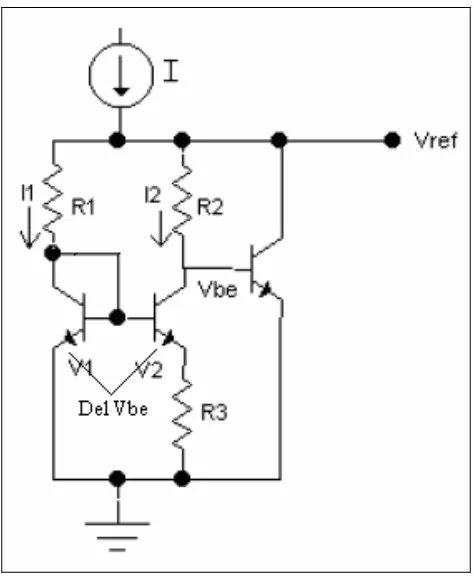
2.8 BANDGAP USING TWO VBE SOURCES
The work by Washburn [17] was driven by the motivation of developing a low voltage bandgap reference circuit having low power consumption, no dependence on TC of resistors, minimum number of critical components that need to be matched and usage of resistor arrays that are a multiple of a single resistance value.
The work in [17] exhibits a series of attainable circuit behaviors as discussed below:
a) The ability to multiply PTAT voltage to get it to be almost equal to the CTAT voltage near the center of the desired operating temperature range.
b) The voltage source like behavior of the multiplied PTAT voltage when dropped across a resistor having a impedance equal to that of the resistor value.
c) If CTAT and PTAT voltages are connected as shown in Figure 2.19 then the value of the resistor on the CTAT side can be chosen in a way to have near zero TC at the junction of the two resistors.
Figure 2.19 - Zero TC point [17]
d) The using of two equal resistors meeting at Vbg to generate a stiff Vbe voltage source as
Figure 2.20 – Low voltage bandgap using two Vbe sources [17]
The resulting output voltage is Vbg = 0.6 to 0.7 V depending upon the point of cancellation.
The Vbe (CTAT voltage) does not impose a limit on the voltage headroom. The headroom is limited by the mirrors. So according to [17] the minimum supply voltage depends upon the headroom needed for the mirrors to operate which is around 0.1 V in 90 nm technologies. So the supply voltage required is just above the output voltage Vbg.
[17] proposes a new resistor scheme where the resistors will be in the form of series and parallel stripes of a single resistor as shown conceptually in Figure 2.22 below.
Figure 2.22 - Combining Vbe Resistors [17]
2.9
LOW VOLTAGE BGR COMPARISON
The work done on low supply voltage bandgap references was discussed in this chapter. All of them have their own advantages and drawbacks. Table 1 below compares the results from all the discussed works. This gives an overall idea on the performance of the individual circuit compared to the others in areas like technology used, minimum supply voltage, output voltage, ppm accuracy and the PSRR in dB.
Circuit type Technology Min. Supply
Voltage (V) Output Voltage (V) Accuracy (ppm/ºC) PSRR (dB) Resistor Divider (Banba) 0.4 µm
CMOS 2.1 V 515 mV ±59 ppm/ºC
Not Mentioned
Resistor Divider
(Waltari) 0.6 m
CMOS 0.95 V 720 mV
.24%. Not mentioned in ppm. 44dB at 10KHz Current Summing (Ripamonti) Not
Mentioned 0.9V 521mv
2.4%. Not Mentioned in ppm. Low Transimpedance Amplifier (Jiang) 1.2 m
CMOS 1.2 V 1000 mV
+/- 100 ppm/˚C 20dB at 1KHZ DTMOS (Annema) 0.35 m CMOS
Depletion
Transistors
(Peirazzi)
0.35µm
CMOS 0.9 V 510 mV
Not Mentioned
Not Mentioned
Threshold
Voltage Based
(Ytterdal)
0.13 µm Digital CMOS
0.55 V 400 mV 93 ppm/ºC Not Mentioned
3.1 Proposed Low supply Bandgap Reference circuit 3.2 Operation
3.2.1 PTAT Current Generation 3.2.2 CTAT Current Generation
3.3 CTAT Voltage Generation at the base of current mirror transistors 3.4 Bandgap output Voltage
_________________________________
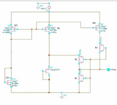
3.1 PROPOSED LOW SUPPLY BANDGAP REFERENCE CIRCUIT
Figure 3.1 - Proposed bandgap reference in the simplest form
Briefly, the working of the circuit can be explained as the summation of two currents (one PTAT and the other CTAT) across the resistor R3. The diode-connected BJT makes a
conventional CTAT current flow through the resistor combination R2 and R3. The two diode
connected transistors M3 and M4 are used for biasing. The voltage at the gate of the
transistors in the current mirror is of CTAT type. This voltage at the gate of M2 and the
The circuit is designed using the LSI Logic 0.18 micron CMOS process. The parametric values of the various components used in the circuit are mentioned in Table 2 below. Here the resistors used are all different from each other. R1 is P+ Poly resistor with a negative
temperature coefficient. R2 is a P+ Poly Silicided resistor with a positive temperature
coefficient and R3 is a Metal 1 resistor with a positive temperature coefficient.
Sr. # Part # Type Value
1 M1 PMOS W = 45 µm, L = 270 nm
2 M2 PMOS W = 1 µm, L = 180 nm
3 M3 PMOS W = 900 nm, L = 180 nm
4 M4 NMOS W = 8 µm, L = 180 nm
5 R1 P+ Poly Resistor 29.4 K
6 R2 P+ Ploy Silicided resistor 16.92 K
[image:47.612.85.547.235.474.2]7 R3 Metal 1 Resistor 7.46 K
3.2 OPERATION
The operation of the circuit will be studied by dividing it into three simpler parts. The first part will explain the generation of the PTAT current and the second will explain the generation of the CTAT current. The third will explain the PTAT nature of the gate voltage of the current mirror transistors M1 & M2.
3.2.1 PTAT Current Generation
The most conventional way of making the PTAT quantity is using the difference in the Vbe’s
of two PN junctions having different current densities. But this technique needs an operational amplifier to magnify the slope of the delta Vbe. Here, a new technique is used to
get the PTAT current.
[image:48.612.258.371.431.687.2]In the figure above the current in the resistors is given by the square law equation
'
(
)
22 1
T GS p
D L V V
W K
I = − (3.1)
where Kp = µ0COX for the transistor M2 & VT is the threshold voltage of the transistor.
D
(
VGS VT VGSVT)
LW Kp
I 2
2
1 2 + 2 −
=
∴ (3.2)
(
)
(
+ −)
∂ ∂ + − + ∂ ∂ = ∂ ∂∴ D OX GS T GS T VGS VT VGSVT
T V V V V T C L W T I 2 2 2
1 2 2
0 2
2
0
µ
µ
(3.3)
(
)
(
)
∂ ∂ − ∂ ∂ − + − + ∂ ∂ = ∂ ∂ ∴ T V T V V V V V V V T C L W TI GS T
T GS T GS T GS OX D 0 2 2
0 2 2
2
1
µ
µ
(3.4)
In the above equation (4), there are three parameters that will decide the nature of the current
versus temperature. They are 0 , & .
T V T V T T GS ∂ ∂ ∂ ∂ ∂ ∂µ
µ0 is the mobility of the carriers. Temperature appears explicitly in the value of surface
mobility for the MOSFET model. The temperature dependence for the mobility as explained in [14] is determined by:
( )
( )
1.50 0 0 0 = T T T T
µ
µ
(3.5)T VGS
∂ ∂
has a slope of around 393.09 µV/°C. This would be derived in a later section.
T VT
∂ ∂
here has a slope of about -65 µV/°C as seen from simulation results for this specific
transistor size and similar biasing. Thus the value of
∂ ∂ − ∂ ∂
T V T
VGS T
is around 460 µV/°C and
has a PTAT nature.
The variation of mobility with temperature is much smaller when compared to that of (VGS
-VT) and thus the current has a PTAT nature. The variation of the current and output PTAT
[image:50.612.142.489.405.607.2]voltage across temperature is shown in Figures 3.3 and 3.4 below.
3.2.2 CTAT Current Generation
The most conventional technique for generating the CTAT (voltage/current) is through the use of Vbe of the BJT.
Here the Vbe of the vertical PNP that is present in the technology is used. The variation of the
Vbe of theVPNP BJT with respect to temperature is shown in Figure 3.5 below. As seen from
the Figure 3.5, the voltage varies about 253.625 mV for the temperature range of -20°C to 120°C at a slope of -1.812 mV/°C.
Figure 3.5 – Variation of PN junction voltage with temperature
This variation is too large compared to that of the PTAT current across the output resistor R3.
This is reduced in its value by allowing a PTAT VGS for the current mirror transistor M1. This
The circuit generating the CTAT quantity is shown in Figure 3.6 below.
Figure 3.6 – Circuit generating CTAT quantity
Neglecting the base current for the BJT we have,
=
S BJT thermal
BE
I I V
V ln (3.6)
where Vthermal is the thermal voltage and IS is the saturation current which can be related to
the device structure by
i n i n B
n i
S Q Bn D B n T
D qAn
I = 2 = 2 = '2
µ
(3.7)Here ni is the intrinsic minority carrier concentration, QB is the total base doping per unit
area, µn is the average electron mobility in the base, A is the emitter base junction area and T
The quantities that are temperature dependent are given by − = = − thermal G i n n V V DT n CT 0 3 2 exp
µ
(3.8)Here VG0 is the bandgap voltage of silicon extrapolated to 0°K and the value of n is
approximately 1.5 as shown in equation (3.5).
C and D are temperature-independent quantities. Combining the above four equations yields
= − thermal G BJT thermal BE V V E T I V
V ln γ exp 0 (3.9)
E is another temperature independent constant and = 4 – n 2.5.
For our circuit, the current IBJT varies with temperature. We assume for the time being that
the temperature variation is known and that it can be written in the form
IBJT =GTα (3.10) Here G is another temperature-independent constant.
VBE =VG0 −Vthermal
[
(
γ
−α
)
lnT −ln( )
EG]
(3.11)In the above equation VG0, E & G are temperature independent quantities.
[
(
)
( )
]
(
)
(
)
( )
EG( – ) has a value of approximately -2.
T Vthermal
∂ ∂
can be calculated as shown below.
q kT
Vthermal = (3.13)
Here k is Boltzmann's constant, T is absolute temperature and q is electronic charge. Thus we have, q k q kT T T
Vthermal =
∂ ∂ = ∂ ∂
= 8.62 x 10⁻⁵ V/°K. (3.14)
Thus the resulting value of
T VBE
∂ ∂
is CTAT in nature. The value of the Vbe drop across the
output resistor R3 across temperature is shown in Figure 3.7 below. This slope of Vbe is
Figure 3.7 below shows the current through the resistor network
Figure 3.7 – Current through the resistor network
[image:56.612.149.483.457.669.2]3.3
CTAT VOLTAGE GENERATION AT THE BASE OF CURRENT
MIRROR TRANSISTORS
The CTAT voltage (i.e., the PTAT Vgs for PMOS) is generated by the biasing circuit which
consists of two diode-connected transistors M3 and M4. The biasing circuit is shown in
[image:57.612.238.392.243.642.2]Figure 3.9 below.
The output here can be given as mn mp mn DD OUT g g g V V 1 1 1 + ×
= (3.15)
where gmp and gmn are tranconductances of the PMOS and the NMOS transistors
respectively. mn mp mp DD OUT g g
g V V
+ =
∴ . (3.16)
(
)
∂ ∂ + ∂ ∂ × + − + × ∂ ∂ = ∂ ∂ ∴ T g T g g g g g g T g V TV mp mn
mn mp mp mn mp mp DD OUT 2 1 (3.17)
For the sake of derivation we will assume that
∂ ∂ = ∂ ∂ = ∂ ∂ T g T g T
gmp mn m
.
(
)
m(
mn mp)
mnmp DD
OUT g g
T g g g V T
V × −
∂ ∂ × + = ∂ ∂
∴ 2 (3.18)
In the above equation the two terms that will decide the nature of the output are
(
mp mn)
.m and g g
T
g −
∂ ∂
Here, gmn > gmp as the transconductance for NMOS is greater than PMOS if they are similarly
sized. Here, since NMOS is much larger than PMOS we surely have gmn > gmp.
The transconductance can be calculated as
D m V I g ∂ ∂
Temperature dependency of gm can be defined as
gm
( ) ( )
T =k T ×(
VGS −VT( )
T)
. (3.20) As discussed earlier both Vth and k decrease with the rise in temperature. But the effect of k(T) is more than that of Vth (T). Thus the overall value of gm reduces with the increase in
temperature. This change in gm is more than that of (gmn – gmp), and thus the output is of
CTAT in nature.
[image:59.612.140.491.323.535.2]The variation of the output with respect to temperature is shown in Figure 3.10 below
3.4 BANDGAP OUTPUT
The output of the circuit can be calculated by using the current in the two branches. If we assume the currents in the two branches to be I1 and I2 then the voltage Vout can be defined as
VOUT =
(
I1+I2)
R3 (3.21)2 3 2
1
R I R R
V
V BE
OUT = + +
∴ (3.22)
Using the above relation a desired value for Vout can be obtained by iterating the values of
[image:60.612.126.507.324.553.2]R1, R2 and R3. The output of a particular configuration of the resistors is shown in the
Figure 3.11 below.
Figure 3.11 - Bandgap output for a particular combination of resistors
4.1 Versions of the Bandgap Reference 4.2 Circuit Variation # 1
4.3 Circuit Variation # 2 4.4 Comparison Chart
_________________________________
4.1 VERSIONS OF THE BANDGAP REFERENCE
Figure 4.1 – Voltage supply variation of the basic BGR circuit
The PSRR of the circuit can be calculated by the equation
∆ ∆ =
− −
OUTPUT BANDGAP
SUPPLY POWER
V V
PSRR 20log in dB (4.1)
db mV
mV
PSRR 7.5191
077 . 42
100 log
20 =
= (4.2)
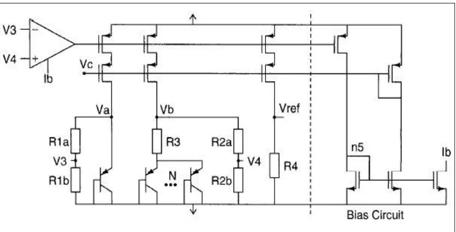
4.2 - CIRCUIT VARIATION # 1
[image:64.612.97.537.317.674.2]The biasing method used here as shown in Figure 4.3 is known as threshold voltage self biasing. The idea here is to get the current in the transistor M5 to be almost independent of supply voltage variations. This would make the voltage drop across the resistor R4 to be independent of supply voltage and will thus depend only on temperature.
Figure 4.3 – Threshold voltage self biasing
If we neglect the body effects and the channel length modulation effects then we can define the drop across the resistor as
(
)
R V R V I C L W I V VV GS THN
R OX R THN
GS
R = = + 4 = 8 ≈
5 4 8 4 / 2
This result implies that current IR4 will be independent of supply voltage. In practice, this is
not true due to the finite output resistance of the MOSFET’s.
The accuracy of current IR4 is determined by the threshold voltage accuracy and the resistor
accuracy, which could vary 20%. Note also that threshold voltage’s TCand the resistor’s TC determine the circuit’s temperature dependency. The temperature coefficient of the resistor is positive while that of the threshold voltage is negative.
Consequently, the threshold voltage self-biasing technique provides a current with a large negative temperature coefficient. This in the original circuit was done by the two diode connected transistors making up the biasing circuit. The CTAT nature of this voltage is very important to the functionality of the circuit as explained in the previous section.
The startup of the bias circuit is taken care of by the transistor M9 to avoid the zero current initial condition. The PTAT generating PMOS is provided with a power supply by a point on the bias circuit shown as the “Dummy Supply”. The characteristic needed in the supply is that it should vary very little with temperature and with actual supply voltage variation. But in this case the supply voltage has a PTAT nature as shown in Figure 4.4 below.
Figure 4.4 – Supply Voltage for the PTAT generating part of the circuit
This PTAT nature of the supply voltage results in a PTAT VGS for the transistor. This PTAT
VGS generates a PTAT current as explained in the previous chapter. The variation of this
voltage over 100 mV supply voltage variation is about 50 mV and thus the circuit exhibits a better PSRR compared to the original circuit.
[image:67.612.105.527.430.665.2]The PSRR of the circuit can be calculated by the equation ∆ ∆ = − − OUTPUT BANDGAP SUPPLY POWER V V
PSRR 20log in dB (4.4)
db mV
mV
PSRR 8.5269
4672 . 37 100 log 20 =
= (4.5)
[image:68.612.92.528.446.682.2]4.3 - CIRCUIT VARIATION # 2
[image:69.612.94.569.211.659.2]This variation of the circuit offers a significantly improved PSRR compared to the other two variations. This improvement in PSRR comes at the cost of lack of range in the output for the bandgap reference circuit. The circuit configuration is shown in Figure 4.7 below.
This variation of the original circuit is essentially the same as the first one. The only difference is that the PTAT generation circuit here uses a NMOS transistor in the source follower configuration. The advantage of this circuit is that the PSRR is very good but the major disadvantage of this configuration is the range of the output voltage. It is only usable up to 250 mV.
[image:70.612.93.542.292.509.2]Figure 4.8 below shows the output voltage over supply voltage variation of 100 mV.
Figure 4.8 - PSRR of Circuit Variation # 2
The PSRR of the circuit can be calculated by the equation
∆ ∆ =
− −
OUTPUT BANDGAP
SUPPLY POWER
V V
PSRR 20log in dB (4.6)
The PSRR of 27.2 dB is very good for a bandgap reference circuit. The other advantage of the circuit is the accuracy over temperature of about 38 ppm/ºC. The TC cancellation for this configuration is better than that in circuit variation #1. The variation of the bandgap output voltage over the temperature range of -20 °C to 80 °C is shown in Figure 4.9 below. The current consumed by this configuration was 110 µA.
4.4 - COMPARISON CHART
Table 3 below shows a parametric comparison between the three variations of the bandgap circuit to a good bandgap reference circuit. The good bandgap reference circuit considered here is the one by Banba [5]. As seen from the table every configuration has its own advantages and disadvantages when compared to each other or to the good bandgap reference circuit.
Parameter Proposed Circuit
Circuit
Variation –I
Circuit
Variation - II
Popular BGR
Circuit
Bandgap Output
Voltage 302 mV 460 mV 155 mV 515 mV
Output Voltage Range
200 mV to 600
mV 200 mV to 500 mV 100 mV to 250 mV N/A
Precision
(ppm/ºC) 21 ppm/ºC 96 ppm/ºC 38 ppm/ºC ±59 ppm/ºC
PSRR
(dB) 7.5 dB 8.5269 dB 27.2 dB N/A
5.1Process Variations and Transient Response
5.1.1 Process Variations 5.1.2 Transient Analysis
_________________________________
5.1 PROCESS VARIATIONS AND TRANSIENT RESPONSE
This section will discuss about techniques to protect the circuit from resistor and transistor process variations and the response of the circuit versus time. The process variation remedies are explained for the original circuit. Similar remedies can also be applied to the circuit variations as well.
5.1.1 Process Variations
the resistors. A digital trim [16] as shown in Figure 5.1 is used here to get the exact resistor and transistor value required.
The limitation of this technique is that the technology should support Electrically Erasable Programmable Read Only Memory (EEPROM). For this circuit 8 trim bits have been used. The current in the output branch is monitored and accordingly the switches on the transistors are controlled. If the current is too low then all the switches are closed and if it is perfect then none are closed. The first four bits B0 – B3 stored in the EEPROM are devoted for transistor
Bits B4 – B7 are devoted for the resistor trim. The value of the resistor is monitored by
external tests and the value is trimmed with the help of the resistor trim bits. Series resistance of 2 K can be added in series to the output resistance.
5.1.2 Transient Analysis
[image:77.612.122.513.285.506.2]The original circuit does not have any startup circuit. The transient analysis of the circuit shows that it does not need any startup circuit. This makes sense as if we look at the circuit: there is no initial condition requirement and it is safe to assume that the BJT and the PMOS’s will start in saturation region. The transient response of the original circuit is shown in Figure 5.2 below.
Figure 5.2 – Transient response of the original circuit
Figure 5.3 – Transient response for Circuit Variation # 1
[image:78.612.91.516.441.676.2]CONCLUSION AND FUTURE WORK
The goal of this work was to develop a new sub-1 V bandgap reference topology without the use of any special devices. In this work effort is made to understand various topologies of the existing bandgap reference circuits and identify the limitations which make these circuits difficult to use with current processes, mainly with sub-1V technologies. A new topology for bandgap reference was developed which did not use an operational amplifier as used in the conventional circuits.
This new architecture used the current of a BJT to make the conventional CTAT. The PTAT was generated with a PMOS (having PTAT VGS as its gate) and a P+ Poly resistor. Both the
currents were summed across a resistor to make a near-zero temperature coefficient voltage reference. The simulation results show a bandgap output voltage of 302 mV with and accuracy of 21 ppm/ºC. Two variations of this circuit were introduced to improve on the poor PSRR (7.5 dB) of the proposed circuit. These variations have output voltage of 460 mV and 155 mV with and accuracy of 96 ppm/ºC and 38 ppm/ºC respectively. They have PSRR’s of 8.53 dB and 27.2 dB respectively.
Future Work
The future work will include developing a master circuit which will have all the advantages of the three variations of the circuit proposed in this work. This master circuit will have a good output voltage range, good precision and a very high PSRR.
REFERENCES
1) Widlar, R. J. “New Developments in IC Voltage Regulators,” IEEE Journal of Solid State Circuits, Vol. SC-6, p 2-7, February 1971.
2) Pease, Robert, “The Design of Band-Gap Reference Circuits: Trials and Tribulations”,
IEEE 1990 Bipolar Circuits and Technology Meeting, pp. 214-218, 1990.
3) Nicollini, Germano and Senderowicz, Daniel, “A CMOS Bandgap Reference for Differential Signal Processing”, IEEE Journal of Solid State Circuits, Vol. 26, pp. 41, January 1991.
4) Gray, Paul, Meyer, Lewis, “Analysis and Design of Analog Integrated Circuits, 4th Edition,” John Wiley and Sons Inc., 2001.
5) Banba, Hironori, et al., “A CMOS Bandgap Reference Circuit with Sub-1-V Operation,” IEEEJournal of Solid State Circuits, Vol. 34, pp. 670-674, May 1999.
6) Waltari, Mikko, and Halonen, Kari, “Reference Voltage Driver for Low-Voltage CMOS A/D Converters,” Proceedings of ICECS 2000, Vol. 1, pp. 28-31, 2000.
8) Jiang, Yueming, and Lee, Edward, “Design of Low-Voltage Bandgap Reference Using Transimpedance Amplifier,” IEEE Transactions on Circuits and Systems - II, Vol. 47, pp. 552-555, June 2000.
9) Annema, Anne-Johan, “Low-Power Bandgap References Future DTMOST’s,” IEEE Journal of Solid State Circuits, Vol. 34, pp. 949-955, July 1999.
10)Pierazzi, Andrea, et al., “Band-Gap Reference for near 1-V operation in standard CMOS technology,” IEEECustom Integrated Circuits Conference, pp. 463-466, 2001.
11)Yttedral, “CMOS bandgap voltage reference circuit for supply voltages down to 0.6 V”,
Electronic Letters, Vol. 39, N0. 20, October 2003.
12)Miller P, Moore D, “Precision Voltage References,” Texas Instruments Analog Applications Journal, November 1999.
13)Brokaw, A.P, “A simple three-terminal IC bandgap reference,” IEEE Journal of Solid
State Circuits, Vol. 9, pp. 388 - 393, December 1974.
14)Tsividis Y, “Operation and Modeling of the MOS Transistor – 2nd Edition,” Oxford
15)Blalock B., Reference
http://www.erc.msstate.edu/mpl/education/classes/ee8223/pp59-68.pdf
16)Shuhuan Yu, Yiming Chen, Weidong Guo, Xiaoqin Che, Smith, K.F., Yong-Bin Kim, “A digital-trim controlled on-chip RC oscillator,” IEEE Midwest Symposium on Circuits and Systems, Vol. 2, pp. 882 – 885, August 2001.
17) Washburn Clyde, “A bandgap reference for 90nm and beyond”, EE Times, page 2, Issue - 11th April.
![Figure 1.3 – Widlar bandgap reference[2]](https://thumb-us.123doks.com/thumbv2/123dok_us/119981.11535/19.612.190.442.365.666/figure-widlar-bandgap-reference.webp)
![Figure 1.6 – Conventional BGR circuit [4]](https://thumb-us.123doks.com/thumbv2/123dok_us/119981.11535/24.612.196.434.334.536/figure-conventional-bgr-circuit.webp)
![Figure 2.1 – BGR using Resistor divider network [5]](https://thumb-us.123doks.com/thumbv2/123dok_us/119981.11535/27.612.135.494.324.545/figure-bgr-using-resistor-divider-network.webp)
![Figure 2.6 – Temperature Variation of the BGR in the current summing circuit [7]](https://thumb-us.123doks.com/thumbv2/123dok_us/119981.11535/31.612.171.461.70.296/figure-temperature-variation-bgr-current-summing-circuit.webp)
![Figure 2.7 – Voltage Summing BGR [7]](https://thumb-us.123doks.com/thumbv2/123dok_us/119981.11535/32.612.162.471.399.599/figure-voltage-summing-bgr.webp)
![Figure 2.21 - Zero TC with two Vbe sources [17]](https://thumb-us.123doks.com/thumbv2/123dok_us/119981.11535/41.612.169.461.69.478/figure-zero-tc-vbe-sources.webp)