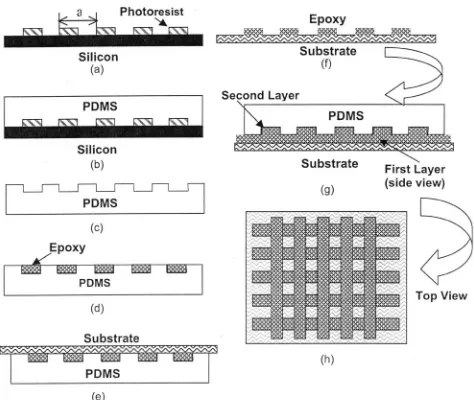
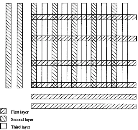
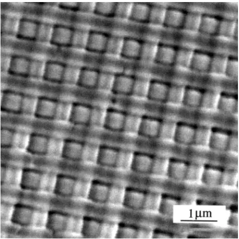
Fabrication of photonic band gap crystal using microtransfer molded templates
Full text
Figure
Related documents
Lymphatic malformations of the head and neck in adults: a case report and review of the literature. Surgical management of adult-onset cystic hygroma in the
The calibrated model predicted, with current screening practices and in the absence of vaccination, an annual number of 104,852 cases of HPV6/11 related genital warts in both males
To assess the intelligence level of orphan and non-orphan children and study the effects of genetic and environmental influences on Intelligence
While low doses of epinephrine and ADP used solely caused only low platelet response (their action did not differ from control), they exhibited summation of
In conclusion, this study demonstrates an association between GGT and elevated hsCRP levels among asymptomatic individuals, independent of obesity, metabolic syndrome and
Other activities/organizations: past co-president for PCA’s PPO; 2 nd -4 th grade teacher at PCA Summer Camp; Professional Development seminars in Everyday Mathematics and
Similarly, even if lawyers or trained and supervised laypersons were available to manually search ESI, they would likely be challenged by the volume of e-documents
