International Journal of Innovative Technology and Exploring Engineering (IJITEE) ISSN: 2278-3075, Volume-8 Issue-11, September 2019
Implementation of Low Power High Speed Adder’s
using GDI Logic
Addanki Purna Ramesh
Abstract- Addition is a vital arithmetic operation and is the base of other arithmetic operations such as multiplication, subtraction and division. Adder is a digital circuit that does addition of binary numbers. The 1-bit full adder is the basic block of an arithmetic unit. In VLSI, there are many efficient techniques to design digital circuits. Some of the techniques are Pass Transistor logic (PTL), Complementary metal oxide semiconductor (CMOS) and Transmitter gate (TG). There are several adder designs implemented to reduce the power. However, each design undergoes from precise disadvantage. The adder design with good driving capability requires more power and the design with more delay which consumes less power. In this paper 8-bit Carry Increment Adder (CIA), Carry Bypass Adder (CBA), Carry Skip Adder (CSKA), Carry Look Ahead Adder (CLA), Kogge Stone Adder (KSA), Han Carlson Adder (HCA), and Brent Kung Adder (BKA) are implemented using Gate Diffusion Input (GDI) logic. These designs are simulated and implemented using Tanner tool. The result shows that CBA, CLA, and KSA designs using GDI logic are more efficient compared to CMOS logic in view of power consumption, delay, and area (transistors count) respectively.
Keywords- Adder, Addition, GDI, CMOS, Power
consumption
I. INTRODUCTION
In VLSI, adders are the elementary building blocks of the arithmetic operations. Adders are commonly used in ALU, CPU, and floating point units. The half and full adders are the basic adders. Generally these circuits are implemented using CMOS logic, it has an important characteristic i.e., high noise immunity. The speed and complexity of the circuits increases the power consumption. The demand for movable apparatus like laptops and mobile phones is increasing rapidly, so low power and area efficient circuit designs are required with high speed, high reliability, small in size, longer battery life. Power and area is the regulating factor in both high performance and portable systems.
II. LITERATURESURVEY
Gate Diffusion Input (GDI) logic replaced the CMOS Logic for low power applications. This GDI logic reducing delay, area, and power consumption of digital circuits with low complexity of logic. CMOS circuits are built in such a way that PMOS transistors must have either a PMOS transistor or input from the voltage source. Similarly, NMOS transistors must have either an NMOS transistor or input from ground. Whereas GDI logic contains 3 inputs’ G, P and N Several logic utilities implemented using GDI logic (only two transistors) is shown in table 1.
Revised Manuscript Received on September 03, 2019
Addanki Purna Ramesh, Professor, Department of ECE, Vishnu
[image:1.595.352.496.142.264.2]Institute of Technology, Bhimavaram, India [email protected]
Figure 1: Schematic Diagram of GDI Logic
Table 1: Several logic utilities of GDI Logic Configurations for Input
In this work implementing 8-bit CIA, CBA, CSKA, CSA, CLA, KSA, HCA, and BKA are implemented using GDI logic using Tanner tool.
III. PROPOSEDWORK
A. Carry Increment Adder
The block diagram of CIA is shown in figure 2. The 8-bit CIA contains two 4-bit Ripple Carry Adders (RCA). The 1st RCA adds a required number of 1st 4-bit inputs producing sum and carry. Now the carry out of the 1st RCA is applied to Cin of the conditional increment block. Thus the
1st 4-bit sum is straightly taken from the ripple carry output. The 2nd RCA makes the addition operation irrespective of the 1st RCA output and will give out results which are fed to the conditional increment block. The input Cin to the 1st
RCA is at all times low value. The conditional increment block comprises of half adders. Based on the value of Cout of
[image:1.595.338.510.301.487.2]Implementation of Low Power High Speed Adder’s using GDI Logic
Figure 2: Block Diagram of CIA B. Carry Bypass Adder
The block diagram of CBA is shown in figure 3. In RCA, each full adder waits for the incoming carry to generate an outgoing carry. This need can be removed by presenting an extra bypass to speed up the action of the adder. An incoming carry Ci,0=1 transmits through whole
adder chain and causes an outgoing carry C0,7=1 below the
conditions that all transmission signals are 1. The operation of the adder can be speed up using this data. When P0P1P2P3P4P5P6P7 = 1, the incoming carry is sent to the next
block through the bypass and if it is not the case, the carry is obtained via the normal route. If (P0P1 P2P3P4P5P6P7 = 1)
then C0,7 = Ci,0 else either generate or delete happened. In
[image:2.595.318.533.70.246.2]CBA, full adders are separated into groups, each of them is “bypassed” by a mux, when all the full adders are in propagating.
Figure 3: Block Diagram of CBA C. Carry Skip Adder
The block diagram of CSA is shown in figure 4. A CSKA consists of a RCA with a skip chain used to speed up the carry chain. This chain explains the sharing of ripple carry blocks, which comprise the skip adder. The worst case for a RCA occurs, when the transmit stateis true for each pair (ai, bi). For each operand input bit pair (ai, bi) the
transmit conditions are determined using an XOR gate. When all transmit conditions are true, then the carry-in bit determines the carry-out bit. The n-bit CSKA consists of mux, AND gate with n-inputs and n-bit carry ripple chain. The carry ripple chain provides transmit bit, which is
[image:2.595.319.531.452.638.2]as a select bit that changes either the in to the carry-out signal or last carry bit.
Figure 4: Block Diagram of CSKA D. Carry Look Ahead Adder
The figure 5 shows the block diagram of CLA. The CLA computes carry bits before the sum, which decreases the wait time to compute the result of the higher bit value. In CLA to make addition much faster, propagate and generate logics are able to generate carries before the sum is produced. Full adder circuit develops two logics carry Generate (Gi = Ai AND Bi), and carry propagate (Pi = Ai XOR Bi). The output can be conveyed as sum (Si = Pi XOR Ci) and carry (Ci+1 = Gi + PiCi). Gi=carry generate and Pi=carry propagate, because it is term associated with the propagation of the carry from Ci to Ci+1. The carry output of each stage is C2 = G1+P1C1, C3 = G2+P2C2 = G2+P2 (G1+P1C1) = G2+P2G1+P2 P1C1, C4 = G3+P3C3. C4, C3 and C2 are transmitted at the same time. Each output carry are expressed in sum of product form.
Figure 5: Block Diagram of CLA E. Kogge Stone Adder
[image:2.595.60.281.481.595.2]International Journal of Innovative Technology and Exploring Engineering (IJITEE) ISSN: 2278-3075, Volume-8 Issue-11, September 2019
Figure 6: Block Diagram of Parallel Prefix Adders
The pre-processing stage is used to estimate generate and propagate bit, The carry computation stage is used to compute the carry bit and the post processing stage to calculate the sum bit. The most used parallel prefix adders are KSA, HCA and BKA. KSA is a parallel prefix form of CLA. It produces carry in zero time. The preprocessing stage in KSA Generate (pi, gi) from (Ai, Bi). pi = Ai XOR Bi, gi = Ai AND Bi. The logic equations in carry computation stage are Pi:j = Pi:k+1 and Pk:j, Gi:j = Gi:k+1 or (Pi:k+1 and Gk:j ), Ci = Gi:0 or (Cin and Pi:0). The logic equations in post processing stage is Si = Pi xor Ci‐1.
The HCA and BKA are ALSO parallel prefix adders having the same procedure of KSA but with different architecture.
IV.RESULTS
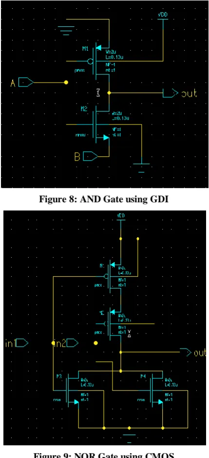
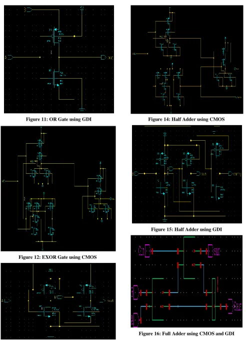
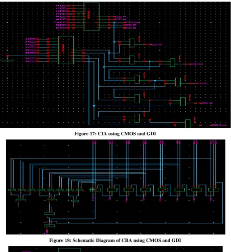
The schematic diagrams of AND, NOR, OR, and EXOR gates, basic modules of half adder and full adder, 8-bit CIA, CBA, CSKA, CLA,KSA, HCA, and BKA are shown in figures 7 to 23 respectively using Tanner. In the architecture of CMOS adders, the CMOS basic modules like AND, NOR, OR, and EXOR gates, half and full adders are used. The architecture of GDI adders is same as CMOS adders but CMOS basic modules are replaced with GDI basic modules.
Figure 7: AND Gate using CMOS
Figure 8: AND Gate using GDI
[image:3.595.68.271.55.238.2]Figure 9: NOR Gate using CMOS
[image:3.595.68.269.561.736.2]Implementation of Low Power High Speed Adder’s using GDI Logic
Figure 11: OR Gate using GDI
Figure 12: EXOR Gate using CMOS
Figure 13: EXOR Gate using GDI
Figure 14: Half Adder using CMOS
[image:4.595.53.546.40.721.2]Figure 15: Half Adder using GDI
International Journal of Innovative Technology and Exploring Engineering (IJITEE) ISSN: 2278-3075, Volume-8 Issue-11, September 2019
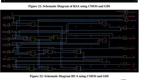
[image:5.595.68.529.47.551.2]Figure 17: CIA using CMOS and GDI
Figure 18: Schematic Diagram of CBA using CMOS and GDI
Implementation of Low Power High Speed Adder’s using GDI Logic
[image:6.595.78.522.268.502.2]Figure 20: Schematic Diagram of CLA using CMOS and GDI
Figure 21: Schematic Diagram of KSA using CMOS and GDI
[image:6.595.75.542.490.747.2]International Journal of Innovative Technology and Exploring Engineering (IJITEE) ISSN: 2278-3075, Volume-8 Issue-11, September 2019
Figure23: Schematic Diagram of BKA using CMOS and GDI
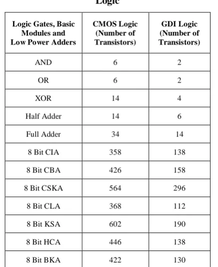
[image:7.595.61.279.498.765.2]The transistors count, delay, and power consumption of logic gates, basic modules and low power adders using CMOS and GDI logic are shown in tables 2 to 4 respectively.
Table 2: Transistors Count for Logic Gates, Basic Modules & Low Power Adders using CMOS and GDI
Logic
Logic Gates, Basic Modules and Low Power Adders
CMOS Logic (Number of Transistors)
GDI Logic (Number of Transistors)
AND 6 2
OR 6 2
XOR 14 4
Half Adder 14 6
Full Adder 34 14
8 Bit CIA 358 138
8 Bit CBA 426 158
8 Bit CSKA 564 296
8 Bit CLA 368 112
8 Bit KSA 602 190
8 Bit HCA 446 138
8 Bit BKA 422 130
Table 3: Delay for Logic Gates, Basic Modules & Low Power Adders using CMOS and GDI Logic
Logic Gates, Basic Modules and Low Power Adders
CMOS Logic (Sec)
GDI Logic (Sec)
AND 2.47 2.06
OR 2.69 2.34
XOR 2.92 2.34
Half Adder 3.23 2.46
8 Bit CIA 5.48 2.49
8 Bit CBA 6.38 2.58
8 Bit CSKA 5.33 2.78
8 Bit CLA 7.86 3.94
8 Bit KSA 6.95 3.29
8 Bit HCA 9.53 4.08
Implementation of Low Power High Speed Adder’s using GDI Logic
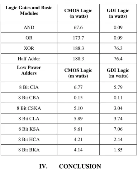
Table 4: Power Consumption of Logic Gates, Basic Modules & Low Power Adders using CMOS and GDI
Logic
Logic Gates and Basic Modules CMOS Logic (n watts) GDI Logic (n watts)
AND 67.6 0.09
OR 173.7 0.09
XOR 188.3 76.3
Half Adder 188.3 76.4
Low Power
Adders CMOS Logic
(m watts)
GDI Logic (m watts)
8 Bit CIA 6.77 5.79
8 Bit CBA 0.15 0.11
8 Bit CSKA 5.10 3.04
8 Bit CLA 5.89 3.74
8 Bit KSA 9.61 7.06
8 Bit HCA 4.21 2.44
8 Bit BKA 4.14 1.85
IV. CONCLUSION
In this work 8-bit CIA, CBA, CSKA, CLA, KSA, HCA, and BKA are implemented in CMOS and GDI logic using Tanner. Analyzing the results CLA, KSA, and CBA designs using GDI logic are more efficient compared to CMOS logic in terms of area (transistors count), delay, and power consumption respectively. Whereas CIA, CBA, CSKA, CLA, KSA, HCA, and BKA adders using GDI logic requires 61.45%, 62.91%, 62.96%, 69.56%, 68.43%, 69.05%, and 69.19% less number of transistors compared to CMOS logic respectively. The delay of CIA, CBA, CSKA CLA, KSA, HCA, and BKA adders using GDI logic 54.56%, 52.44%, 47.84%, 56.34%, 57.19%, 52.53%, 49.88% less compared to CMOS respectively. The CIA, CBA, CSKA, CLA, KSA, HCA, and BKA adders using GDI logic consumes 14.47%, 26.67%, 40.39%, 36.51%, 26.54%, 42.05%, and 55.32% less power compared to CMOS logic respectively. In respect of number of transistors, delay, and power consumption out of seven adders CLA, KSA, and BKA adders requires 69.56%, 57.19%, and 55.32% less compared to other adders. So CLA, KSA, and BKA adders are best in area, delay, and power efficient adders compared to other adders.
REFERENCES
1. S Bharathi “Area Efficient Self Timed Adders for Low Power Applications in VLSI”, I. J. of innovative Research in Science, Engg and Technology, Vol. 4, Issue 2, Feb 2015.
2. Jashanpreet kaur, et.al. “A Review on GDI”, I. J of Advance Research in Electronics, Electrical & Computer Science Applications of Engg & Technology, Vol. 2, Issue 4, July 2014.
3. P.Chaitanya Kumari, “Design of 32 bit Parallel Prefix Adders”, IOSR Journal of Electronics and Communication Engg, Vol.6, Issue 1, May 2013.
5. Arun Prakash Singh, “Implementation of 1-Bit Full Adder using GDI Cell”, I.J.of Electronics and Computer Science Engineering, Vol.1, Issue 2,pp.333-342, 2012.
6. Madhu Thakur, “ Design of Braun Multiplier with KS A & its Implementation on FPGA”, I.J. of Scientific & Engg Research, Vol.3, Issue 10, Oct-2012.
7. S. Veeramachaneni, “Efficient Design of 32-Bit Comparator using CLA Logic,” in Proceedings of the IEEE NEWCAS ’07, August 2007, pp.867–870.
AUTHORSPROFILE
Addanki Purna Ramesh has more than