City, University of London Institutional Repository
Citation
:
Viphavakit, C., Boonruang, S., Themistos, C., Komodromos, M., Mohammed, W.
S and Rahman, B. M. (2016). Surface plasmon resonance-enhanced light interaction in an
integrated ormocomp nanowire. Optical and Quantum Electronics, 48(5), doi:
10.1007/s11082-016-0499-9
This is the accepted version of the paper.
This version of the publication may differ from the final published
version.
Permanent repository link:
http://openaccess.city.ac.uk/14661/
Link to published version
:
http://dx.doi.org/10.1007/s11082-016-0499-9
Copyright and reuse:
City Research Online aims to make research
outputs of City, University of London available to a wider audience.
Copyright and Moral Rights remain with the author(s) and/or copyright
holders. URLs from City Research Online may be freely distributed and
linked to.
Surface plasmon resonance
-
enhanced light
interaction in an integrated ormocomp nanowire
Charusluk Viphavakit,1* Sakoolkan Boonruang,2 Christos Themistos,3 Michael Komodromos,3 Waleed
S. Mohammed,4 and B.M.Azizur Rahman1
1 School of Mathematics, Computer Science and Engineering, City University London,
Northampton Square, London EC1V 0HB, UK
2Photonics Technology Laboratory, Thailand National Electronics and Computer Technology Center (NECTEC), Klong
Luang, 10120, Pathumthani, Thailand
3 Department of Electrical Engineering, Frederick University, 7 Frederickou Str., Nicosia, 1036, Cyprus 4Center of Research in Optoelectronics, Communication and Control System (BU-CROCCS), Bangkok University,
Paholyotin Rd., Klong Luang, 10120, Pathumthani, Thailand *Corresponding author: [email protected]
An integrated ormocomp nanowire coated with gold metal layer is proposed and its optical characteristics with the effect of surface plasmon resonance (SPR) are studied. The integrated rib-like nanowire has a trapezoidal shape with sidewall angles of 75. It is coated with 50 nm gold layer to introduce the SPR and enhance the evanescent field in the sensing region located at the dielectric/metal interface. The possible field modes, the normalized power confinement, and the SPR peak position of the nanowire are studied over the wavelength and the metal thickness by using the full-vectorial H-field FEM in quasi-TM mode. The attenuation coefficient of the nanowire, the SPR
peak wavelength, and the wavelength shift is experimentally extracted for three different cladding materials. The redshift of the supermode coupling between the dielectric mode and the anti-symmetric supermode is observed with the higher cladding-index and larger metal thickness. The improvement of the power confinement in the
sensing region with the SPR effect is ten times (10x) better than a previous similar study.
Keywords: Polymer waveguides; Subwavelength structures; Integrated optics devices; Optical design and fabrication.
1. Introduction
Nanowires are one-dimensional structures exhibiting a high
aspect ratio (≥1000). They are considered as a good candidate for nanotechnology applications due to their unique properties of high surface-to-volume ratio (Shen et al. 2009; Yun et al. 2003;
Themistos et al. 2009). In photonics, nanowires are used as optical waveguides, and particularly silicon-on-insulator (SOI)
based nanowires have been used as optical sensors because they have the advantage of high index contrast and low optical power losses (Dell’Olio,Passaro 2007; Sirbuly et al. 2006; MacCraith et al. 1991; Lou et al. 2005; Wang,Dai 2010).
Recently, polymer nanowires are alternatively being used as optical waveguides in sensing applications due to their attractive features. Polymer nanowires have better mechanical flexibility compared to semiconductor nanowires and they are biocompatible materials which can have different functional dopants (Adhikari,Majumdar 2004; Viphavakit et al. 2014b). Their fabrication process can be simpler than those of glass nanowires. Hence, they can be used in a variety of possible sensing applications. By exploiting their chemical selectivity, polymer nanowires can be used to detect a wide range of chemical compounds including toxics gases, metal ions, and DNA (Huang et al. 2003; Wang et al. 2002; Ramanathan et al. 2005). Polymer nanowires have been studied for use as chemical sensors, biosensors, organic light emitting diodes, and organic solar cells (Huang et al. 2003; Liu et al. 2004; Ramanathan et al. 2005). It has been reported that polymer nanowires can be used
in humidity sensing and NO2 and NH3 detection with 30ms
response time and high sensitivity (Gu et al. 2008). The use of fluorescent polymer nanofibrous to detect the metal ions (FE3+
and Hg2+) has been reported (Wang et al. 2002). The polymer
nanowires can also be modified as electrical conductors and used to detect NH3 gas at concentrations as low as 0.5 ppm (Liu et al.
2004).
The attenuation loss of nanowires can be due to volume absorption and surface scattering (Tien 1971). The polymer nanowires examined in earlier work (Viphavakit et al. 2014a), with dimensions similar to those of the structures presented in this paper, exhibited surface scattering, caused by the surface roughness which has been considered as the dominant factor to enhance the evanescent fields and the sensitivity. However, the sensitivity of polymer nanowires can be further improved by coating a thin metal layer on the top surface which introduces surface plasmon resonance (SPR) (Fukuda et al. 2010). It has been reported that the optical transmission through the sub
-wavelength holes in the metal film can be increased by an additional factor of 10 (Krishnan et al. 2001). The use of colloidal Au as a nanoparticles tag for the detection of DNA hybridization has shown great improvement in the sensitivity compared to those without Au (He et al. 2000). The use of localized surface plasmon resonance (LSPR) to enhance the sensitivity of the waveguides for biosensors has also been addressed (Byun et al. 2005; Kim et al. 2006). A low propagation loss can be achieved by exhibiting the long-range surface plasmon polarition (LR-SPP) in
-Zehnder interferometer for glycerin-water solutions is
significantly improved to 5.5x10⁻⁸ RIU per 0.01 phase change (Wu et al. 2004). Also with SPR, it has been reported that 2 ng of nCG presence in 1 ml of 1% bovine serum albumin solution can be detected with a small refractive index change which is less than 1.2x10⁻⁶ (Dostalek et al. 2001).
The design of gold coated polymer nanowires, the characterization of their guided modes using finite element method (FEM) and the experimental measurements of their optical characteristics obtained are presented in the this work. The polymer nanowires examined are considered to be trapezoidal, as shown in Fig. 1(a), with their height to be about 0.5 µm and the top and bottom widths, 1.0 and 1.5 µm, respectively, with the dimensions of their guided area, being much smaller than the core diameter of single mode fibers (SMF). Therefore, the polymer nanowires with the integrated optics structure are designed in order to minimize the power losses occurred when launching the light from the source into the nanowires. Also, the integrated optics structure allows the nanowires to be easily used with other optical devices for sensing applications. In this paper, the polymer nanowires coated with a thin metal layer are intended to be used as optical transducers to detect the change of effective index when the cladding-index is
varied.
The nanowires were fabricated using ormcomp, which is a hybrid-polymeric material. It is a UV-curable material with
refractive index of 1.52. The fabrication of the polymer nanowires used in this study is implemented by the nano-imprint method
which has been described earlier (Viphavakit et al. 2014a). The gold metal layer is deposited on the surface of the nanowires using sputtering where its refractive index is wavelength dependent.
In the present work, a full-vectorial H-field FEM is used to
study the propagation characteristics of the guided modes, their normalized power confinement in the sensing region, and their resonance peak over the operating wavelength with the thickness of metal layer, and the cladding-index. The sensing
area is considered to be the cladding/gold interface.
The experimental part consists of the attenuation coefficient extraction, the determination of the SPR peak wavelength and its shift. The cladding materials used are water and iso-propanol
solution with different volume ratios. A comparison of the SPR peaks at some specific cladding-indices between the simulation
results and the experimental results based on the metal thickness are also presented. With the SPR, the normalized power confinement in the sensing region is significantly increased at the resonance wavelength. Hence, the sensitivity of the ormocomp nanowires coated with gold is improved compared to those without gold layer.
2. Design of the Nanowires
The ormocomp polymer nanowires were fabricated using the nano-imprint method (Viphavakit et al. 2014a). A silicon
nanowire is used as a master mold in the nano-imprint process.
The master mold silicon nanowire results in slanted sidewalls from the anisotropic wet etching along the crystal plane. Consequently, the non-vertical sidewalls ormocomp nanowires
are considered and their optical imaging and optical properties including the attenuation coefficient are studied. The surface roughness, as a result of the fabrication process, enhances the sensitivity of the non-vertical sidewalls ormocomp nanowires
(Viphavakit et al. 2014a). The effect of the surface roughness is not strong enough to maximize the sensitivity of the nanowires. However, the sensitivity can be improved by introducing surface plasmon resonance at the top surface of the nanowires where the evanescent field exists.
In this paper, we present the effect of surface plasmon resonance (SPR) to the non-vertical sidewalls ormocomp
nanowires. A thin gold layer with the thickness of 50 nm is coated on the nanowires using the sputtering technique. Due to the slanted structure, the gold layer covers both the top surface and the sidewalls. A cross-section of the non-vertical sidewalls
nanowire coated with gold layer is presented in Fig. 1(a). The ormocomp nanowire structure has height 0.5 µm. The top and bottom widths of the trapezoidal core are 1.0 µm and 1.5 µm, respectively. The ormocomp nanowires have rib-shaped structure
due to the leftover ormocomp layer from the stamping process in the nano-imprint (Viphavakit et al. 2014a). The sidewall angle ()
is measured to be around 75. The gold layer at the top surface has a uniform thickness of 50 nm. The nanowires are designed to be easily used with other optical devices, such as optical couplers, by having feed waveguides and tapered waveguides attached to their ends as shown in Fig. 1(b).
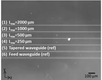
The integrated nanowire structure shown in Fig. 1 has length
Fig. 1: (a) A cross-section of the nanowire structure coated with thin metal layer. The rib-shaped nanowire has non-vertical sidewalls. The structure height is 0.5 m. The metal layer has the thickness of 50 nm. (b) A top
-view of an integrated nanowire connected to a feed waveguide and a tapered waveguide.
[image:3.612.322.560.59.222.2] [image:3.612.350.526.557.695.2]Lo = 5000 µm. It consists of a feed waveguide (Lwg), a tapered
waveguide (Ltp) with a length of 270 µm and the nanowire (Lnw)
with a length in a range of 250 µm to 2000 µm. To study the optical properties of the nanowire such as the attenuation coefficient (nw), a set of nanowires containing nanowires with
different lengths is designed and fabricated, as presented in Fig 2. The nanowire set has one reference feed waveguide, one reference tapered waveguide, and four nanowires with lengths of 250, 500, 1000, 2000 µm.
Even though the sidewalls of the trapezoidal shape nanowires are coated with a layer of gold, the sidewall angle is large enough to neglect the thickness of the gold layer at the sidewalls. Hence, the surface plasmon resonance effect is dominant at the top surface (TM mode) while the effect of the surface plasmon resonance at the sides is negligible (TE mode). It was also observed experimentally that there was no significant TE mode SPR signal.
3. Simulation Results
Light propagation along the metal-coated nanowire can be
implemented via dielectric and plasmonic modes mainly propagating in the core region and the metal/dielectric interface, respectively. Plasmonic mode is generated when the momentum of photons matches with the momentum of the plasmons. The first order approximation resonance condition at the semi-infinite
dielectric/metal interface is given by (Raether 1988);
𝛽𝑠𝑝=2𝜋𝜆 √𝜀𝑚
′(𝜆)𝜀𝑐
𝜀𝑚′ (𝜆)+𝜀𝑐
(1)
where 𝛽𝑠𝑝 is the propagation constant for SPR mode. The
resonance occurs when the propagation constant of the guided mode equals to 𝛽𝑠𝑝, where 𝜆 is the operating wavelength in free
space. Note that 𝜀𝑚′ is the real part of the dielectric constant of the
metal, which is a wavelength dependent parameter, and 𝜀𝑐 is the
dielectric constant of the cladding material (𝜀𝑐 = 𝑛𝑐2). The surface
plasmon resonance exists when 𝜀𝑚′ is negative and its magnitude
is larger than 𝜀𝑐 (𝜀𝑚′ < 0 and |𝜀𝑚′| > 𝜀𝑐). As mentioned above the
ormocomp nanowires are coated with a gold layer of thickness of about 50 nm. For the SPR at the finite dielectric/metal interface, the analytical form of the resonance condition can be calculated from the incident light reflectivity where the metal thickness is the key parameter (Raether 1988). However, for the SPR on the metal-coated nanowire, the finite element method (FEM) is used
instead of the analytical approach for a 2-dimensional waveguide
and the metal thickness is also taken into consideration when 𝛽𝑠𝑝
is calculated.
The full-vectorial H-field finite element formulation has been
used to study and analyze the behavior of the ormocomp nanowires with the effect of the SPR in order to determine the propagation characteristics of the fundamental optical mode. The functional used to solve the problems is related to the standard eigenvalue problems, and the modal characterization is obtained by minimizing the functional as shown in Eq. 2 (Rahman,Davies 1984).
𝜔2=∫[(𝛻×H)∗∙𝜀−1(𝛻×H)+𝑝(𝛻∙H)∗∙(𝛻∙H)]𝑑𝑥𝑑𝑦
∫H∗∙𝜇H 𝑑𝑥𝑑𝑦 (2)
where H is the full vectorial magnetic field, * represents the complex conjugate and transpose, 𝜔 is the angular frequency of the wave, 𝜔2 is the eigenvalue, and 𝜀 and 𝜇 are the permittivity
and permeability, respectively. In this work, 125,000 first order triangles are used to represent the one half of the nanowire structure by exploiting the existing one-fold symmetry. The main advantage of the FEM over the other numerical methods is that it can incorporate triangles of different shapes and sizes to achieve numerical efficiency. In our case, vertical resolution of 0.8 nm or better is achieved for the 50 nm thick metal layer.
In the numerical simulations the ormocomp nanowires are assumed to be coated with a 50 nm gold layer only at the top surface. Therefore, only the quasi-TM mode (Hx ) is considered.
For the quasi-TM mode, the dominant electric field component,
Ey, is perpendicular to the dielectric/metal interface. The possible
mode fields and power confinement of the ormocomp nanowires with the effect of SPR are studied over the wavelength for different cladding materials. Ormocomp is a transparent hybrid
-polymer material with the refractive index n=1.52. The complex refractive index of gold (𝑛̃ = 𝑛 + 𝑖𝜅) is dependent on the operating wavelength (Wooten 2013). We consider the visible region (400
-700 nm) in this work. According to the experimental work, water (n=1.333) and two different volume ratios of iso-propanol solution
(n=1.351 and n=1.365) are considered as the cladding materials. As it was mentioned above, the ormocomp nanowires were fabricated using nano-imprint method and they have trapezoidal
shape cross-section, with the fixed dimensions of 0.5 µm height,
1.5 µm bottom-width, and 1.0 µm top-width (Viphavakit et al.
2014a).
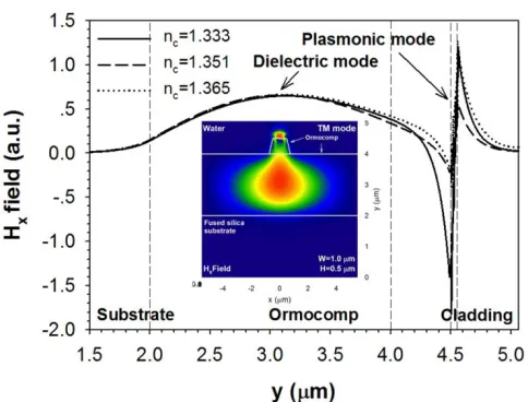
The two possible optical modes in the nanowire structures are the dielectric mode inside ormocomp region and the plasmonic mode at the dielectric/metal interface. These two modes can be clearly separated or coupled with each other to create a supermode depending on the parameters of the nanowire structure, especially the height of the nanowire. In the case of nanowires with height 0.5 µm, the coupled dielectric-plasmonic
mode is shown in Fig. 3, where the supermode coupling between the dielectric mode and the odd-like plasmonic supermode can be
clearly seen from the Hx profile along the y-direction. The inset
shows the Hx-field contour plot of the coupled mode with water
cladding.
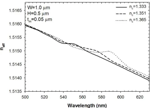
Variations of the effective indices of the fundamental Hx modes
[image:4.612.318.560.50.234.2]in three different cladding mediums with respect to the operating
Fig. 3: The Hx of the coupled dielectric-plasmonic mode along the y-axis for
wavelength are shown in Fig. 4. The effective indices of the optical mode decrease when the wavelength is increased regardless of the cladding-index because the wavelength becomes
larger compared to the dimension of the nanowire. However, from the characteristics of the effective indices, particularly the peak at some specific wavelengths, it can be used to identify the SPR wavelengths. Effective index of the plasmonic mode is normally higher than that of the fundamental dielectric mode. Hence, the effective index of the coupled dielectric-plasmonic
mode occurring at a certain wavelength is slightly higher than that of the dielectric mode alone.
At the wavelength where the SPR occurs, the power confinement in the sensing region which is at the gold/cladding interface also increases because the evanescent field at the interface is enhanced. The variation of the normalized power confinement in the sensing area with the wavelength is shown in Fig. 5. The power confinement in the sensing region of the gold
-coated ormocomp nanowire in water-cladding for quasi-TM mode
is 10 times higher than the ormocomp nanowire with the same parameters but without gold layer which was examined in our previous study (Viphavakit et al. 2014a).
The resonance peak wavelength at which the SPR signal occurs for each cladding material can be recognized from the peak in both the effective index and power confinement graphs. In case of water-cladding, the SPR signal is obtained at 𝜆 =551
nm. However, the plasmonic modes in iso-propanol solution are
observed at 𝜆 =576 nm and 𝜆 =590 nm for the cladding-indices of
1.351 and 1.365, respectively. As the cladding-index increases, a
redshift of the SPR peak wavelength is observed. Besides the cladding material, the thickness of the metal layer is another important parameter which also affects the resonance peak position.
For gold-coated nanowires, the SPR occurs at both the
nanowire/metal and cladding/metal interfaces. These two plasmonic modes can be coupled to the supermode of symmetric or antisymmetric resonance. With thicker metal layer, the antisymmetric surface plasmon has a redshift while the symmetric surface plasmon obtains a blueshift (Tang,He 2011). In this paper, the antisymmetric mode (odd mode) as shown in Fig. 3 is considered. The relation between the SPR peak wavelengths for each cladding material with different metal thickness for an odd-plasmonic supermode is shown in Fig. 6.
The metal thicknesses of 50, 60, and 70 nm are considered to check for the resonance peaks and their shifts. At a very thin metal layer, the enhancement of the evanescent fields by SPR is less compared to that with thicker metal layer. However, if the thickness of the metal layer is too large, the coupling between the two surface plasmon modes is weaker. Hence, the power confinement and sensitivity at the cladding/metal interface is decreased. As it is seen in Fig. 6, the redshift of about 25-30 nm is
observed in each cladding-index when the metal thickness is
increased by 10 nm.
4. Experimental Results
The experimental results presented below include the extraction of the attenuation coefficient of the ormocomp nanowires (𝛼𝑛𝑤)
and the analysis of the SPR peak and its shift with the use of different cladding materials. The actual nanowires used in the experiment were fabricated using the nano-imprint method
(Viphavakit et al. ). The gold layer is coated on the ormocomp nanowires using the sputtering technique. The cladding
[image:5.612.315.552.52.230.2]Fig. 5: Variation of normalized power confinement in the sensing region of a nanowire for different cladding-indices with the operating wavelength. The highest power confinement is obtained at the SPR wavelength. Fig. 4: Variation of effective index of the gold-coated ormocomp nanowire
for different cladding materials with respect to the operating wavelength. The peaks indicate the wavelengths where the SPRs are introduced.
[image:5.612.55.297.56.230.2] [image:5.612.57.298.522.698.2]materials are water (n=1.333) and two iso-propanol solutions.
The iso-propanol solution is a mixture of water and iso-propanol.
For this paper, iso-propanol solutions with two different volume
ratios, 1:1 and 1:3, are used, yielding refractive indices of 1.365 and 1.351, respectively. The light source used in this experiment is a broadband light source where the operating wavelength is in visible wavelength (𝜆 =400-700 nm).
4.1 Extraction of Attenuation Coefficient
The ormocomp nanowire fabricated by using nano-imprint
method has non-vertical sidewalls with the sidewall angle of 75.
Therefore, the gold layer deposited using the sputtering technique at the sidewalls is thinner compared to the top surface due to the sidewall angle. This assumption is confirmed from the experimental work as there is no effect of SPR at the sidewalls (TE mode). The thin metal layer at the top surface introduces the coupling of SPR between the ormocomp/gold and cladding/gold interfaces in TM mode.
The optical setup shown in Fig. 7 is used to obtain the attenuation coefficient of a gold-coated ormocomp nanowire.. The
spectrometer is used to measure the intensity of the transmittance signals. The white LED connected with a single mode optical fiber is used as a broadband light source (𝜆=400-700
nm). The input light from the light source is considered to be unpolarized light, so a polarizer is needed in the optical setup in order to be able to select the TM mode signal for the SPR at the top surface of the nanowire. An objective lens with magnification of 20x is used to focus the light, and also enhance the input signal. In an alignment process, the objective lens with magnification of 10x is connected with the CCD camera, working as an optical microscope, is used to align the optical fiber and the nanowire on the glass substrate. After a successful alignment, the focused light is coupled into the specific nanowire, and then propagates along the wire. At the end of the nanowire, the output
signal is divided into two equivalent beams by the beam splitter. One signal is imaged by the CCD camera. Another output signal is detected by the spectrometer to measure the intensity of the light affected by SPR. The transmittance (𝑇) then can be obtained using the Beer-Lambert law given by
𝑇 =𝐼𝐼
𝑜= 𝑒
−𝛼(𝜆)𝐿
(3)
where 𝐼𝑜 is the intensity of the incident light, 𝐼 is the intensity of
the transmitted light. 𝛼 is the attenuation coefficient as a function of wavelength (𝜆) and 𝐿 is the path length. Air is considered to be the cladding material for the incident light because the SPR absorption wavelength in the air/metal
interface is in the IR region the above nanowires are operated in the invisible region.
As mentioned earlier, the nanowire is designed to be integrated with other optical devices, the feed and tapered waveguides at its ends. Therefore, the attenuation coefficient of the integrated nanowire (𝛼), consists of the attenuation coefficients from the feed waveguide (𝛼𝑤𝑔), the tapered
waveguide (𝛼𝑡𝑝) and the nanowire itself (𝛼𝑛𝑤). Therefore, the set
of integrated nanowires shown in Fig. 2 is needed. The set includes the reference feed waveguide, the reference tapered waveguide, and nanowires with different lengths, so the attenuation coefficient of the nanowire can be extracted individually. The attenuation coefficient of a nanowire (𝛼𝑛𝑤) can
be derived from Eq. 3 as stated below
𝛼𝑛𝑤(𝜆) =
−𝛼𝑤𝑔(𝜆)(𝐿𝑜−2𝐿𝑡𝑝−𝐿𝑛𝑤)−2𝛼𝑡𝑝(𝜆)𝐿𝑡𝑝−𝑙𝑛 (𝑇𝑛𝑤)
𝐿𝑛𝑤
(4)
where 𝐿𝑜 is 5000 μm and 𝐿𝑡𝑝 is 270 μm. The incident light (𝐼𝑜) and
the transmitted light (𝐼) are the light propagating in the nanowires with aircladding and water cladding, respectively. The transmittance of the integrated nanowires (𝑇𝑛𝑤) with
different lengths, 𝐿𝑛𝑤= 250, 500, 1000, and 2000 µm, obtained
with the spectrometer is presented in Fig. 8.
It can be seen that the longest nanowire (𝐿𝑛𝑤=2000 µm)
represented in solid line has the smallest transmittance. The dotted line represents the shortest nanowire (𝐿𝑛𝑤=250 μm). It
has the highest transmittance. It can be concluded that the longest nanowire has the highest SPR absorption. Using the
[image:6.612.317.559.51.238.2]Fig. 7: (a) Schematic showing the optical setup to measure the transmittance signal. (b) The actual optical setup and the gold-coated ormocomp nanowires.
Fig. 8: The transmittance of the gold-coated nanowires with lengths 250,
[image:6.612.49.295.52.295.2]transmittance value from Fig. 8 together with Eq. 4, the attenuation coefficient of the feed waveguide and nanowire can be obtained seperately as presented in Fig. 9.
The average attenuation coefficient of the nanowires (dashed line) and the feed waveguides (solid line) is presented in Fig. 9. The absorption peak for both the feed waveguide and the nanowires are found to occur at 𝜆 =590 nm. The feed waveguide has absorption coefficient of 𝛼𝑤𝑔=1.03x10⁻⁴ µm-1, which is lower
than the absorption coefficient of the nanowires 𝛼𝑛𝑤=1.93x10⁻⁴
µm-1, since the feed waveguides are multimode and the nanowires are single mode waveguides. In the multimode waveguide the power is distributed in many modes, causing a reduction of optical power in each mode. In addition, each mode has different SPR momentum. Therefore, the absorption peak of the SPR in each mode is located at different wavelength, causing the broadening of the absorption peak in the feed waveguide.
4.2 Analysis of the SPR peak
As described earlier in the previous section, the optical modes
examined in the nanowires are the coupled supermode between the dielectric mode and the plasmonic mode. In addition, the plasmonic mode itself is also a supermode due to coupling between two surface plasmon modes at the ormocomp/gold and cladding/gold interfaces. It is sensitive to the change of the cladding index which can be studied by investigating the wavelength shift with different refractive indices of cladding materials. The cladding materials used in this study are water (n=1.333), and the iso-propanol solutions. The solutions are
prepared with different volume ratio of iso-propanol to water.
[image:7.612.318.555.53.235.2]With 1:1 volume ratio, the solution has refractive index of 1.365 and the index of 1.351 is measured for the ratio of 1:3. The transmittance is measured again for different cladding materials. Then, the attenuation coefficient of a nanowire showing the SPR peak wavelength for three cladding materials is illustrated in Fig. 10.
As the cladding-index increases, the SPR peak is shifted to a
higher wavelength. According to the simulation results, the redshift occurs with the higher refractive index of cladding material.
The attenuation coefficient of the gold-coated nanowires (𝛼𝑛𝑤)
is affected by three factors which are the scattering (𝛼𝑠𝑐𝑎𝑡𝑡𝑒𝑟𝑖𝑛𝑔) from the surface roughness, the SPR (𝛼𝑆𝑃𝑅) from the thin gold
layer and the coupling loss (𝛼𝑐𝑜𝑢𝑝𝑙𝑖𝑛𝑔) from light source coupling into the nanowire. The attenuation coefficient of the gold-coated
can be derived as presented below.
𝛼𝑛𝑤= 𝛼𝑠𝑐𝑎𝑡𝑡𝑒𝑟𝑖𝑛𝑔+ 𝛼𝑆𝑃𝑅+ 𝛼𝑚𝑎𝑡𝑒𝑟𝑖𝑎𝑙 𝑎𝑏𝑠𝑜𝑟𝑝𝑡𝑖𝑜𝑛
(5)
The attenuation coefficient of the gold-coated nanowires
increases when increasing the refractive index of the cladding materials, unlike the attenuation coefficient of the non-coated
ormocomp nanowires which is reduced when the cladding index increases (Viphavakit et al. 2014a). Therefore, the SPR is the dominant factor that affects the attenuation coefficient in the gold-coated ormocomp nanowires while the scattering from the
surface roughness is the main factor for the non-coated
nanowires (Viphavakit et al. 2014a). The power loss from material absorption can be negligible because ormocomp has very
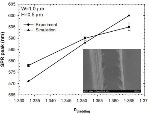
Fig. 11: The comparison of the SPR peak wavelength between the experimental result and the simulation result at three cladding materials. The peak position of the nanowire coated with metal thickness of 55 nm is the best match with the experimental work. An inset shows the surface roughness of the gold coated nanowire.
Fig. 9: Variation of the average attenuation coefficient of the feed waveguide and ormocomp nanowires with respect to wavelength for the water cladding. The nanowire has higher SPR absorption compared to the wider feed waveguide.
[image:7.612.52.294.53.230.2] [image:7.612.54.290.519.691.2]low absorption in the visible region (UV-Curable Hybrid Polymers for Micro Optical Components).
The average SPR peak wavelength for those three cladding materials is shown in Fig. 11. The comparison of the peak position between the simulation and experimental results is also presented in Fig. 11. From the experimental work, the SPR peak wavelength for the water cladding (n=1.333) was found to be about 𝜆 =578±0.5 nm. For iso-propanol solution cladding with
refractive index of 1.351 the peak position is at 𝜆 =590±0.9 nm. For the largest cladding-index in this work (n=1.365), the SPR is
observed at the wavelength of 𝜆 =595±1.7 nm. The SPR peak from the experiment is compared with the 55 nm gold-coated
nanowire in the simulation. The comparison shows the same trend of the peak redshift with the claddingindex. However, the effect from the large surface roughness due to the fabrication process has to be taken into account for the experimental works. The surface roughness of the nanowire is about 0.1-0.2 µm as
shown in the inset of Fig. 11.
5. Conclusion
The effect of SPR on the integrated ormocomp nanowire coated with a 50 nm thick layer of gold is studied both through simulations and experiments. The nanowire is designed to be attached with a feed waveguide and a tapered waveguide at its ends so it can be used as an integrated optics device. The fabricated nanowire has a trapezoidal shape with height 0.5 µm, bottom width 1.5 µm and top width 1.0 µm. The sidewall angle is about 75. The cladding materials in this work are water and two different volume ratios of iso-propanol solutions. The operating
wavelength is in the visible region (400-700 nm). The full
-vectorial H-field FEM is used in the simulations to study the
modal field and the normalized power confinement of the nanowires with vertical resolution of 0.8 nm in the sensing region. The optical modes presented are the coupled supermode between the dielectric mode in the ormocomp nanowire and the plasmonic supermode. For the thin metal layer coated nanowires, the two plasmonic modes at the ormocomp/gold and cladding/gold interfaces are coupled and form a symmetric or an antisymmetric mode (odd or even mode). In this paper, the odd
-like plasmonic supermode is considered. Even though the ormocomp nanowire has a rib-like structure and the optical field is extended inside the slab layer, the plasmonic mode is more significant compared to the dielectric mode at the SPR peak wavelength. The SPR peak wavelength is clearly observed and the redshift occurs when the refractive index of the cladding material is increased for both simulation and experimental results. The peak position also depends on the thickness of the metal layer. With a thicker metal layer, the odd-mode has a red
shift. The extracted attenuation coefficient of the nanowire obtained from measuring the transmittance with the spectrometer was found to be 1.93x10⁻⁴ µm-1. It can be seen that the nanowire has higher attenuation coefficient than the feed waveguide which means the nanowire is more sensitive compared to the wide feed waveguide. Also, a longer nanowire has larger SPR absorption.
With the gold layer on the top of a nanowire, SPR is introduced at the interface where the evanescent fields exist and the power confinement is increased by a factor of ten, allowing a larger amount of light interaction with the sensing materials. Hence, the sensitivity of the nanowire is improved. In addition, the SPR
is sensitive to the change of the cladding index which is considered to be an important factor in sensing applications.
References
1.Adhikari, B., Majumdar, S.: Polymers in sensor applications. Progress in Polymer Science 29(7), 699-766 (2004)
2.Byun, K., Kim, S., Kim, D.: Design study of highly sensitive nanowire-enhanced surface plasmon resonance biosensors using rigorous coupled wave analysis. Opt. Express 13(10), 3737-3742 (2005)
3.Dell’Olio, F., Passaro, V.M.: Optical sensing by optimized silicon slot waveguides. Opt. Express 15(8), 4977-4993 (2007)
4.Dostalek, J., Čtyroký, J., Homola, J., Brynda, E., Skalský, M., Nekvindova, P., Špirková, J., Škvor, J., Schröfel, J.: Surface plasmon resonance biosensor based on integrated optical waveguide. Sensors and Actuators B: Chemical 76(1), 8-12 (2001)
5.Fukuda, M., Aihara, T., Yamaguchi, K., Ling, Y.Y., Miyaji, K., Tohyama, M.: Light detection enhanced by surface plasmon resonance in metal film. Applied Physics Letters 96(15), 153107 (2010)
6.Gu, F., Zhang, L., Yin, X., Tong, L.: Polymer single-nanowire optical sensors. Nano Lett 8(9), 2757-2761 (2008) 7.He, L., Musick, M.D., Nicewarner, S.R., Salinas, F.G., Benkovic, S.J., Natan, M.J., Keating, C.D.: Colloidal Au-enhanced surface plasmon resonance for ultrasensitive detection of DNA hybridization. Journal of the American Chemical Society 122(38), 9071-9077 (2000)
8.Huang, J., Virji, S., Weiller, B.H., Kaner, R.B.: Polyaniline nanofibers: facile synthesis and chemical sensors. Journal of the American Chemical Society 125(2), 314-315 (2003) 9.Kim, K., Yoon, S.J., Kim, D.: Nanowire-based enhancement
of localized surface plasmon resonance for highly sensitive detection: a theoretical study. Opt. Express 14(25), 12419-12431 (2006)
10.Krishnan, A., Thio, T., Kim, T., Lezec, H., Ebbesen, T., Wolff, P., Pendry, J., Martin-Moreno, L., Garcia-Vidal, F.: Evanescently coupled resonance in surface plasmon enhanced transmission. Optics Communications 200(1), 1-7 (2001)
11.Liu, H., Kameoka, J., Czaplewski, D.A., Craighead, H.G.: Polymeric Nanowire Chemical Sensor. Nano Lett 4(4), 671-675 (2004). doi:10.1021/nl049826f
12.Lou, J., Tong, L., Ye, Z.: Modeling of silica nanowires for optical sensing. Opt. Express 13(6), 2135-2140 (2005) 13.MacCraith, B., Ruddy, V., Potter, C., O'Kelly, B., McGilp,
J.: Optical waveguide sensor using evanescent wave excitation of fluorescent dye in sol-gel glass. Electronics Letters 27(14), 1247-1248 (1991)
14.Nikolajsen, T., Leosson, K., Salakhutdinov, I., Bozhevolnyi, S.I.: Polymer-based surface-plasmon-polariton stripe waveguides at telecommunication wavelengths. Applied Physics Letters 82(5), 668-670 (2003) 15.Raether, H.: Surface plasmons on smooth surfaces.
Springer, (1988)
16.Rahman, B.M.A., Davies, J.B.: Finite-element solution of integrated optical waveguides. Journal of Lightwave Technology 2(5), 682-688 (1984)
18.Shen, G., Chen, P.-C., Ryu, K., Zhou, C.: Devices and chemical sensing applications of metal oxide nanowires. Journal of Materials Chemistry 19(7), 828-839 (2009) 19.Sirbuly, D.J., Tao, A., Law, M., Fan, R., Yang, P.:
Multifunctional nanowire evanescent wave optical sensors. Advanced Materials 19(1), 61-66 (2006)
20.Tang, J., He, S.: Optical Magnetic Response in a Single Metal Nanobrick. arXiv preprint arXiv:1102.2692 (2011) 21.Themistos, C., Rajarajan, M., Rahman, B.M.A., Grattan,
K.T.V.: Characterization of silica nanowires for optical sensing. Journal of Lightwave Technology. 27(24), 5537-5542 (2009)
22.Tien, P.: Light waves in thin films and integrated optics. Appl Opt 10(11), 2395-2413 (1971)
23.UV-Curable Hybrid Polymers for Micro Optical Components.
24.Viphavakit, C., Atthi, N., Boonruang, S., Themistos, C., Komodromos, M., Mohammed, W.S., A. Rahman, B.M.: Realization of a polymer nanowire optical transducer by using the nanoimprint technique. Appl Opt 53(31), 7487-7497 (2014a)
25.Viphavakit, C., Atthi, N., Boonruang, S., Themistos, C., Mohammed, W.S., Kalli, K., Rahman, B.M.A., Komodromos, M.: Characterization of polymer nanowires fabricated using the nanoimprint method. In: SPIE Photonics Europe 2014b, pp. 912632-912632-912610. International Society for Optics and Photonics
26.Wang, J., Dai, D.: Highly sensitive Si nanowire-based optical sensor using a Mach–Zehnder interferometer coupled microring. Optics Letters 35(24), 4229-4231 (2010) 27.Wang, X., Drew, C., Lee, S.-H., Senecal, K.J., Kumar, J.,
Samuelson, L.A.: Electrospun nanofibrous membranes for highly sensitive optical sensors. Nano Lett 2(11), 1273-1275 (2002)
28.Wooten, F.: Optical properties of solids. Academic press, (2013)
29.Wu, S., Ho, H., Law, W., Lin, C., Kong, S.: Highly sensitive differential phase-sensitive surface plasmon resonance biosensor based on the Mach–Zehnder configuration. Optics Letters 29(20), 2378-2380 (2004) 30.Yun, M., Myung, N.V., Vasquez, R.P., Wang, J.,