Engineering & Technology Copyright. The copy of record is available at IET Digital Library.
1
Accelerated
Switching Function Model of Hybrid MMCs for HVDC System
Simulation
Rui Li
1, Lie Xu
1*, Deyang Guo
11 Department of Electronic and Electrical Engineering, University of Strathclyde, Glasgow, G1 1XW UK
Abstract: An accelerated switching function model (SFM) of the hybrid modular multilevel converter comprising both full-bridge (FB) and half-full-bridge (HB) submodules (SMs) in each arm is presented for HVDC system simulation, where auxiliary circuits are adopted to represent all possible current paths during normal and fault conditions. The proposed SFM can represent the negative voltage generating capability of the FB SMs and the equivalent switching functions in the blocking states of the FB and HB SMs are also introduced in the proposed model to accurately replicate the potential charging of the SM capacitors, yielding improved simulation accuracy compared to other alternatives. In addition to the faster simulation speed, the proposed model accurately reproduces the converter behaviour during various operating conditions, including normal operation, AC fault, and DC fault, etc. The proposed SFMs are assessed in MATLAB/Simulink environment using both down- and full-scale HVDC links and the simulation results confirm the validity of the proposed model in terms of model accuracy and improved simulation speed.
1. Introduction
As modular multilevel converters (MMCs) typically use hundreds of submodules (SMs) per arm in HVDC application, it is extremely time consuming to simulate the whole system using detailed switching models (DSMs). To reduce computation time and accelerate the simulation speed, the average model (AM) [1, 2] and the accelerated SM level model [3, 4] have been researched extensively to evaluate MMC performance in normal operation and during faults.
In [1, 5], each arm of the MMC is represented by a controllable voltage source, coupled with a series connection of a controlled current source and a DC capacitor. Such an average model provides adequate representation of the MMC behaviour seen by the external circuits under normal operation. However, the current paths during DC faults are not provided. In order to represent the response of the MMC during faults, ideal switches and a thyristor are introduced into the average value model in [6]. All the converter SM capacitors are equivalent to one DC capacitor, which is disconnected from the DC side during a DC fault. As a result, the charging of the DC capacitors in the arms by the fault current following the blocking of the MMC cannot be represented, resulting in significant errors.
In [2], additional switches and diodes are added to the average model to consider the influence of the lumped DC capacitor and the unidirectional characteristics of the freewheeling arm currents during a fault. However, such model is only valid when the SM capacitance is large enough to maintain near constant SM capacitor voltages. In [7], a modified average model using six capacitors (one for each arm) and additional auxiliary circuit was developed to provide an improved representation of the MMC behaviour during various operating conditions, including AC and DC fault scenarios.
To represent the detailed behaviour of individual SM, SM level models are proposed to reproduce the capacitor voltage of each SM. The SM level model based on Thevenin equivalents is introduced in [8] and significantly accelerates the
simulation speed compared to DSMs without compromising the accuracy for MMC normal operation. But it is unsuitable for fault studies due to the lack of the representation of the fault current paths after the converters are blocked.
The off-state IGBT is simplified as an open circuit in [3], and thus the calculations of the current and voltage divisions, required in [8], are avoided, yielding faster simulation speed. In addition, the adopted fault current path makes it capable of representing MMC behaviour during a DC fault. However, as the equivalent switching function in the blocking state of the converter is not considered, the potential charging of the half-bridge (HB) SM capacitors by the positive fault current (from the top to the bottom) cannot be represented.
Reference [9] further improves the accuracy of the SM level model by considering the different internal resistances and threshold voltages of the IGBTs and the anti-parallel diodes. The blocking of the MMC after a fault is represented by opening the ideal switch, which is connected in series with the controlled voltage source in each arm. As a result, the fault current cannot flow through the arm from the top to the bottom after the converter is blocked, resulting in simulation errors.
The model proposed in [10] replaces the ideal switches in [9] with diodes and thus it can represent the possible current paths of HB SM based MMC. However, two controlled sources are required to represent the voltage generated by the HB SMs in each arm under normal operation and in blocking state and have to be switched at different operating conditions, which complicates the model. In addition, the characteristic differences between the IGBTs and diodes, including the threshold voltages, are not considered either.
Technology Copyright. The copy of record is available at IET Digital Library.
2 capital costs compared to the MMC composed of only FB SMs.
The Alternate Arm Converter (AAC) has the DC fault blocking capability and requires fewer SMs with reduced capacitance. With short-overlap operation, AAC is conventionally operated on ‘sweet spot’, where the AC voltage peak is 27% higher than the DC voltage, in order to balance the AC and DC side energies. This limits the AC voltage flexibility [11]. Extended overlap operation of AAC is proposed in [11-13] to tackle this issue and to eliminate any potential 6th harmonic in the DC current [11, 14-16]. However, this leads to higher AC terminal to ground voltage stress [12].In addition, the direct switches in the AAC arm require series connection of large numbers of IGBTs. The MMC based on clamp double (CD) SMs [17, 18] can also block the DC fault. It has lower power losses and required semiconductor number comparted to FB MMCs but higher than that of the hybrid MMC, as discussed in [19]. The hybrid MMC has been under extensive research [20, 21] and is thus considered in this paper.
The average model of the hybrid MMC is proposed in [22], which can reproduce the converter behaviour during normal operation and the DC fault blocking capability of the FB SM in the event of a DC fault. However, due to the shoot-through of the diodes, the model cannot replicate the negative voltage generating capability of the FB SMs when the hybrid MMC is actively controlled. By rearranging the two voltage sources and using the series connection of the ideal switches and diodes, the model for the FB stack proposed in [10] is capable of reproducing the negative voltage generating capability. However, as previously described, two controlled voltage sources are required.
Compared to the aforementioned pure numerical simulation, hardware-in-the-loop (HIL) test significantly accelerates the simulation speed and provides an attractive tool
for the real-time simulation of MMCs. Test benches, however, are required and have to be carefully designed to provide sufficient accuracy and run the simulation in real-time [23].
The aim of this study is to develop an improved SM level switching function model (SFM) for the hybrid MMC with improved simulation speed and accuracy. In contrary to the models developed in [10, 22] where two switchable voltage sources are required for the FB stack in each arm, only one controlled voltage source is required in the proposed model thus avoiding the switching between the two sources in [10, 22] and leading to faster simulation speed. For the FB model, the devices required in the auxiliary circuits are reduced from 12 to 6 while retaining all the possible current paths as in a real MMC during both active control and blocking mode. The required integration to calculate the SM capacitor voltage is also reduced
from N to one in the proposed model. Compared to the model
in [10], the simulation speed is significantly improved and the CPU running time is reduced by a third for the tested 2-terminal HVDC-link which can provide significant benefit when studying large HVDC networks involving many converter stations.
[image:2.595.108.492.439.649.2]The paper is organised as follows. In Section 2, the accelerated SFM for the hybrid MMC is proposed, where the auxiliary circuits and the equivalent switching functions in the blocking state of the converter are introduced to accurately represent the converter behaviour under various operating conditions, including DC faults. The operating logics of the auxiliary circuits in the proposed model are described in Section 3. The proposed SFM of the hybrid MMC is assessed in Section 4, considering normal operation, AC fault, and DC fault in a point-to-point HVDC link. Finally Section 5 draws the conclusions.
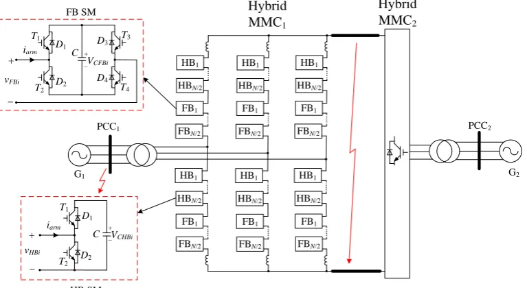
Fig. 1. Point-to-point HVDC link with hybrid MMCs
HB1
HBN/2
FB1
FBN/2
FBN/2
HBN/2
HB1
G1
PCC1
Hybrid
MMC1
Hybrid
MMC2
FB1
HB1
HBN/2
FB1
FBN/2
FBN/2
HBN/2
HB1
FB1
HB1
HBN/2
FB1
FBN/2
FBN/2
HBN/2
HB1
FB1
G2
PCC2
C + –VCFBi
T1 D1
T2 D2
T3 D3
T4 D4 iarm
+
_ vFBi
C T1
T2 D1
D2 iarm
+
_ vHBi
+ –VCHBi
Technology Copyright. The copy of record is available at IET Digital Library.
3 2. Accelerated Switching Function Model of Hybrid
MMCs
By combining FB and HB SMs in each arm, the hybrid MMC as shown in Fig. 1 is capable of blocking a DC fault and is an attractive option for HVDC application [22, 24]. By introducing the switching functions in active control and blocking states, the SFM of hybrid MMC is derived in this section.
2.1. Switching Functions of the FB and HB SMs
2.1.1. During Actively Control of the Hybrid MMC
During active control (not blocked), each FB and HB SM can generate three and two voltage levels respectively, and thus their switching functions are defined as:
1 3 2 4 2 4 1 3
1 4 2 3
2 3 1 4
0, , : ; , : , : ; , :
1, , : ; , :
1, , : ; , :
FBi
T T on T T off or T T on T T off
s T T on T T off
T T on T T off
(1)
2 1
1 2
0, : ; :
1, : ; :
HBi
T on T off
s
T on T off
(2)
where sFBi and sHBi are the switching functions of the ith FB and HB SMs, respectively; and the subscripts FB and HB denote the FB and HB SMs respectively.
From the switching functions defined by (1) and (2), each SM capacitor voltage of the proposed SFM can be calculated. Base on the trapezoidal integration, the current capacitor voltages VCFBi(t) and VCHBi(t) for the FB and HB stacks are obtained by adding the capacitor voltage variation ΔVC(t) to the previous value VCFBi(t-Δt) and VCHBi(t-Δt), considering the switching function sFBi and sHBi:
.CFBi CFBi FBi C
V t V t t s V t (3)
.CHBi CHBi HBi C
V t V t t s V t (4)
In each arm, the FB and HB SM capacitors in the current path are charged or discharged by the same arm current, and thus have the same capacitor voltage variation ΔVC(t):
1
2 arm arm C
i t i t t
V t t
C
(5)
where C is the SM capacitance and Δt is the simulation step. The total switching function stotal is obtained by rounding the product of the arm modulation index marm and the
SM number per arm N:
1 1
FB HB
N N
total FBi HBi arm
i i
FB HB arm
s s s round Nm
round N N m
(6)
where NFB and NHB are the respective FB and HB SM numbers per arm. Equation (6) determines the SM number inserted into the current path and discretizes the arm voltage of the SFM.
In the event of a pole-to-pole DC fault at the HVDC network, the DC voltage drops to almost zero. In order to operate the hybrid MMC on STATCOM mode, the required marm and stotal as shown in (6) could be less than zero. This indicates the FB SMs need to be inserted in the current path in negative polarity. The negative voltage generating capability of the hybrid MMC can be accurately reproduced by the proposed model, as will be discussed in Section 3.2.
2.1.2. In Blocking State of the Hybrid MMC
Alternatively, the hybrid MMC can be blocked during a DC fault. Immediately following the blocking of the MMC after the DC fault, the existing fault current in the arm charges the FB SM capacitors for both current directions as illustrated in Fig. 2 (a1) and (b1). In contrast, as shown in Fig. 2 (a2) and (b2), the HB SM capacitors are only charged by the positive arm current while the negative arm current flows through the antiparallel diode D2, where positive arm current iarm is defined as flowing from the top to the bottom.
[image:3.595.43.290.232.311.2]
a b
Fig. 2. Fault current path after the SMs are blocked, where the arm current iarm flowing from the top to the bottom is defined as
positive
a Positive arm current b Negative arm current
After the SMs are blocked, the arm currents may charge the SM capacitors, as illustrated in Fig. 2. The proposed model calculates the capacitor voltages of each SM according to (3) and (4) where the switching function is considered. When the hybrid MMC is blocked, the firing pulses of all the IGBTs in
the SMs are set at zero. Therefore, the aforementioned potential charging of the SM capacitors in blocking state cannot be represented and the capacitor voltages would remain unchanged if all the switching functions sFBi and sHBi in the blocking state are simply set as zero. To consider the potential C +
–VCFBi
T1 D1
T2 D2
T3 D3
T4 D4 iarm
+
_ vFBi full-bridge
(FB) SM
(a1)
C + –VCFBi
T1 D1
T2 D2
T3 D3
T4 D4 iarm
+
_ vFBi
(b1)
C T1
T2 D1
D2 iarm
+
_ vHBi
+ –VCHBi half-bridge
(HB) SM
(a2)
C T1
T2 D1
D2 iarm
+
_ vHBi
+ –VCHBi
Technology Copyright. The copy of record is available at IET Digital Library.
4 charging, equivalent switching functions in blocking state are
defined to accurately calculate the SM capacitor voltage using (3) and (4) as:
11 22 33 44
1, , , , : & 0
1, , , , : & 0
arm FBi
arm
T T T T off i
s
T T T T off i
(7)
1 2
1 2
1, , : & 0
.
0, , : & 0
arm HBi
arm
T T off i
s
T T off i
(8)
By considering the equivalent switching function, the potential charging of the SM capacitors during the blocking states is fully represented. Thus, the proposed SFM can precisely represent the SM capacitor voltage variations. This significantly improves the model accuracy compared to other alternatives, as will be demonstrated in Section 4.3.
2.2. Semiconductor Forward Voltage Drop of the SMs
The resistance of the off-state IGBT/diode Roff is very high and is normally in the range of several hundreds kΩ [3]. Table 1 lists the parameters of a 4.5kV/1200A IGBT from MITSUBISHI ELECTRIC [25]. The equivalent internal resistances (RonIGBT and RonD) and threshold voltages (V0IGBT and
V0diode) are derived by linearizing the on-state characteristic curves provided in the datasheets.
Table 1 Typical parameters of a 4.5kV/1200A IGBT for HVDC application
PARAMETER Value
IGBT internal resistance RonIGBT 1.8mΩ
threshold voltage V0IGBT 1.6V
Diode internal resistance RonD 0.9mΩ
threshold voltage V0diode 1.2V
Off-state resistance Roff 280kΩ
With the off-state IGBT considered as an open circuit (Roff=infinite), the semiconductor forward voltage drop of the SMs can be easily derived. The exact IGBT or anti-parallel diode which carries the arm current depends on the arm current polarity and the SM output voltage level. For the ith FB and HB SMs, the forward voltage drops VfdFBi and VfdHBi are calculated as
0 0
0 0
0 0
0
2 2 , 1, 0
2 2 , 1, 0
, 0, 0
, 0, 0
2 2 , 1, 0
2
onD arm D FBi arm
onIGBT arm IGBT FBi arm
onD onIGBT arm D IGBT FBi arm fdFBi
onD onIGBT arm D IGBT FBi arm
onIGBT arm IGBT FBi arm
on
R i t V s i t
R i t V s i t
R R i t V V s i t
V
R R i t V V s i t
R i t V s i t
R
2 0 , 1,
0D armi t VD sFBi iarm t
(9)
0
0
0
0
, 1, 0
, 1, 0
.
, 0, 0
, 0, 0
onD arm D HBi arm
onIGBT arm IGBT HBi arm fdHBi
onIGBT arm IGBT HBi arm
onD arm D HBi arm
R i t V s i t
R i t V s i t
V
R i t V s i t
R i t V s i t
(10)
By considering the actual conducting semiconductor devices, their forward voltage drops are more accurately reproduced by (9) and (10).
2.3. Generated Arm Voltage in the Proposed SFM
When the hybrid MMC is actively controlled, the voltage vFB and vHB generated by the FB and HB stacks in the proposed model are then derived from the aforementioned switching functions, SM capacitor voltages, and semiconductor forward voltage drops:
1 1
FB FB
N N
FB FBi FBi CFBi fdFBi
i i
v v s V V
(11)
1 1
HB HB
N N
HB HBi HBi CHBi fdHBi
i i
v v s V V
(12)where vFBi and VCFBi are the output and SM capacitor voltages of the ith FB SM, respectively; v
HBi and VCHBi are the output and capacitor voltages of the ith HB SM, respectively. During active control of the hybrid MMC, the contribution of the SM capacitor voltages VCHBi and VCFBi to vFB and vHB depends on the switching functions sFBi and sHBi. When the hybrid MMC is blocked, the reference voltages vFB and vHB are independent to the equivalent switching functions defined in (7) and (8) and all the FB and HB SM capacitor voltages VCHBi and VCFBi are added to vFB and vHB respectively:
1 1
FB FB
N N
FB FBi CFBi fdFBi
i i
v v V V
(13)
1 1
.
HB HB
N N
HB HBi CHBi fdHBi
i i
v v V V
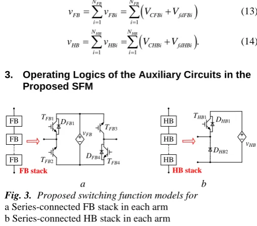
(14)3. Operating Logics of the Auxiliary Circuits in the Proposed SFM
[image:4.595.306.555.57.123.2]
a b
Fig. 3. Proposed switching function models for a Series-connected FB stack in each arm
b Series-connected HB stackin each arm
In each arm of the MMC, each of the FB and HB stacks, which are composed of hundreds SMs connected in-series, are represented by equivalent voltage sources vFB and vHB connected with the auxiliary circuit in the proposed model, as illustrated in Fig. 3, to simulate the current path in normal operation and during faults. The auxiliary circuit is composed
vFB
TFB1 DFB1
TFB2
TFB3
TFB4 DFB4 FB
FB FB
FB stack
vHB
THB1 D HB1
DHB2 HB
HB HB
[image:4.595.58.291.91.159.2] [image:4.595.299.554.415.639.2]Technology Copyright. The copy of record is available at IET Digital Library.
5 of IGBTs TFB1-TFB4 and diodes DFB1 and DFB4 for the FB stack
model; and IGBTs THB1 and diodes DHB1 and DHB2 for the HB stack model, as shown in Fig. 3 (a) and (b) respectively. The switching logics of the auxiliary circuit will be discussed in this section.
3.1. Switching Logics of the Auxiliary Circuit in the Proposed SFM for HB Stack
The switching function model of the HB stack is derived from the AMs in [7] and [22] but has the capability of
representing the voltages of each SM capacitor. As the HB SMs do not generate negative voltage, the voltage vHB produced by the HB SM stack, in Fig. 3 (b), is always greater than or equal to zero. The switching logics of the auxiliary circuit in the SFM for HB stack is governed by
1
1
: during active control
.
: , in blocking state
HB HB T on T off (15)
a
b c d e
Fig. 4. Arm current paths of the proposed SFM for HB stack, FB stack, and hybrid MMC in each arm respectively a Actively controlled with positive arm current
b Actively controlled with negative arm current c Blocking state with positive fault current d Blocking state with negative fault current e High impedance state
When the converter is actively controlled, the IGBT THB1 for the HB stack in Fig. 3 (b) is always on, allowing the arm current to flow in both positive and negative directions through the IGBT THB1 or its antiparallel diode DHB1, as shown in Figs. 4 (a1) and (b1) respectively, while diode DHB2 is reverse biased.
As the HB SMs do not have DC fault blocking capability, the fault current from the AC grid flows through the SM antiparallel diodes (negative arm current) into the DC fault after the blocking of the MMC. This is represented by turning off the IGBT THB1 and the fault current is allowed to flow through diode DHB2 from the AC to the DC side, Fig. 4 (d1). As shown in Fig. 4 (c1), the positive fault current flows through the antiparallel diode DHB1 and charges the voltage source vHB,
which can be depicted by (4) and (8). This is identical to the current path when the converter is actively controlled with positive arm current, Fig. 4 (a1), although they have opposite switching logics for the auxiliary circuit.
3.2. Switching Logics of the Auxiliary Circuit in the Proposed SFM for FB Stack
From the model of the HB SM stack shown in Fig. 3 (b), an alternative model for the FB stack is derived, as illustrated in Fig. 5 (a), which can represent the behaviour of the FB stack, except the negative voltage generating capability during active control. To continuously operate the hybrid MMC in STATCOM mode under a DC fault, the FB stack needs to generate negative voltage. Thus, the generated voltage vFB in vHB
THB1 D HB1
DHB2 iarm 1 SFM for HB stack (a1) vHB
THB1 D HB1
DHB2 iarm
1
(b1)
vHB
THB1 D HB1
DHB2 iarm
0
(c1)
vHB
THB1 D HB1
DHB2 iarm
0
(d1)
vHB
THB1 D HB1
DHB2
0
(e1)
vFB
TFB1 DFB1
TFB2
TFB3
TFB4 DFB4 iarm 1 0 1 0 SFM for FB stack (a2) vFB
TFB1 DFB1
TFB2
TFB3
TFB4 DFB4 iarm 1 1 0 0 (b2) vFB
TFB1 DFB1
TFB2
TFB3
TFB4 DFB4 iarm 0 1 0 1 (c2) vFB
TFB1 DFB1
TFB2
TFB3
TFB4 DFB4 iarm 0 1 0 1 (d2) vFB
TFB1 DFB1
TFB2
TFB3
TFB4 DFB4
0 0 1 1 (e2) FB stack iarm
TFB1 DFB1
TFB2
TFB3
TFB4 DFB4
THB1 DHB1
DHB2
HB stack vHB vFB 1 1 1 0 0 (a3) SFM for hybrid MMC FB stack
TFB1 DFB1
TFB2 TFB3
TFB4 DFB4
THB1 DHB1
DHB2
HB stack vHB vFB iarm 1 1 1 0 0 (b3) FB stack iarm
TFB1 DFB1
TFB2
TFB3
TFB4 DFB4
THB1 DHB1
DHB2
HB stack vHB vFB 0 0 0 1 1 (c3) FB stack
TFB1 DFB1
TFB2 TFB3
TFB4 DFB4
THB1 DHB1
DHB2
HB stack vHB vFB iarm 1 1 0 0 0 (d3) FB stack
TFB1 DFB1
TFB2 TFB3
TFB4 DFB4
THB1 DHB1
DHB2
Technology Copyright. The copy of record is available at IET Digital Library.
6 the proposed SFM for FB stack can be less than zero. This
results in the shoot-through of the diode pairs (DFB1, DFB2) and (DFB3, DFB4) for vFB < 0, as shown in Fig. 5 (b), where the shoot-through currents ist1 and ist2 are illustrated.
[image:6.595.53.268.101.163.2]
a b
Fig. 5. Alternative model without negative voltage representation
a Model for the FB stack in each arm
b Shoot-through of diode pairs (DFB1, DFB2) and (DFB3, DFB4) when vFB is negative
To avoid diode shoot-through, diodes DFB2 and DFB3 are replaced by IGBTs TFB2 and TFB3 in the proposed model, as shown in Fig. 3 (a). TFB2 and TFB3 act in the manner similar to ideal switches used in the MMC modeling in [9, 10], but with unidirectional current flow. The IGBT switching logics of the proposed model for FB stack are
1 4 2 3
1 4 2 3
, : , , : , during active control
.
, : , , : , in blocking state
FB FB FB FB
FB FB FB FB
T T on T T off
T T off T T on
(16)
When the MMCs are actively controlled (not blocked), the switches TFB1 and TFB4 are always on while TFB2 and TFB3 are turned off. Thus the arm currents can flow in both positive and negative directions through the antiparallel diodes DFB1 and DFB4 or the IGBTs TFB1 and TFB4, as illustrated in Figs. 4 (a2) and (b2). The voltage stresses on IGBTs TFB1 and TFB4 are zero, and TFB2 and TFB3 support the voltage vFB with both positive and negative polarities. The shoot-through issue illustrated in Fig. 5 (b) is thus avoided. The negative voltage capability of the proposed model, thereby the continuous operation in STATCOM mode, will be presented in Section 4.3.
The blocking of the MMCs after a fault is represented by turning off the IGBTs TFB1 and TFB4 and activating TFB2 and TFB3 in the proposed model. The positive fault current flows through the antiparallel diodes DFB1 and DFB4 and charges the equivalent voltage source vFB, as shown in Fig. 4 (c2). Although the switching logics for the auxiliary circuit are opposite, the current path in Fig. 4 (c2) is identical to that in Fig. 4 (a2). In Fig. 4 (d2), the negative fault current also charges the voltage source vFB through TFB2 and TFB3 and gradually drops. After the fault currents are suppressed to around zero (only leakage currents exist), the system operates in the high impedance mode [26, 27], as illustrated in Fig. 4 (e2) (none of the devices are ON).
The proposed model provides all the possible current paths as in a real MMC during active control and blocking mode and thus can be used to analyze the MMC behaviour under fault conditions.
3.3. Proposed SFM for the Hybrid MMC
Combining the SFMs for FB and HB stacks, the current paths for each arm of the hybrid MMC are shown in Figs. 4 (a3-e3). From (11) and (12), the generated arm voltages of the
hybrid MMC, varm, during active control and in the blocking state are
1 1
FB HB
N N
arm FB HB FBi CFBi fdFBi HBi CHBi fdHBi
i i
v v v s V V s V V
(17)
1 1
.
FB HB
N N
arm FB HB CFBi fdFBi CHBi fdHBi
i i
v v v V V V V
(18)As aforementioned, both the internal resistance and threshold voltage of the semiconductors in each SM are considered when calculating the reference voltages vFB and vHB, as depicted by (9) and (10). Thus, these parasitic parameters of the IGBTs and diodes in the auxiliary circuit do not need to be considered again, i.e. IGBTs THB1 and TFB1-TFB4, and diodes DHB1, DHB2, DFB1, and DFB4 are set in the manner similar to ideal devices.
In the simulation platform of the MATLAB/Simulink, snubber circuits are usually connected to the semiconductor devices in parallel to avoid spikes during switching transients. A pure resistive snubber circuit is adopted for the IGBTs and diodes in the auxiliary circuit (TFB1-TFB4, THB1, DFB1, DFB4, DHB1, and DHB2) where the snubber resistance Rs is properly set to represent the high impedance state of the SMs in the hybrid MMC, as:
1
2 .
s off
R R N (19)
With the off-state resistance Roffof 280kΩ as listed in Table 1, the peak of the leakage arm current for the simulated full-scale HVDC link (with the parameters detailed in Table 2) is around 10mA which is represented by the snubber circuit in the proposed MMC model.
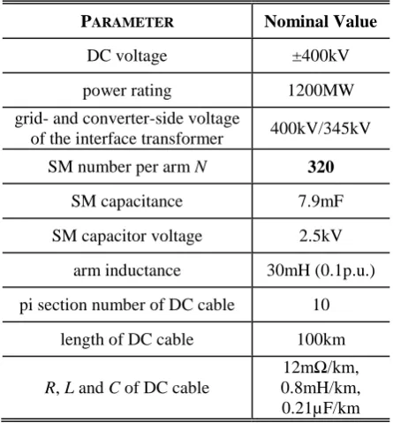
Table 2 Nominal parameters of the test full-scale HVDC link
in Fig. 1
PARAMETER Nominal Value
DC voltage ±400kV
power rating 1200MW
grid- and converter-side voltage
of the interface transformer 400kV/345kV
SM number per arm N 320
SM capacitance 7.9mF
SM capacitor voltage 2.5kV
arm inductance 30mH (0.1p.u.)
pi section number of DC cable 10
length of DC cable 100km
R, L and C of DC cable
12mΩ/km, 0.8mH/km, 0.21µF/km
As discussed in [26], the numerical oscillation only exists in the hard coded model (Model 2) which uses written codes to depict the complicated conduction and blocking states vFB
DFB1
DFB4 DFB2
DFB3 v
FB
ist1 DFB1
DFB4 DFB2
DFB3
ist2
1
[image:6.595.318.541.434.674.2]Technology Copyright. The copy of record is available at IET Digital Library.
7 of diodes. Such issue is not reported for the models which use
IGBTs/diodes to reproduce the fault current paths [10, 26]. Similarly, the potential conduction of diodes in blocking state is implemented using auxiliary circuits in the proposed model, avoiding the numerical oscillation problems seen in Model 2 in [26]. In addition, as presented in [26], the simulation speed of the hard coded model (Mode 2) is slower than Mode 3 which also adopts diodes to represent the fault current paths, due to the complicated codes of Mode 2.
4. Validation of the Proposed SFM
The presented SFM for hybrid MMC is assessed using the point-to-point HVDC link shown in Fig. 1. The simulation tool for this study is the Simscape/SimPowerSystems in the
R2016a 64-bit MATLAB/Simulink® environment. The
[image:7.595.308.550.141.348.2]down-scale 25-level (24 SMs per arm), 40MW / ±12kV system with parameters listed in Table 3 is simulated using both detailed switching model and the proposed SFM for accuracy and simulation speed validation. A full-scale 321-level system with parameters listed in Table 2 is also simulated. The HB and FB SM numbers NFB and NHB are both set at N/2 to successfully block the DC fault.
Table 3 Nominal parameters of the test down-scale HVDC link
in Fig. 1
PARAMETER Nominal Value
DC voltage ±12kV
power rating 40MW
grid- and converter-side voltage
of the interface transformer 16kV/13.2kV
SM number per arm N 24
SM capacitance 22.2mF
SM capacitor voltage 1kV
arm inductance 1.4mH (0.1p.u.)
pi section number of DC cable 10
length of DC cable 10km
R, L and C of DC cable 5mΩ/km, 0.2mH/km,
0.22µF/km
The arm inductance is set at 0.1p.u. to limit the circulating currents and the fault current rising rate [28, 29]. The IGBTs rated at 4.5kV are normally operated at around 2.5kV in HVDC application and thus 320 SMs are required per arm for the full-scale ±400kV HVDC system [25, 30]. The AC voltage rating of 400kV is standard for the high voltage grid in the UK and is thus adopted in this paper [31]. The DC cable parameters are based on the datasheets of cable manufacturers (ABB [32] and NKT Cables [33]) and the literatures of [30, 34].
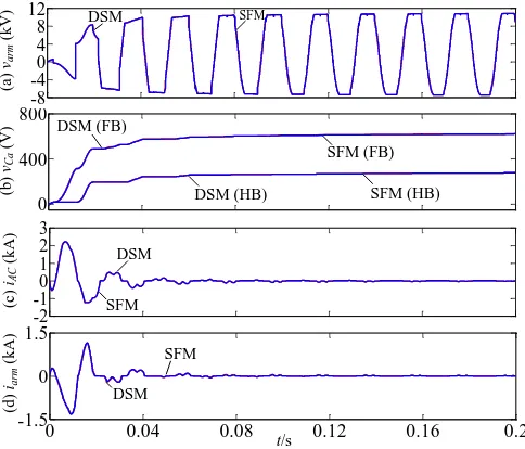
4.1. Pre-charging of Hybrid MMC using the Down-scale System
[image:7.595.40.292.347.579.2]The blocking state of the hybrid MMC is tested in the uncontrolled pre-charging scenario first, where all the SM capacitor voltages are initially set at zero and the hybrid MMC is blocked. To limit inrush currents, as a common practice, resistors of 3Ω are inserted between the transformer and the converter. Fig. 6 compares the simulated pre-charging process for the DSM and SFM using the down-scale 25-level system.
Fig. 6. Comparison of the pre-charging of the hybrid MMC with 25 levels using DSM and SFM
a Arm voltages
b FB and HB SM capacitor voltages c AC currents
d Arm currents
In addition to the positive voltage, the hybrid MMC arm also produces negative voltage during the uncontrolled charging process depending on the current direction of the FB SMs, Fig. 6 (a). The FB SM capacitors are charged by both positive and negative currents whereas the HB SM capacitors can only be charged by positive currents and are bypassed when the arm currents are negative. This leads to imbalanced charging between the FB and HB SM capacitors, as shown in Fig. 6 (b). The sequentially controlled charging method presented in [35] could be used to achieve equal charging of capacitors for the hybrid MMC. Nevertheless, the results of the proposed model match that of the detailed switching model (with almost identical results) and the uncontrolled charging process of the hybrid MMC is accurately represented by the SFM, as displayed in Fig. 6.
4.2. Startup of Hybrid MMC using the Full-scale System
The performance of the proposed SFM is also assessed using the aforementioned full-scale system with 321-level hybrid MMCs. For illustration purpose, all the capacitor voltages are initially set at the rated value and the active power is fast ramped from zero to 1p.u. in the duration of (0-0.1s). Close match is observed in Fig. 7 and the proposed model can reproduce the startup process of the hybrid MMC.
0 400 800
-2 -1 0 1 2 3
0 0.04 0.08 0.12 0.16 0.2
-1.5 0 1.5 -8 -4 0 4 8 12
SFM (FB)
DSM SFM
DSM
SFM
DSM SFM
t/s
(a
)
varm
(
k
V
)
(b
)
vCa
(
V
)
(c
)
iAC
(
k
A
)
(d
)
iarm
(
k
A
)
DSM (FB)
Technology Copyright. The copy of record is available at IET Digital Library.
[image:8.595.44.285.57.260.2]8
Fig. 7. Comparison of the startup of the hybrid MMC with 321 levels using DSM and SFM
a AC currents b Arm currents c DC currents
d Total capacitor voltages in an arm
4.3. Normal Operation using the Down-scale System
In this simulation, the hybrid MMC2 regulates the DC
voltage while MMC1 initially imports the rated 40 MW power
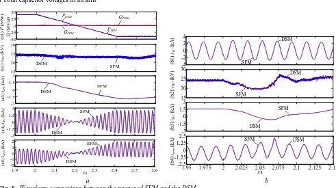
from G1 to the DC link with unity power factor. During t =2-2.4s, the power flow direction is reversed with the change rate of active power being -200MW/s. The comparison between the detailed switching model and the proposed model is presented in Fig. 8 (a), where close match is observed for all the waveforms. This validates that the proposed SFM can fully reproduce the dynamic behaviour of the hybrid MMC during power reversal.
4.4. AC Fault Scenario using the Down-scale System
The simulated scenario assumes a temporary three-phase-to-ground fault is applied on the AC-side of hybrid MMC1, as shown in Fig. 1, at t0=2s and is cleared after 60ms. Both stations keep operating during the AC fault.
Fig. 8 (b) compares the detailed switching model and the proposed SFM for the down-scale HVDC link. It can be seen that the proposed model again provides a highly accurate representation of the transients of the hybrid MMC during the AC fault.
[image:8.595.44.535.329.604.2]
a b
Fig. 8. Waveform comparison between the proposed SFM and the DSM
a During power reversal initiated at t0=2s: (a1) active and reactive power, (a2) DC voltages, (a3) DC currents, (a4) AC currents, and (a5) arm currents
b Under a three-phase-to-ground fault occurred at t0=2s: (b1) AC currents, (b2) DC voltages, (b3) DC currents, and (b4) arm currents
4.5. DC Fault Operating Condition
After the DC fault, the hybrid MMC can be deactivated to block the fault. Alternatively, the hybrid MMC can also continue operating during the fault as the FB SMs
can generate negative voltages. These two operations will be assessed in this subsection using the proposed SFM to validate its effectiveness for the DC fault studies.
-2.5 0 2.5 -2 -1 0 1 -1.5 0 1.5 3
0 0.04 0.08 0.12 0.16 0.2
700 800 900 DSM SFM DSM SFM DSM SFM DSM SFM t/s (b )
iarm
( k A ) (a )
iAC
( k A ) (c )
iDC
( k A ) (d )
vCa
T o ta l ( k V )
1.9 2 2.1 2.2 2.3 2.4 2.5 2.6
-2 -1 0 1 2 -50 -25 0 25 50 15 20 25 30 -3 -1.5 0 1.5 3 -3 -1.5 0 1.5 3
PDSM QDSM
QSFM PSFM
DSM SFM DSM SFM DSM SFM t/s DSM SFM (a 2 )
vDC
( k V ) (a 1 ) P (M W ) Q ( M V ar ) (a 3 )
iDC
( k A ) (a 4 )
iAC
( k A ) (a 5 )
iarm
( k A ) -4 -2 0 2 4 15 20 25 30 -3 -1.5 0 1.5 3
1.95 1.975 2 2.025 2.05 2.075 2.1 2.125 2.15
-2.5 -1.25 0 1.25 2.5 DSM SFM DSM SFM DSM SFM DSM SFM t/s (b 2 ) vD C ( k V ) (b 1 )
iAC
( k A ) (b 3 )
iDC
( k A ) (b 4 )
iarm
(
k
A
Technology Copyright. The copy of record is available at IET Digital Library.
9
4.5.1. Blocking the Hybrid MMC during the Fault using the Down-scale System
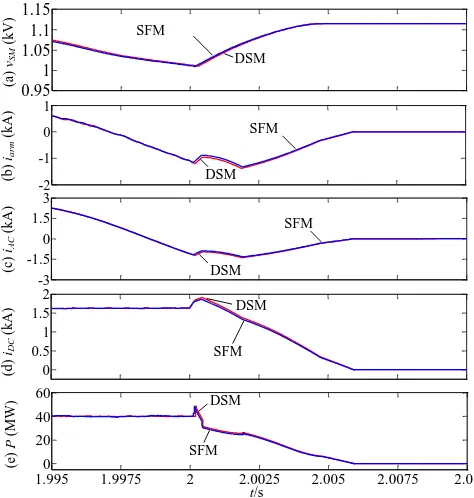
[image:9.595.311.555.52.407.2]After the fault detection, the converters are blocked. The FB SM capacitors are then charged by both positive and negative arm currents while the HB SM capacitors are only charged by the positive arm current (from the top to the bottom), as previously shown in Figs. 4 (c3) and (d3). Due to the introduction of the equivalent switching functions (equation (7) and (8)) in the proposed SFM after the MMC is blocked, the potential charging of the capacitors for both the FB and HB SMs are accurately represented.
Fig. 9. Comparison between the proposed SFM and the
DSM, where the pole-to-pole DC fault occurs at t0=2s and
the MMC is blocked after the fault a Average SM capacitor voltages b Arm currents
c AC currents d DC currents e Active power
Fig. 9 (a) compares the proposed SFM and the DSM for the down-scale 25-level HVDC link. The system is subjected to a permanent pole-to-pole DC fault at the middle
of the DC cable at t0=2s and the hybrid MMCs are blocked
after fault detection. As demonstrated in Fig. 9 (a), the waveforms of the proposed model match that of the detailed model before and after the blocking of the converter.
4.5.2. Continuous Operation of the Hybrid MMC during the DC Fault using the Full-scale System
The proposed SFM during continuous operation is assessed using the full-scale 321-level HVDC system with the parameters listed in Table 2. In the pre-fault condition, hybrid MMC1 imports 540MW active power from G1 and exchanges 430MVar (inductive) at its AC side with G1, while
MMC2 is set to maintain the DC voltage constant at ±400kV.
The DC fault occurs at t0=2s and the converter continues operating and provides reactive support for the AC grid.
Fig. 10. Waveforms of the proposed SFM for the 321-level hybrid MMC, where the pole-to-pole DC fault occurs at
t0=2s and the MMC remains operational after the fault
a DC voltage b DC current
c Active and reactive power d AC currents
e Arm voltages f Arm currents
g SM capacitor voltages
As the FB SMs have negative voltage generating capability, Fig. 10 (e), the hybrid MMC keeps operating although the DC voltage drops to around zero, Fig. 10 (a). Thus, the reactive power change between the AC and DC sides is controlled while the active power is decreased to zero (STATCOM mode), Fig. 10 (c). The AC side currents are also well regulated and the arm currents only experience small disturbance, as displayed in Fig. 10 (d) and (f). The proposed model can reproduce the capacitor voltage variation of each SM for the full-scale hybrid MMC with hundreds of SMs per arm, as shown in Fig. 10 (g). With the sorting algorithm presented in [36-38], the SM capacitor voltages are balanced during the ride-though operation and there are no extra requirements for the SM capacitor voltage balancing in the continuous operation of the hybrid MMC during a DC fault. The proposed SFM is capable of simulating high frequency behaviour during a fault and obtain satisfactory simulation accuracy. This is achieved with the typical SM capacitance requirement of 30-40kJ/MVA as suggested by ABB in [39], which yields a capacitor voltage ripple in the range of ±10% [40-44], as shown in Fig. 10 (g) . In contrast,
0.95 1 1.05 1.1 1.15
-2 -1 0 1
-3 -1.5 0 1.5 3
0 0.5 1 1.5 2
1.995 1.9975 2 2.0025 2.005 2.0075 2.01
0 20 40 60
(b
)
iarm
(
k
A
)
(a
)
vSM
(
k
V
)
(c
)
iAC
(
k
A
)
t/s
(d
)
iDC
(
k
A
)
(e
)
P
(
M
W
)
SFM
DSM
SFM
DSM
SFM
DSM
SFM DSM
SFM DSM
-2 -1 0 1 2
-200 0 200 400 600
(b
)
iDC
(
k
A
)
(a
)
vDC
(
k
V
)
(d
)
iAC
(
k
A
)
(f
)
iarm
(
k
A
)
(e
)
varm
(
k
V
)
(g
)
vSM
(
k
V
)
P
(c
)
P
(M
W
)
Q
(
M
V
ar
)
-300 0 300 600 900
-2 -1 0 1 2
-400 0 400 800
-1.5 0 1.5
1.95 2 2.05 2.1 2.15 2.2
2.2 2.4 2.6 2.8
Q
[image:9.595.45.282.187.436.2]Technology Copyright. The copy of record is available at IET Digital Library.
10 the average model in [2] is only valid when the SM
[image:10.595.43.287.167.245.2]capacitance is large enough to maintain near constant SM capacitor voltage. According to the switching function, the capacitor voltages of all the SMs are considered in the proposed SFM, as shown in Fig. 10 (g), leading to higher simulation accuracy.
Table 4 Simulation speed comparison of the proposed SFM
and other alternatives
Output Phase Voltage Level
Running Time (s)
DSM Model in
[10]
Proposed SFM
25 1,021 26 22
321 282,780
(estimated) 65 41
4.6. Simulation Speed Comparison
In addition to the higher accuracy, the proposed SFMs for hybrid MMC significantly accelerate the simulation speed. Two seconds of simulation is simulated in the
MATLAB/Simulink® software package with a simulation
step of 5µs, based on the Microsoft Windows 7 Enterprise platform with Intel Core i7 CPU @3.4GHz and 16GB RAM. For the down-scale 25-level HVDC link, the running time is significantly reduced from 1021s for DSM to 22s for the proposed SFM, as listed in Table 4. For the full-scale 321-level system the running time is only 41s for a 2s simulation. As it is extremely time consuming to simulate the full DSM with 321-levels, only a very short simulation (0.2s) is conducted. Scaling the implemented simulation time to the expected time of 2s, the estimated running time of the detailed switching mode with 321-levels is over 78 hours. For the hybrid MMC with 25 levels, the proposed SFM has close run time with the model in [10], (22s and 26s respectively, Table 4). However, the proposed model is much faster than the model in [10] to simulate the system with 321 levels and the run time is significantly reduced by a third (from 65s to 41s) which can provide significant benefit when studying large HVDC networks involving many converter stations.
5. Conclusion
This paper proposes an accelerated switching function model (SFM) for the hybrid MMC, where auxiliary circuits are adopted to represent all the possible current paths. The proposed SFM can represent the negative voltage generating capability of the FB stack while avoids the shoot-through of the diodes. In addition, the switching functions of the FB and HB SM in the blocking states are introduced in the proposed SFMs to depict the potential charging of the SM capacitors by the fault current, after the MMCs are blocked. Thus, the proposed model accurately replicates the capacitor voltage variations of each SM, which significantly improves the model accuracy and simulation speed when compared to other existing models. Simulation results validate that the proposed SFM of the hybrid MMC can provide accurate representation of MMC behaviour during various operating conditions, including normal operation, AC fault, and DC fault, etc.
6. Acknowledgement
This study is supported in part by the State Key Laboratory of Alternate Electrical Power System with Renewable Energy Sources (Grant No. LAPS17010).
7. References
[1] D. C. Ludois and G. Venkataramanan, "Simplified Terminal Behavioral Model for a Modular Multilevel Converter," IEEE Trans. Power Electron., vol. 29, pp. 1622-1631, 2014.
[2] X. Jianzhong, A. M. Gole, and Z. Chengyong, "The Use of Averaged-Value Model of Modular Multilevel Converter in DC Grid," IEEE Trans. Power Del., vol. 30, pp. 519-528, 2015.
[3] F. B. Ajaei and R. Iravani, "Enhanced Equivalent Model of the Modular Multilevel Converter," IEEE Trans. Power Del., vol. 30, pp. 666-673, 2015.
[4] Y. Feng, L. Weixing, W. Xitian, and X. Da, "Fast
Voltage-Balancing Control and Fast Numerical
Simulation Model for the Modular Multilevel Converter," IEEE Trans. Power Del., vol. 30, pp. 220-228, 2015.
[5] W. Jun, R. Burgos, and D. Boroyevich, "Switching-Cycle State-Space Modeling and Control of the Modular Multilevel Converter," Emerging and Selected Topics in Power Electronics, IEEE Journal of, vol. 2, pp. 1159-1170, 2014.
[6] J. Peralta, H. Saad, S. Dennetiere, J. Mahseredjian, and S. Nguefeu, "Detailed and Averaged Models for a
401-Level MMC–HVDC System," IEEE
Transactions on Power Delivery, vol. 27, pp. 1501-1508,
2012.
[7] R. Li, L. Xu, L. Yao, and B. W. Williams, "Active Control of DC Fault Currents in DC Solid-State Transformers during Ride-Through Operation of
Multi-Terminal HVDC Systems," IEEE Transactions on
Energy Conversion, vol. PP, pp. 1-1, 2016.
[8] U. N. Gnanarathna, A. M. Gole, and R. P. Jayasinghe, "Efficient Modeling of Modular Multilevel HVDC Converters (MMC) on Electromagnetic Transient Simulation Programs," IEEE Trans. Power Del., vol. 26, pp. 316-324, 2011.
[9] F. Yu, W. Lin, X. Wang, and D. Xie, "Fast Voltage-Balancing Control and Fast Numerical Simulation Model for the Modular Multilevel Converter," IEEE Transactions on Power Delivery, vol. 30, pp. 220-228, 2015.
[10] H. Saad, K. Jacobs, W. Lin, and D. Jovcic, "Modelling of MMC including half-bridge and Full-bridge submodules for EMT study," in 2016 Power Systems
Computation Conference (PSCC), 2016, pp. 1-7.
[11] P. D. Judge, G. Chaffey, P. Clemow, M. M. Merlin, and T. C. Green, "Hardware testing of the alternate arm converter operating in its extended overlap mode," 2015. [12] F. J. Moreno, M. M. C. Merlin, D. R. Trainer, T. C. Green, and K. J. Dyke, "Zero phase sequence voltage injection for the alternate arm converter," in 11th IET International Conference on AC and DC Power Transmission, 2015, pp. 1-6.
Technology Copyright. The copy of record is available at IET Digital Library.
11 converter," in 13th IET International Conference on AC
and DC Power Transmission (ACDC 2017), 2017, pp.
1-6.
[14] E. Farr, R. Feldman, A. Watson, J. Clare, and P. Wheeler, "A sub-module capacitor voltage balancing scheme for the Alternate Arm Converter (AAC)," in Power Electronics and Applications (EPE), 2013 15th
European Conference on, 2013, pp. 1-10.
[15] W. Yeqi and R. Marquardt, "Future HVDC-grids employing modular multilevel converters and hybrid DC-breakers," in Power Electronics and Applications
(EPE), 2013 15th European Conference on, 2013, pp.
1-8.
[16] P. Clemow, P. Judge, G. Chaffey, M. Merlin, T. Luth, and T. C. Green, "Lab-scale experimental multilevel modular HVDC converter with temperature controlled cells," in Power Electronics and Applications
(EPE'14-ECCE Europe), 2014 16th European Conference on,
2014, pp. 1-10.
[17] R. Marquardt, "Modular Multilevel Converter topologies with DC-Short circuit current limitation," in Power Electronics and ECCE Asia (ICPE & ECCE), 2011 IEEE
8th International Conference on, 2011, pp. 1425-1431.
[18] R. Marquardt, "Modular Multilevel Converter: An universal concept for HVDC-Networks and extended DC-Bus-applications," in Power Electronics Conference
(IPEC), 2010 International, 2010, pp. 502-507.
[19] R. Li, J. E. Fletcher, L. Xu, D. Holliday, and B. W. Williams, "A Hybrid Modular Multilevel Converter With Novel Three-Level Cells for DC Fault Blocking Capability," IEEE Trans. Power Del., vol. 30, pp. 2017-2026, 2015.
[20] A. Nami, L. Jiaqi, F. Dijkhuizen, and G. D. Demetriades,
"Modular Multilevel Converters for HVDC
Applications: Review on Converter Cells and Functionalities," IEEE Trans. Power Electron., vol. 30, pp. 18-36, 2015.
[21] R. Zeng, L. Xu, L. Yao, and B. W. Williams, "Design and Operation of a Hybrid Modular Multilevel Converter," IEEE Trans. Power Electron., vol. 30, pp. 1137-1146, 2015.
[22] R. Zeng, L. Xu, and L. Yao, "DC/DC Converters Based on Hybrid MMC for HVDC Grid Interconnection," in AC and DC Power Transmission, 11th IET International Conference on, 2015, pp. 1-6.
[23] W. Li and J. Bélanger, "An Equivalent Circuit Method for Modelling and Simulation of Modular Multilevel
Converters in Real-Time HIL Test Bench," IEEE
Transactions on Power Delivery, vol. 31, pp. 2401-2409,
2016.
[24] R. Li, G. P. Adam, D. Holliday, J. E. Fletcher, and B. W. Williams, "Hybrid Cascaded Modular Multilevel Converter With DC Fault Ride-Through Capability for the HVDC Transmission System," IEEE Trans. Power Del., vol. 30, pp. 1853-1862, 2015.
[25] Mitsubishi Electric Corp, CM1200HG-90R HVIGBT module datasheet, Jul 2013.
[26] H. Saad, S. Dennetiere, J. Mahseredjian, P. Delarue, X. Guillaud, J. Peralta, et al., "Modular Multilevel Converter Models for Electromagnetic Transients,"
IEEE Transactions on Power Delivery, vol. 29, pp.
1481-1489, 2014.
[27] T. Ould-Bachir, H. Saad, S. Dennetiere, and J.
Mahseredjian, "CPU/FPGA-based Real-Time
Simulation of a Two-Terminal MMC-HVDC System,"
IEEE Transactions on Power Delivery, vol. PP, pp. 1-1,
2015.
[28] Q. Tu, Z. Xu, Y. Chang, and L. Guan, "Suppressing DC Voltage Ripples of MMC-HVDC Under Unbalanced
Grid Conditions," IEEE Transactions on Power
Delivery, vol. 27, pp. 1332-1338, 2012.
[29] Q. Tu, Z. Xu, and L. Xu, "Reduced Switching-Frequency Modulation and Circulating Current Suppression for Modular Multilevel Converters," IEEE Transactions on
Power Delivery, vol. 26, pp. 2009-2017, 2011.
[30] R. Li, J. Fletcher, L. Xu, and B. Williams, "Enhanced Flat-Topped Modulation for MMC Control in HVDC Transmission Systems," IEEE Transactions on Power Delivery, vol. PP, pp. 1-1, 2016.
[31] R. Li, L. Xu, D. Holliday, F. Page, S. J. Finney, and B. W. Williams, "Continuous Operation of Radial Multiterminal HVDC Systems Under DC Fault," IEEE Transactions on Power Delivery, vol. 31, pp. 351-361, 2016.
[32] ABB Group, XLPE Land Cable Systems User’s Guide, 2006.
[33] NKT Cables, High Voltage Cable Systems Cables and Accessories up to 550kV.
[34] P. Bresesti, W. L. Kling, R. L. Hendriks, and R. Vailati, "HVDC Connection of Offshore Wind Farms to the Transmission System," IEEE Transactions on Energy Conversion, vol. 22, pp. 37-43, 2007.
[35] R. Zeng, L. Xu, L. Yao, and D. J. Morrow, "Precharging and DC Fault Ride-Through of Hybrid MMC-Based
HVDC Systems," IEEE Transactions on Power
Delivery, vol. 30, pp. 1298-1306, 2015.
[36] D. Fujin and C. Zhe, "A Control Method for Voltage Balancing in Modular Multilevel Converters," IEEE Trans. Power Electron., vol. 29, pp. 66-76, 2014. [37] Q. Jiangchao and M. Saeedifard, "Reduced
Switching-Frequency Voltage-Balancing Strategies for Modular Multilevel HVDC Converters," IEEE Trans. Power Del., vol. 28, pp. 2403-2410, 2013.
[38] S. Gum Tae, L. Hee-Jin, N. Tae Sik, C. Yong-Ho, L. Uk-Hwa, B. Seung-Taek, et al., "Design and Control of a Modular Multilevel HVDC Converter With Redundant Power Modules for Noninterruptible Energy Transfer,"
IEEE Trans. Power Del., vol. 27, pp. 1611-1619, 2012.
[39] B. Jacobson, P. Karlsson, G. Asplund, L. Harnefors, and T. Jonsson, "VSC-HVDC transmission with cascaded two-level converters," in Cigré session, 2010, pp. B4-B110.
[40] R. Li, L. Xu, and L. Yao, "DC Fault Detection and Location in Meshed Multiterminal HVDC Systems Based on DC Reactor Voltage Change Rate," IEEE
Transactions on Power Delivery, vol. 32, pp. 1516-1526,
2017.
[41] M. M. Merlin and T. C. Green, "Cell Capacitor Sizing in Multilevel Converters: Cases of the MMC and AAC," IET Power Electronics, vol. 1-21, 2014.
[42] J. Doerksen, "Design and Implementation of a Modular Multilevel Converter," University of Manitoba, 2013. [43] L. Lin, Y. Lin, Z. He, Y. Chen, J. Hu, and W. Li,
Technology Copyright. The copy of record is available at IET Digital Library.
12 Number," IEEE Transactions on Power Electronics, vol.
31, pp. 5369-5377, 2016.