Fully tuneable, Purcell-enhanced solid-state quantum emitters
M.Petruzzella,1,a)T.Xia,1F.Pagliano,1S.Birindelli,1L.Midolo,2Z.Zobenica,1L. H.Li,3 E. H.Linfield,3and A.Fiore1
1
COBRA Research Institute, Eindhoven University of Technology, P.O. Box 513, NL-5600MB Eindhoven, The Netherlands
2
Niels Bohr Institute, University of Copenhagen, Blegdamsvej 17, DK-2100 Copenhagen, Denmark
3
School of Electronic and Electrical Engineering, University of Leeds, Leeds LS2 9JT, United Kingdom
(Received 25 June 2015; accepted 28 September 2015; published online 8 October 2015)
We report the full energy control over a semiconductor cavity-emitter system, consisting of single Stark-tunable quantum dots embedded in mechanically reconfigurable photonic crystal membranes. A reversible wavelength tuning of the emitter over 7.5 nm as well as an 8.5 nm mode shift are realized on the same device. Harnessing these two electrical tuning mechanisms, a single exciton transition is brought on resonance with the cavity mode at several wavelengths, demonstrating a ten-fold enhancement of its spontaneous emission. These results open the way to bring several cavity-enhanced emitters mutually into resonance and therefore represent a key step towards scalable quantum photonic circuits featuring multiple sources of indistinguishable single photons.
VC 2015 AIP Publishing LLC. [http://dx.doi.org/10.1063/1.4932946]
Last decade has witnessed pioneering advancements in the development of the elementary building blocks for envisioned quantum photonic circuits,1 which may enable simulating problems, which are intractable on classical com-puters.2,3 Efficient on-demand single-photon sources, obtained by coupling a quantum emitter to an optical cavity, represent one of these key building blocks. Additionally, cavity quantum electrodynamics (c-QED) offers a viable solution to create a coherent and efficient interface between light and matter qubits, as needed to establish entanglement between distant quantum emitters via a photonic channel.4 Among its numerous solid-state implementations, quantum dots (QDs) embedded in semiconductor nano-resonators have emerged as one of the most promising integrated plat-forms,5,6specifically for the on-demand generation of single and entangled photons.7 Coupling to photonic crystal cav-ities (PCCs) is notably attractive due to their engineerable electromagnetic environment which provides record quality factors (Q) in a wavelength-scale volume.8Indeed, the basic c-QED phenomena have been recently demonstrated, includ-ing Rabi splittinclud-ing,9static10and dynamic11,12control of spon-taneous emission and single-photon non-linearities.13,14 Nevertheless, integrating and interconnecting multiple c-QED nodes within the same chip poses considerable scal-ability issues.
One of the leading experimental challenges in this con-text resides in the spectral matching of multiple cavity-emitter systems, which requires the deterministic control over the energy of both emitters and cavities. To this end, post-processing tuning strategies are imperative because of the QD inhomogeneous broadening and the intrinsic fabrica-tion imperfecfabrica-tions which spread the actual cavity resonance over several nanometers.
Lately, a number of techniques based on electric, mag-netic, temperature and strain control have been successfully employed to tune the emitters’ energy.5 On the other hand,
several proposals have been adopted to tune the cavity spectrum, including thermal methods,15 gas adsorption,16 photochromic materials,17 photo-oxidation,18 free carrier injection,19,20and nano-electromechanical systems.21–23
However, so far, the crucial goal of achieving a simulta-neous energy control of an integrated emitter and its cavity has not been attained yet. In this letter we present a fully tuneable cavity-emitter system, where both the cavity and emitter wavelengths can be independently controlled in the same semiconductor device. This enables the demonstration of Purcell-enhancement from an energy-tuneable single dot.
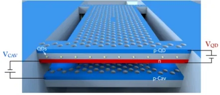
Our device is sketched in Figure1and incorporates two parallel photonic crystal membranes which can be vertically displaced by capacitive forces.22To this end, an n-i-p diode realized across the membranes provides the electrostatic actuation when it is operated in reverse bias. The resulting nano-mechanical displacement modifies the effective index of the coupled modes of the double-membrane waveguide, leading to a blue(red)-shift of the vertically anti-symmetric (symmetric) modes.24The QD region is grown in the middle of the top slab to remove any interaction with the electro-static field.23A second p-i-n diode, sharing the n-layer with the cavity-tuning diode, is fabricated on the top membrane to apply a vertical electric field across the QD layer. In such a
FIG. 1. (a) Sketch of the device illustrating the photonic crystal cavity pat-terned through two vertically coupled membranes. A top p-i-n diode realized across the top slab governs the QD energy via the quantum-confined Stark effect, while a second n-i-p diode controls the cavity resonance through capacitive forces.
a)
Electronic mail: [email protected]
[image:1.612.327.548.596.692.2]way, the emitter’s energy is tuned by the quantum-confined Stark effect.25
The sample is grown by molecular beam epitaxy and includes two GaAs slabs of equal thickness (170 nm) isolated by a 240-nm-thick sacrificial Al0:7Ga0:3As spacer. A 1.5l
m-thick Al0:7Ga0:3As layer separates the double membranes
from the undoped (001) GaAs substrate. Low-density InAs QDs are grown in the middle of the upper membrane in the Stranski-Krastanov mode at a very low growth rate.26 Additionally, two 17-nm-thick Al0:3Ga0:7As barriers are
introduced 8 nm above and below the QDs in order to sup-press the tunneling probability of electron-hole pairs out of the dot and consequently increase the exciton tuning range.27 The upper 50-nm thick region of both membranes is p-doped whereas the bottom 50-nm-thick part of the top slab is n-doped (pQD¼1:51018;n¼pcav¼21018cm3). The fabrication consists in the realization of the double diodes followed by the patterning of the photonic crystal structure. Employing two optical lithographic steps and selective wet etchings, vias to the p and n regions are opened and Ti/Au (50/200 nm) pads are evaporated on top of them. In this way, two p-i-n diodes sharing a common n-layer are realized in a single lift-off process. Together with the p-via, a flexible four-arm micro-bridge is also defined on the top membrane. A PCC created by three missing holes (lattice constant a¼395 nm and radius r¼0:31a) is defined on a 400-nm-thick Si3N4mask by 30 kV-electron beam lithography and a
reactive ion etching step. The radii and positions of the ten holes surrounding the defect region are modified to provide a theoretical quality factor Q¼34 000, as calculated by 3D finite-element modeling. Subsequently, the PCC is vertically transferred to both membranes by inductively coupled plasma etching. The release of the free standing structure is carried out by selectively removing the sacrificial layers via cold (1C) HCl solution while keeping the Si3N4 mask to
avoid sticking arising from capillary forces.22 Finally, the Si3N4layer is eliminated by isotropic O2-CF4plasma ashing.
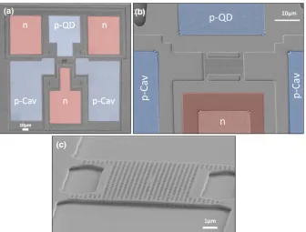
Figure2shows the scanning electron micrographs of the full device.
Low-temperature (T¼9 K) micro-photoluminescence
(lPL) experiments were performed in a continuous-flow helium cryostat equipped with two electrical probes sharing a common ground and approaching the sample from opposite directions. QDs were excited with an above-bandgap diode laser (k¼785 nm) and their emission was collected through the same objective (numerical aperture NA¼0:4) and ana-lyzed by a fiber-coupled spectrometer, after being spectrally isolated from the pump laser via a dichroic beam-splitter.
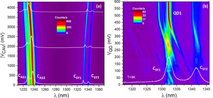
Figure 3(a) shows the color-coded lPL measurements acquired in the strong pumping regime (50lW measured before the objective) in order to probe the cavity modes while sweeping the voltage across the membranes. The spec-trum is dominated by four eigenmodes of the PCC cavity. By increasing the reverse bias across the membranes (VCAV), the two pairs of modes shift in wavelengths along opposite directions. This effect represents the unambiguous signature of the mechanical origin of the mode-tuning and rules out any possible thermal origin.
Here, a maximum and reproducible cavity shift of 8.5 nm is achieved at4.5 V, without reaching the irreversi-ble pull-in condition that brings the structure to collapse. In addition, from the tuning direction, we classify the high-energy modes as anti-symmetric (CAS1;CAS2) and two modes
situated around 1330 nm as symmetric (CSY1;CSY2). From a
[image:2.612.53.389.511.766.2]comparison with the spectrum calculated using a finite-element method, we attributed the anti-symmetric modes to lowest-order modes mainly polarized perpendicular to the cavity axis, while the symmetric lines have been identified as higher order-modes with dominant polarization along the cavity axis. The quality factor of these modes is around 1000, while quality factors up to 5000 have been measured on other devices on the same chip, showing that Q factors adequate for the enhancement of spontaneous emission are possible in the double-membrane structure.
In the following tuning experiments, we focus on the symmetric modeCSY1, which is located around the ground
state of the QDs. When this mode is shifted in frequency, a modulation of its quality factor is observed ranging from 620 to 900. The oscillation in the cavity losses can be related to the change in the amount of wave-vector components of the cavity field lying inside the light cone when the two slabs are brought closer.28
After reducing the laser power to the nW-level (80 nW), just below the saturation level of QDs, also single QD lines appear in the spectrum. Figure3(b)presents the QD tuning experiments carried out on the same device. Here, the color-coded image is built up from severall-PL spectra acquired while the Stark diode is operated in forward bias. When the voltage applied to the QD-diode is increased (in forward bias) from 0 to 0.6 V, the exciton transitions shift to the blue achieving a maximum tuning range of 7.5 nm. A clear enhancement of the spontaneous emission of single dot lines is observed when their energy crosses the cavity mode posi-tion. Remarkably, cavity modes are still visible in the config-uration where there is no QD matching their energy due to the pumping from multi-excitons transitions29,30 and phonon-assisted feeding mechanisms.31At negative bias the QD emission is suppressed suggesting that the built-in junc-tion field (Fbi¼ 200 KV=cm) is sufficient to sweep the carriers away from the active region. Besides, we observe the inhibition of the tuning close to the turn-on voltage of the diode (0.6 V) due to the increasing current. Consistently with previous reports on the quantum-confined Stark effect in InAs QDs,25 the blue shifting of single dot lines indicates that the electron wave function is located below the hole wave function with respect to the growth axis, giving rise to an inverted hole-electron alignment. From the fitting of the tuning curves, we estimated for the excitonic line QD1 a permanent dipole moment p¼ 0:1560:04enm and a polarizabilityb¼ 4:960:1103enm kV–1cm, compara-ble with previous works.12 The tuning rate is particularly high (14.4meV
V ) due to the thin intrinsic region (70 nm) of the Stark-diode.
The simultaneous control over the full emitter-cavity sys-tem is reported in Figure4. Here, a quantum dot line (QD1) is first spectrally positioned at k1¼1332:2 nm by applying a
Stark voltage ofVQD¼590 mV. In this situation, resonance with the cavity mode is obtained atVCAV¼0 V (Figure4(a)).
By changing the Stark field (VQD¼320 mV) the QD is
red-shifted at a second wavelength k2¼1334:5 nm
(Figure4(b)). The cavity can be brought again into resonance at a voltage VCAV¼ 1:4 V (Figure 4(b)). As shown in Figure4(c), the electrical control on the exciton line does not significantly affect the cavity mode position (Figure4(c)), de-spite the presence of an electro-optic effect in GaAs (the cal-culated electro-optic wavelength shift over the voltage range of Figure4(c)is 0.01 nm). However, when the cavity-diode is tuned from 0 to 1.6 V a crosstalk is observed on the QD-diode which results in a small blue-shift of the excitonic line QD1 by 0.4 nm (VQD¼320 mV) as reported in Figure4(d), whose origin is not understood. Additionally forjVCAVj ffi2:0 V, the mode tuning rate decreases and the QDs lines start red-shifting. We attribute this behavior to the increasing current flowing across the diodes. For a reverse cavity bias voltage
jVCAVj>2:0 V the current in the cavity diode was observed to strongly increase in the presence of a forward QD bias, which is indicative of the expected transistor behavior in this pinip junction. The corresponding temperature increase pro-duces the red-shift of the QD lines observed in Figure 4(d). Notwithstanding, for a range of energies spanning over 2.6 meV the wavelength-shift of QD lines is one order of magnitude less than the cavity tuning. This greatly facilitates the tuning of the entire quantum node fromk1tok2.
To further explore the QD-cavity coupling we investi-gated the temporal dynamics of the excitonic line QD1 in the
weak pumping regime.32 Time-resolved experiments are
performed employing an 80 MHz pulsed diode laser (k¼757 nm, average power P¼30 nW, pulse width¼70 ps) as excitation source, sending the PL emission through a tuna-ble band-pass filter (bandwidth¼0.5 nm) and making use of a superconducting single photon detector and a correlation card (PicoHarp300) to measure the photon arrival time. The full width at half maximum (FWHM) of the instrument response function (IRF) gives a temporal resolution of 90 ps.
The decay curves of the excitonic transition QD1 are reported in Figure5. When the quantum dot line is spectrally aligned with the cavity resonance atk1¼1332:2 nm (purple
dots,VQD¼590 mV,VCAV¼0 mV) and atk02¼1335:0 nm
(red dots, VQD¼300 mV, VCAV¼ 1600 mV), a decrease
of its radiative lifetime is visible compared to the case in which the dot is set at k1, off-resonance from the
cavity-mode atk02(blue dots).
[image:3.612.52.392.55.211.2]From a bi-exponential fit convoluted with the IRF we derive the on-resonance time constants of the fast decay
components related to cavity-enhanced single-QD emission
sONðk1Þ ¼140 ps;sONðk02Þ ¼190 ps. The slow decay com-ponentsON;Slowðk1Þ ¼960 ps is attributed to the residual
con-tribution of the background-pumped cavity mode emission, which has a measured time constant sMode ¼830 ps. The
experimental error bar is estimated as20 ps from the stand-ard deviation of values fitted from different measurements. In the off-resonance configuration the dot is characterized by a single exponential dynamics with time constant
sOFF¼1:0260:02 ns. The QD ensemble data set is shown
for comparison (green dots) and has a single decay constant
sBulk¼1:5560:02 ns, similar to previous reports from
simi-lar QDs.33
In general the actual decay rateCof a QD exciton in a PCC environment in the presence of an electric field can be
written as34 C¼CCAVþCLeakyþCnrðFÞ, where CCAV
rep-resents the Purcell-enhanced emission in the cavity mode,
CLeaky encodes the decay rate into the leaky modes of the
PCC, while Cnr accounts for the non-radiative processes
including tunneling of the electron out of the dot and depends on the applied electric field. However, within the low-field values used in this experiment (Fðk1Þ ¼ 135 kV/ cm and Fðk02Þ ¼ 167 kV/cm), both Cnr and the possible
modification of the oscillator strength are small.27Therefore, neglecting the decay channels not related to the presence of the cavity (CLeakyþCnr), estimated in theð56 nsÞ1range
from literature data of similar QD heterostructure,35we at-tribute the shortening of the on-resonance decay rate to the Purcell effect,36,37 quantifying a Purcell enhancement of
FPðk02Þ ¼
sONðk02Þ
sBulk ¼861 andFPðk1Þ ¼
sONðk1Þ
sBulk ¼1162 for the
two wavelengths. The difference in the spontaneous emis-sion enhancement at different wavelengths can be attributed to the modification of the quality factor when the cavity is tuned. Indeed, considering negligible the variation of the effective mode volume of the cavity (below 2% from
simulations) the ratio between Qðk1Þ ¼820630 and
Qðk02Þ ¼650630 is comparable to the ratio of the on-resonance decay times sONðk1Þ
sONðk02Þ¼
1:3560:34. We also note
that the observed decrease in decay time when tuning the QD-cavity system from k02 tok1cannot be explained by an
increase in the tunneling rate, since the electric field applied fork1is lower than the one fork02.
The suppression of the spontaneous emission off-resonance is hampered by the limited tuning range in this
experiment as confirmed by the ratio CCðkðkCAV¼kQD¼k1Þ
CAV¼k02;kQD¼k1Þ¼
1063 estimated from the spectral mismatchk1–k02¼2:8 nm,
using the expression in Ref. 38and taking into account the emission into leaky modes and non-radiative recombination processes.
[image:4.612.51.410.55.297.2]In conclusion, we have experimentally demonstrated a solid-state cavity-emitter system where both the energy of
FIG. 4. Electromechanical tuning of the cavity mode performed when two dif-ferent voltagesVQD¼590 mV (a) and VQD¼320 mV (b) are applied to the
QD diode. Resonant coupling between the modeCSY1and QD1 is achieved at k1¼1332:2 nm (VQD¼590 mV,VCAV ¼0 mV) and k2¼1334:5 nm
(VQD¼320 mV, VCAV¼ 1400 mV).
(c) and (d) The tuning curves for QD1 (red squares) andCSY1(blue dots) as a
function ofVQDandVCAV, respectively.
FIG. 5. Time-resolved normalized photoluminescence dynamics of the exci-tonic transition QD1 on resonance with the cavity mode at two distinct wavelengths,k1¼1332:2nm (purple dots) and k02¼1335nm (red dots).
The off-resonance decay histogram of the dot positioned atk1, while the
cavity wavelength is set atk0
2, is shown in blue. The QD ensemble evolution
[image:4.612.65.284.513.686.2]the emitter and the cavity resonance are independently and electrically controlled. By combining the Stark tuning of quantum dots with the nano-electromechanical actuation of the cavity the deterministic, reversible and real-time spectral alignment of the entire quantum node has been demon-strated. We studied the regime where the spontaneous emis-sion of single excitons can be modulated by one order of magnitude at several energies. The integration of this plat-form with ridge waveguides,39 needed to transfer photons with low losses on the chip, will open the way to multi-node integrated cavity-quantum electrodynamics experiments and therefore de facto to scalable quantum sources for integrated quantum photonics.
We acknowledge stimulating discussions with R. W. van der Heijden, S. Fattah poor, and C. Jin. This research
was financially supported by the Dutch Technology
Foundation STW, Applied Science Division of NWO, the Technology Program of the Ministry of Economic Affairs under Project Nos. 10380 and 12662 and by NanoNextNL, a micro and nanotechnology program of the Dutch Ministry of Economic Affairs, Agriculture and Innovation (EL&I) and 130 partners.
1
J. L. O’Brien, A. Furusawa, and J. Vucˇkovic´, Nat. Photonics 3, 687 (2009).
2
A. Aspuru-Guzik and P. Walther,Nat. Phys.8, 285 (2012).
3
S. Aaronson and A. Arkhipov, in Proceedings of the forty-third Annual ACM Symposium on Theory of Computing(ACM, 2011), pp. 333–342.
4
H. Kimble,Nature453, 1023 (2008).
5
S. Buckley, K. Rivoire, and J. Vucˇkovic´, Rep. Prog. Phys.75, 126503 (2012).
6
P. Lodahl, S. Mahmoodian, and S. Stobbe, Rev. Mod. Phys. 87, 347 (2015).
7
A. J. Shields,Nat. Photonics1, 215 (2007).
8
Y. Akahane, T. Asano, B.-S. Song, and S. Noda,Nature425, 944 (2003).
9T. Yoshie, A. Scherer, J. Hendrickson, G. Khitrova, H. Gibbs, G. Rupper,
C. Ell, O. Shchekin, and D. Deppe,Nature432, 200 (2004).
10
P. Lodahl, A. F. Van Driel, I. S. Nikolaev, A. Irman, K. Overgaag, D. Vanmaekelbergh, and W. L. Vos,Nature430, 654 (2004).
11
C.-Y. Jin, R. Johne, M. Y. Swinkels, T. B. Hoang, L. Midolo, P. J. van Veldhoven, and A. Fiore,Nat. Nanotechnol.9, 886 (2014).
12
F. Pagliano, Y. Cho, T. Xia, F. van Otten, R. Johne, and A. Fiore,Nat. Commun.5, 5786 (2014).
13
D. Englund, A. Faraon, I. Fushman, N. Stoltz, P. Petroff, and J. Vucˇkovic´,
Nature450, 857 (2007).
14I. Fushman, D. Englund, A. Faraon, N. Stoltz, P. Petroff, and J. Vucˇkovic´,
Science320, 769 (2008).
15A. Faraon and J. Vucˇkovic´,Appl. Phys. Lett.95, 043102 (2009).
16S. Mosor, J. Hendrickson, B. Richards, J. Sweet, G. Khitrova, H. Gibbs, T.
Yoshie, A. Scherer, O. Shchekin, and D. Deppe, Appl. Phys. Lett.87, 141105 (2005).
17T. Cai, R. Bose, G. S. Solomon, and E. Waks, Appl. Phys. Lett. 102,
141118 (2013).
18
A. Y. Piggott, K. G. Lagoudakis, T. Sarmiento, M. Bajcsy, G. Shambat, and J. Vucˇkovic´,Opt. Express22, 15017 (2014).
19F. Raineri, C. Cojocaru, R. Raj, P. Monnier, A. Levenson, C. Seassal, X.
Letartre, and P. Viktorovitch,Opt. Lett.30, 64 (2005).
20
I. Fushman, E. Waks, D. Englund, N. Stoltz, P. Petroff, and J. Vucˇkovic´,
Appl. Phys. Lett.90, 091118 (2007).
21M. Winger, T. Blasius, T. Mayer Alegre, A. H. Safavi-Naeini, S.
Meenehan, J. Cohen, S. Stobbe, and O. Painter,Opt. Express19, 24905 (2011).
22
L. Midolo, P. van Veldhoven, M. Dundar, R. Notzel, and A. Fiore,Appl. Phys. Lett.98, 211120 (2011).
23L. Midolo, F. Pagliano, T. Hoang, T. Xia, F. van Otten, L. Li, E. Linfield,
M. Lermer, S. H€ofling, and A. Fiore, Appl. Phys. Lett. 101, 091106 (2012).
24M. Notomi, H. Taniyama, S. Mitsugi, and E. Kuramochi,Phys. Rev. Lett.
97, 023903 (2006).
25
P. Fry, I. Itskevich, D. Mowbray, M. Skolnick, J. Finley, J. Barker, E. O’Reilly, L. Wilson, I. Larkin, and P. Maksym,Phys. Rev. Lett.84, 733 (2000).
26B. Alloing, C. Zinoni, V. Zwiller, L. H. Li, C. Monat, M. Gobet, G. Buchs,
A. Fiore, E. Pelucchi, and E. Kapon,Appl. Phys. Lett.86, 101908 (2005).
27
A. J. Bennett, R. B. Patel, J. Skiba-Szymanska, C. A. Nicoll, I. Farrer, D. A. Ritchie, and A. J. Shields,Appl. Phys. Lett.97, 031104 (2010).
28L. Midolo and A. Fiore,IEEE J. Quantum Electron.
50, 404 (2014).
29
N. Chauvin, C. Zinoni, M. Francardi, A. Ino, L. Balet, B. Alloing, L. H. Li, and A. Fiore,Phys. Rev. B80, 241306 (2009).
30M. Winger, T. Volz, G. Tarel, S. Portolan, A. Badolato, K. J. Hennessy, E.
L. Hu, A. Beveratos, J. Finley, and V. Savona, Phys. Rev. Lett. 103, 207403 (2009).
31
U. Hohenester, A. Laucht, M. Kaniber, N. Hauke, A. Neumann, A. Mohtashami, M. Seliger, M. Bichler, and J. J. Finley,Phys. Rev. B80, 201311 (2009).
32
E. Moreau, I. Robert, J. Gerard, I. Abram, L. Manin, and V. Thierry-Mieg,
Appl. Phys. Lett.79, 2865 (2001).
33L. Balet, M. Francardi, A. Gerardino, N. Chauvin, B. Alloing, C. Zinoni,
C. Monat, L. Li, N. Le Thomas, and R. Houdre, Appl. Phys. Lett.91, 123115 (2007).
34
A. Laucht, F. Hofbauer, N. Hauke, J. Angele, S. Stobbe, M. Kaniber, G. B€ohm, P. Lodahl, M. Amann, and J. Finley, New J. Phys.11, 023034 (2009).
35
T. B. Hoang, J. Beetz, M. Lermer, L. Midolo, M. Kamp, S. H€ofling, and A. Fiore,Opt. Express20, 21758 (2012).
36E. Purcell,Phys. Rev.69, 37 (1946).
37J. Gerard, B. Sermage, B. Gayral, B. Legrand, E. Costard, and V.
Thierry-Mieg,Phys. Rev. Lett.81, 1110 (1998).
38
D. Englund, D. Fattal, E. Waks, G. Solomon, B. Zhang, T. Nakaoka, Y. Arakawa, Y. Yamamoto, and J. Vucˇkovic´, Phys. Rev. Lett.95, 013904 (2005).
39