Theory and Problems of
ELECTRONIC
DEVICES
AND CIRCUITS
Second Edition
JIMMIE J. CATHEY, Ph.D.
Professor of Electrical Engineering
University of Kentucky
Schaum’s Outline Series
McGRAW-HILLNew York Chicago San Francisco Lisbon London Madrid Mexico City
may be reproduced or distributed in any form or by any means, or stored in a database or retrieval system, without the prior written permission of the publisher.
0-07-139830-9
The material in this eBook also appears in the print version of this title: 0-07-136270-3
All trademarks are trademarks of their respective owners. Rather than put a trademark symbol after every occur-rence of a trademarked name, we use names in an editorial fashion only, and to the benefit of the trademark owner, with no intention of infringement of the trademark. Where such designations appear in this book, they have been printed with initial caps.
McGraw-Hill eBooks are available at special quantity discounts to use as premiums and sales promotions, or for use in corporate training programs. For more information, please contact George Hoare, Special Sales, at [email protected] or (212) 904-4069.
TERMS OF USE
This is a copyrighted work and The McGraw-Hill Companies, Inc. (“McGraw-Hill”) and its licensors reserve all rights in and to the work. Use of this work is subject to these terms. Except as permitted under the Copyright Act of 1976 and the right to store and retrieve one copy of the work, you may not decompile, disassemble, reverse engineer, reproduce, modify, create derivative works based upon, transmit, distribute, disseminate, sell, publish or sublicense the work or any part of it without McGraw-Hill’s prior consent. You may use the work for your own noncommercial and personal use; any other use of the work is strictly prohibited. Your right to use the work may be terminated if you fail to comply with these terms.
THE WORK IS PROVIDED “AS IS”. McGRAW-HILL AND ITS LICENSORS MAKE NO GUARANTEES OR WARRANTIES AS TO THE ACCURACY, ADEQUACY OR COMPLETENESS OF OR RESULTS TO BE OBTAINED FROM USING THE WORK, INCLUDING ANY INFORMATION THAT CAN BE ACCESSED THROUGH THE WORK VIA HYPERLINK OR OTHERWISE, AND EXPRESSLY DISCLAIM ANY WAR-RANTY, EXPRESS OR IMPLIED, INCLUDING BUT NOT LIMITED TO IMPLIED WARRANTIES OF MERCHANTABILITY OR FITNESS FOR A PARTICULAR PURPOSE. McGraw-Hill and its licensors do not warrant or guarantee that the functions contained in the work will meet your requirements or that its operation will be uninterrupted or error free. Neither McGraw-Hill nor its licensors shall be liable to you or anyone else for any inaccuracy, error or omission, regardless of cause, in the work or for any damages resulting therefrom. McGraw-Hill has no responsibility for the content of any information accessed through the work. Under no cir-cumstances shall McGraw-Hill and/or its licensors be liable for any indirect, incidental, special, punitive, conse-quential or similar damages that result from the use of or inability to use the work, even if any of them has been advised of the possibility of such damages. This limitation of liability shall apply to any claim or cause whatso-ever whether such claim or cause arises in contract, tort or otherwise.
control devices in circuit applications. The emphasis in this book is on the latter category, beginning with the terminal characteristics of electronic control devices. Other topics are dealt with only as necessary to an understanding of these terminal characteristics.
This book is designed to supplement the text for a first course in electronic circuits for engineers. It will also serve as a refresher for those who have previously taken a course in electronic circuits. Engineering students enrolled in a nonmajors’ survey course on electronic circuits will find that portions of Chapters 1 to 7 offer a valuable supplement to their study. Each chapter contains a brief review of pertinent topics along with governing equations and laws, with examples inserted to immediately clarify and emphasize principles as introduced. As in other Schaum’s Outlines, primary emphasis is on the solution of problems; to this end, over 350 solved problems are presented.
Three principal changes are introduced in the second edition. SPICE method solutions are presented for numerous problems to better correlate the material with current college class methods. The first-edition Chapter 13 entitled ‘‘Vacuum Tubes’’ has been eliminated. However, the material from that chapter relating to triode vacuum tubes has been dispersed into Chapters 4 and 7. A new Chapter 10 entitled ‘‘Switched Mode Power Supplies’’ has been added to give the reader exposure to this important technology.
SPICE is an acronym for Simulation Program with Integrated Circuit Emphasis. It is commonly used as a generic reference to a host of circuit simulators that use the SPICE2 solution engine developed by U.S. government funding and, as a consequence, is public domain software. PSpice is the first personal computer version of SPICE that was developed by MicroSim Corporation (purchased by OrCAD, which has since merged with Cadence Design Systems, Inc.). As a promotional tool, Micro-Sim made available several evaluation versions of PSpice for free distribution without restriction on usage. These evaluation versions can still be downloaded from many websites. Presently, Cadence Design Systems, Inc. makes available an evaluation version of PSpice for download by students and professors atwww.orcad.com/Products/Simulation/PSpice/eval.asp.
The presentation of SPICE in this book is at the netlist code level that consists of a collection of element-specification statements and control statements that can be compiled and executed by most SPICE solution engines. However, the programs are set up for execution by PSpice and, as a result, contain certain control statements that are particular to PSpice. One such example is the .PROBE statement. Probe is the proprietary PSpice plot manager which, when invoked, saves all node voltages and branch currents of a circuit for plotting at the user’s discretion. Netlist code for problems solved by SPICE methods in this book can be downloaded at the author’s website www.engr.uky.edu/cathey. Errata for this book and selected evaluation versions of PSpice are also available at this website.
The book is written with the assumption that the user has some prior or companion exposure to SPICE methods in other formal course work. If the user does not have a ready reference to SPICE analysis methods, the three following references are suggested (pertinent version of PSpice is noted in parentheses):
1. SPICE: A Guide to Circuit Simulation and Analysis Using PSpice, Paul W. Tuinenga, Prentice-Hall, Englewood Cliffs, NJ, 1992, ISBN 0-13-747270-6 (PSpice 4).
2. Basic Engineering Circuit Analysis, 6/e, J. David Irwin and Chwan-Hwa Wu, John Wiley & Sons, New York, 1999, ISBN 0-471-36574-2 (PSpice 8).
3. Basic Engineering Circuit Analysis, 7/e, J. David Irwin, John Wiley & Sons, New York, 2002, ISBN 0-471-40740-2 (PSpice 9).
CHAPTER 1
Circuit Analysis: Port Point of View
1
1.1 Introduction
1
1.2 Circuit Elements
1
1.3 SPICE Elements
2
1.4 Circuit Laws
3
1.5 Steady-State Circuits
4
1.6 Network Theorems
4
1.7 Two-Port Networks
8
1.8 Instantaneous, Average, and RMS Values
13
CHAPTER 2
Semiconductor Diodes
30
2.1 Introduction
30
2.2 The Ideal Diode
30
2.3 Diode Terminal Characteristics
32
2.4 The Diode SPICE Model
33
2.5 Graphical Analysis
35
2.6 Equivalent-Circuit Analysis
38
2.7 Rectifier Applications
40
2.8 Waveform Filtering
42
2.9 Clipping and Clamping Operations
44
2.10 The Zener Diode
46
CHAPTER 3
Characteristics of Bipolar Junction Transistors
70
3.1 BJT Construction and Symbols
70
3.2 Common-Base Terminal Characteristics
71
3.3 Common-Emitter Terminal Characteristics
71
3.4 BJT SPICE Model
72
3.5 Current Relationships
77
3.6 Bias and DC Load Lines
78
3.7 Capacitors and AC Load Lines
82
CHAPTER 4
Characteristics of Field-Effect Transistors and Triodes 103
4.1 Introduction
103
4.2 JFET Construction and Symbols
103
4.3 JFET Terminal Characteristics
103
v
4.4 JFET SPICE Model
105
4.5 JFET Bias Line and Load Line
107
4.6 Graphical Analysis for the JFET
110
4.7 MOSFET Construction and Symbols
110
4.8 MOSFET Terminal Characteristics
110
4.9 MOSFET SPICE Model
111
4.10 MOSFET Bias and Load Lines
114
4.11 Triode Construction and Symbols
115
4.12 Triode Terminal Characteristics and Bias
115
CHAPTER 5
Transistor Bias Considerations
136
5.1 Introduction
136
5.2
b
Uncertainty and Temperature Effects in the BJT
136
5.3 Stability Factor Analysis
139
5.4 Nonlinear-Element Stabilization of BJT Circuits
139
5.5
Q
-Point-Bounded Bias for the FET
140
5.6 Parameter Variation Analysis with SPICE
141
CHAPTER 6
Small-Signal Midfrequency BJT Amplifiers
163
6.1 Introduction
163
6.2 Hybrid-Parameter Models
163
6.3 Tee-Equivalent Circuit
166
6.4 Conversion of Parameters
167
6.5 Measures of Amplifier Goodness
168
6.6 CE Amplifier Analysis
168
6.7 CB Amplifier Analysis
170
6.8 CC Amplifier Analysis
171
6.9 BJT Amplifier Analysis with SPICE
172
CHAPTER 7
Small-Signal Midfrequency FET and Triode Amplifiers 200
7.1 Introduction
200
7.2 Small-Signal Equivalent Circuits for the FET
200
7.3 CS Amplifier Analysis
201
7.4 CD Amplifier Analysis
202
7.5 CG Amplifier Analysis
203
7.6 FET Amplifier Gain Calculation with SPICE
203
7.7 Graphical and Equivalent Circuit Analysis of Triode
Amplifiers
205
CHAPTER 8
Frequency Effects in Amplifiers
226
8.1 Introduction
226
8.2 Bode Plots and Frequency Response
227
8.3 Low-Frequency Effect of Bypass and Coupling Capacitors
229
8.4 High-Frequency Hybrid-
BJT Model
232
8.5 High-Frequency FET Models
234
8.6 Miller Capacitance
235
CHAPTER 9
Operational Amplifiers
258
9.1 Introduction
258
9.2 Ideal and Practical OP Amps
258
9.3 Inverting Amplifier
259
9.4 Noninverting Amplifier
260
9.5 Common-Mode Rejection Ratio
260
9.6 Summer Amplifier
261
9.7 Differentiating Amplifier
262
9.8 Integrating Amplifier
262
9.9 Logarithmic Amplifier
263
9.10 Filter Applications
264
9.11 Function Generators and Signal Conditioners
264
9.12 SPICE Op Amp Model
265
CHAPTER 10
Switched Mode Power Supplies
287
10.1 Introduction
287
10.2 Analytical Techniques
287
10.3 Buck Converter
289
10.4 Boost Converter
290
10.5 Buck-Boost Converter
292
10.6 SPICE Analysis of SMPS
294
1
Circuit Analysis: Port
Point of View
1.1. INTRODUCTION
Electronic devices are described by their nonlinear terminal voltage-current characteristics. Circuits containing electronic devices are analyzed and designed either by utilizing graphs of experimentally measured characteristics or by linearizing the voltage-current characteristics of the devices. Depending upon applicability, the latter approach involves the formulation of either small-perturbation equations valid about an operating point or a piecewise-linear equation set. The linearized equation set describes the circuit in terms of its interconnected passive elements and independent or controlled voltage and current sources; formulation and solution require knowledge of the circuit analysis and circuit reduction principles reviewed in this chapter.
1.2. CIRCUIT ELEMENTS
The time-stationary (or constant-value) elements of Fig. 1-1(a) to (c) (the resistor, inductor, and capacitor, respectively) are calledpassive elements, since none of them can continuously supply energy to a circuit. For voltagevand currenti, we have the following relationships: For the resistor,
v¼Ri or i¼Gv ð1:1Þ
whereRis itsresistancein ohms (), andG1=Ris itsconductancein siemens (S). Equation (1.1) is known asOhm’s law. For the inductor,
v¼L di
dt or i¼
1 L
ðt
1v d ð1:2Þ
whereLis itsinductancein henrys (H). For the capacitor,
v¼1 C
ðt
1i d or i¼C
dv
dt ð1:3Þ
whereC is its capacitancein farads (F). IfR, L, and Care independent of voltage and current (as well as of time), these elements are said to be linear: Multiplication of the current through each by a constant will result in the multiplication of its terminal voltage by that same constant. (See Problems 1.1 and 1.3.)
The elements of Fig. 1-1(d) to (h) are calledactive elementsbecause each is capable of continuously supplying energy to a network. Theideal voltage sourcein Fig. 1-1(d) provides a terminal voltagevthat is independent of the currentithrough it. Theideal current sourcein Fig. 1-1(e) provides a currentithat is independent of the voltage across its terminals. However, thecontrolled(ordependent)voltage source
in Fig. 1-1(f) has a terminal voltage that depends upon the voltage across or current through some other element of the network. Similarly, thecontrolled(ordependent)current sourcein Fig. 1-1(g) provides a current whose magnitude depends on either the voltage across or current through some other element of the network. If the dependency relation for the voltage or current of a controlled source is of the first degree, then the source is called alinearcontrolled (or dependent) source. Thebatteryordc voltage sourcein Fig. 1-1(h) is a special kind of independent voltage source.
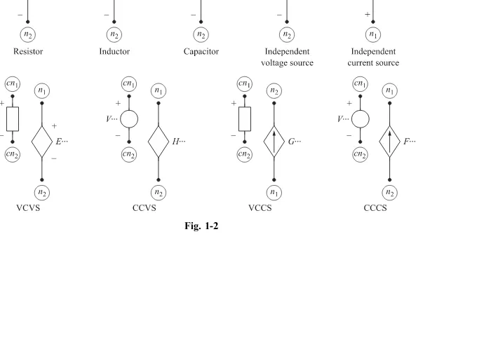
1.3. SPICE ELEMENTS
The passive and active circuit elements introduced in the previous section are all available in SPICE modeling; however, the manner of node specification and the voltage and current sense or direction are clarified for each element by Fig. 1-2. The universal ground node is assigned the number 0. Otherwise, the node numbersn1(positive node) andn2(negative node) are positive integers
i i i i i i
i L
+
_ L R
+
_ L
+
_
+
_
+
_
+
_
+
_
L L L L
+
_ V i
L C
[image:10.468.59.409.413.662.2](a) (b) (c) (d) (e) ( f ) (g) (h)
Fig. 1-1
selected to uniquely define each node in the network. The assumed direction of positive current flow is from noden1 to noden2.
The four controlled sources—voltage-controlled voltage source (VCVS), current-controlled voltage source (CCVS), voltage-controlled current source (VCCS), and current-controlled current source (CCCS)— have the associated controlling element also shown with its nodes indicated bycn1(positive) andcn2(negative). Each element is described by anelement specification statementin the SPICE netlist code. Table 1-1 presents the basic format for the element specification statement for each of the elements of Fig. 1-2. The first letter of the element name specifies the device and the remaining characters must assure a unique name.
1.4. CIRCUIT LAWS
Along with the three voltage-current relationships (1.1) to (1.3), Kirchhoff’s laws are sufficient to formulate the simultaneous equations necessary to solve for all currents and voltages of a network. (We use the termnetworkto mean any arrangement of circuit elements.)
Kirchhoff’s voltage law(KVL) states thatthe algebraic sum of all voltages around any closed loop of a circuit is zero; it is expressed mathematically as
Xn
k¼1
vk¼0 ð1:4Þ
wherenis the total number of passive- and active-element voltages around the loop under consideration.
Kirchhoff’s current law(KCL) states thatthe algebraic sum of all currents entering every node (junc-tion of elements)must be zero; that is
Xm
k¼1
ik¼0 ð1:5Þ
wheremis the total number of currents flowing into the node under consideration.
Table 1-1
Element Name Signal Type Control Source Value
Resistor R:::
Inductor L::: H
Capacitor C::: F
Voltage source V::: AC or DCa Vb
Current source I::: AC or DCa Ab
VCVS E::: ðcn1;cn2Þ V/V
CCVS H::: V::: V/A
VCCS G::: ðcn1;cn2Þ A/V
CCCS F::: V::: A/A
1.5. STEADY-STATE CIRCUITS
At some (sufficiently long) time after a circuit containing linear elements is energized, the voltages and currents become independent of initial conditions and the time variation of circuit quantities becomes identical to that of the independent sources; the circuit is then said to be operating in the
steady state. If all nondependent sources in a network are independent of time, the steady state of the network is referred to as thedc steady state. On the other hand, if the magnitude of each nondependent source can be written asKsinð!tþÞ, whereKis a constant, then the resulting steady state is known as thesinusoidal steady state, and well-known frequency-domain, or phasor, methods are applicable in its analysis. In general, electronic circuit analysis is a combination of dc and sinusoidal steady-state analysis, using the principle of superposition discussed in the next section.
1.6. NETWORK THEOREMS
Alinear network(orlinear circuit) is formed by interconnecting the terminals of independent (that is, nondependent) sources, linear controlled sources, and linear passive elements to form one or more closed paths. Thesuperposition theoremstates thatin a linear network containing multiple sources, the voltage across or current through any passive element may be found as the algebraic sum of the individual voltages or currents due to each of the independent sources acting alone, with all other independent sources deactivated.
An ideal voltage source is deactivated by replacing it with a short circuit. An ideal current source is deactivated by replacing it with an open circuit. In general, controlled sources remain active when the superposition theorem is applied.
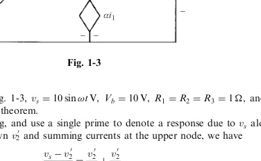
Example 1.1. Is the network of Fig. 1-3 a linear circuit?
The definition of a linear circuit is satisfied if the controlled source is a linear controlled source; that is, ifis a constant.
Example 1.2. For the circuit of Fig. 1-3,vs¼10 sin!tV, Vb¼10 V,R1¼R2¼R3¼1, and¼0. Find currenti2 by use of the superposition theorem.
We first deactivateVb by shorting, and use a single prime to denote a response due tovsalone. Using the method of node voltages with unknownv20 and summing currents at the upper node, we have
vsv
0 2 R1
¼v
0 2 R2
þv
0 2 R3
Substituting given values and solving forv20, we obtain
v20¼13vs¼103sin!t
Then, by Ohm’s law,
i20¼ v20 R2
¼10
3sin!tA R3
R2
i3
i2
L2
Ls Vb
i1
=i1
R1
_ +
_ + _
+
[image:12.468.143.331.387.503.2]_ +
Now, deactivatingvsand using a double prime to denote a response due toVbalone, we have
i300¼ Vb R3þR1kR2
R1kR2 R1R2 R1þR2
where
i300¼
10 1þ1=2¼
20 3 A so that
Then, by current division,
i200¼ R1 R1þR2
i300¼
1 2i
00 3 ¼
1 2
20 3 ¼
10 3 A Finally, by the superposition theorem,
i2¼i20þi200¼
10
3 ð1þsin!tÞA
Terminals in a network are usually considered in pairs. Aportis a terminal pair across which a voltage can be identified and such that the current into one terminal is the same as the current out of the other terminal. In Fig. 1-4, ifi1i2, then terminals 1 and 2 form a port. Moreover, as viewed to the left from terminals 1,2, networkAis a one-port network. Likewise, viewed to the right from terminals 1,2, networkBis a one-port network.
The´venin’s theoremstates thatan arbitrary linear, one-port network such as network A in Fig. 1-4(a) can be replaced at terminals 1,2 with an equivalent series-connected voltage sourceVThand impedanceZTh (¼RThþjXThÞas shown in Fig. 1-4(b). VThis the open-circuit voltage of networkAat terminals 1,2 and
ZThis the ratio of open-circuit voltage to short-circuit current of network A determined at terminals 1,2 with
network B disconnected. If network A or B contains a controlled source, its controlling variable must be in that same network. Alternatively, ZTh is the equivalent impedance looking into networkA through terminals 1,2 with all independent sources deactivated. If networkAcontains a controlled source,ZThis found as thedriving-point impedance. (See Example 1.4.)
Example 1.3. In the circuit of Fig. 1-5,VA¼4 V, IA¼2 A, R1¼2, and R2¼3. Find the The´venin
equivalent voltageVThand impedanceZThfor the network to the left of terminals 1,2.
Linear network
A
Network B
Network B
Network B
(a) (b)
2 1
2 1
(c) 2 1
i1 i2
+
_ VTh
ZTh
YN IN
Fig. 1-4
VA VB
RB
IA +
_
+
_
R1 R2 1
[image:13.468.144.319.557.667.2]2
With terminals 1,2 open-circuited, no current flows throughR2; thus, by KVL,
VTh¼V12¼VAþIAR1¼4þ ð2Þð2Þ ¼8 V
The The´venin impedanceZThis found as the equivalent impedance for the circuit to the left of terminals 1,2 with the independent sources deactivated (that is, withVAreplaced by a short circuit, andIAreplaced by an open circuit):
ZTh¼RTh¼R1þR2¼2þ3¼5
Example 1.4. In the circuit of Fig. 1-6(a),VA¼4 V,¼0:25 A=V,R1¼2, andR2¼3. Find the The´venin
equivalent voltage and impedance for the network to the left of terminals 1,2.
With terminals 1,2 open-circuited, no current flows throughR2. But the control variableVLfor the voltage-controlled dependent source is still contained in the network to the left of terminals 1,2. Application of KVL yields
VTh¼VL¼VAþVThR1
VTh¼
VA
1R1
¼ 4
1 ð0:25Þð2Þ¼8 V
so that
Since the network to the left of terminals 1,2 contains a controlled source,ZThis found as the driving-point impedanceVdp=Idp, with the network to the right of terminals 1,2 in Fig. 1-6(a) replaced by the driving-point source of Fig. 1-6(b) andVAdeactivated (short-circuited). After these changes, KCL applied at nodeagives
I1¼VdpþIdp ð1:6Þ
Application of KVL around the outer loop of this circuit (withVAstill deactivated) yields
Vdp¼IdpR2þI1R1 ð1:7Þ
Substitution of (1.6) into (1.7) allows solution forZThas
ZTh¼
Vdp
Idp
¼R1þR2
1R1
¼ 2þ3
1 ð0:25Þð2Þ¼10
Norton’s theorem states thatan arbitrary linear, one-port network such as network A in Fig. 1-4(a) can be replaced at terminals 1,2 by an equivalent parallel-connected current sourceINand admittanceYNas
shown in Fig. 1-4(c). INis the short-circuit current that flows from terminal 1 to terminal 2 due to network A, and YN is the ratio of short-circuit current to open-circuit voltage at terminals 1,2 with network B
disconnected. If network A or B contains a controlled source, its controlling variable must be in that same network. It is apparent thatYN 1=ZTh; thus, any method for determiningZTh is equally valid for findingYN.
R1 I1 Idp
Ldp R2
RL VL =VL VA
+
_
+
_ +
_ 1
2
1
2 a
(a) (b)
Example 1.5. Use SPICE methods to determine the The´venin equivalent circuit looking to the left through terminals 3,0 for the circuit of Fig. 1-7.
In SPICE independent source models, an ideal voltage source of 0 V acts as a short circuit and an ideal current source of 0 A acts as an infinite impedance or open circuit. Advantage will be taken of these two features to solve the problem.
Load resistorRLof Fig. 1-7(a) is replaced by the driving point current sourceIdpof Fig. 1-7(b). The netlist code that follows forms a SPICE description of the resulting circuit. The code is set up with parameter-assigned values forV1;I2, andIdp.
Ex1_5.CIR - Thevenin equivalent circuit .PARAM V1value=0V I2value=0A Idpvalue=1A V1 1 0 DC {V1value}
R1 1 2 1ohm
I2 0 2 DC {I2value} R2 2 0 3ohm
R3 2 3 5ohm
G3 2 3 (1,0) 0.1 ; Voltage-controlled current-source Idp 0 3 DC {Idpvalue}
.END
If bothV1andI2are deactivated by setting V1value=I2value=0, currentIdp¼1 A must flow through the The´venin equivalent impedanceZTh¼RTh so thatv3¼IdpRTh¼RTh. Execution of <Ex1_5.CIR> by a SPICE program writes the values of the node voltages for nodes 1, 2, and 3 with respect to the universal ground node 0 in a file <Ex1_5.OUT>. Poll the output file to findv3¼Vð3Þ ¼RTh¼5:75.
In order to determine VTh (open-circuit voltage between terminals 3,0), edit <Ex1_5.CIR> to set V1value=10V, I2value=2A, and Idpvalue=0A. Execute <Ex1_5.CIR> and poll the output file to find
VTh¼v3¼Vð3Þ ¼14 V.
Example 1.6. Find the Norton equivalent currentINand admittanceYNfor the circuit of Fig. 1-5 with values as given in Example 1.3.
The Norton current is found as the short-circuit current from terminal 1 to terminal 2 by superposition; it is
IN¼I12¼current due toVAþcurrent due toIA¼
VA
R1þR2
þ R1IA
R1þR2
¼ 4
2þ3þ
ð2Þð2Þ 2þ3¼1:6 A
The Norton admittance is found from the result of Example 1.3 as
YN¼ 1
ZTh
¼1
5¼0:2 S
We shall sometimes double-subscript voltages and currents to show the terminals that are of interest. Thus,V13is the voltage across terminals 1 and 3, where terminal 1 is at a higher potential than terminal 3. Similarly,I13is the current that flowsfromterminal 1toterminal 3. As an example,VLin Fig. 1-6(a) could be labeledV12(but notV21).
Note also that an active element (either independent or controlled) is restricted to its assigned, or stated, current or voltage, no matter what is involved in the rest of the circuit. Thus the controlled source in Fig. 1-6(a) will provideVLA no matter what voltage is required to do so and no matter what changes take place in other parts of the circuit.
1.7. TWO-PORT NETWORKS
The network of Fig. 1-8 is atwo-portnetwork ifI1¼I10andI2¼I20. It can be characterized by the four variablesV1;V2;I1, andI2, only two of which can be independent. If V1 andV2 are taken as independent variables and the linear network contains no independent sources, the independent and dependent variables are related by theopen-circuit impedance parameters(or, simply, thez parameters) z11;z12;z21;andz22through the equation set
V1¼z11I1þz12I2 ð1:8Þ
V2¼z21I1þz22I2 ð1:9Þ
Each of the zparameters can be evaluated by setting the proper current to zero (or, equivalently, by open-circuiting an appropriate port of the network). They are
z11¼ V1
I1
I2¼0
ð1:10Þ
z12¼ V1
I2
I1¼0
ð1:11Þ
z21¼ V2
I1
I2¼0
ð1:12Þ
z22¼ V2
I2
I1¼0
ð1:13Þ
In a similar manner, ifV1andI2are taken as the independent variables, a characterization of the two-port network via thehybrid parameters(or, simply, theh-parameters) results:
V1¼h11I1þh12V2 ð1:14Þ I2¼h21I1þh22V2 ð1:15Þ
Linear network
I1 I2
I1¢ I2¢
1 2
1¢ 2¢
+ +
V1 V2
_ _
Two of thehparameters are determined by short-circuiting port 2, while the remaining two parameters are found by open-circuiting port 1:
h11¼ V1
I1
V2¼0
ð1:16Þ
h12¼ V1 V2
I1¼0
ð1:17Þ
h21¼ I2 I1
V2¼0
ð1:18Þ
h22¼ I2 V2
I1¼0
ð1:19Þ
Example 1.7. Find thezparameters for the two-port network of Fig. 1-9. With port 2 (on the right) open-circuited,I2¼0 and the use of (1.10) gives
z11¼V1 I1
I2¼0
¼R1kðR2þR3Þ ¼ R1ðR2þR3Þ R1þR2þR3
Also, the currentIR2flowing downward throughR2 is, by current division,
IR2¼ R1 R1þR2þR3
I1
But, by Ohm’s law,
V2¼IR2R2¼ R1R2 R1þR2þR3
I1
Hence, by (1.12),
z21¼ V2
I1
I
2¼0
¼ R1R2
R1þR2þR3
Similarly, with port 1 open-circuited,I1¼0 and (1.13) leads to
z22¼ V2
I2
I1¼0
¼R2kðR1þR3Þ ¼
R2ðR1þR3Þ R1þR2þR3
The use of current division to find the current downward throughR1yields
IR1¼ R2 R1þR2þR3
I2
and Ohm’s law gives
V1¼R1IR1¼
R1R2 R1þR2þR3I2
I1 R3 I2
R1
V1 R2
[image:17.468.206.262.106.216.2]Thus, by (1.11),
z12¼ V1
I2
I1¼0
¼ R1R2
R1þR2þR3
Example 1.8. Find thehparameters for the two-port network of Fig. 1-9. With port 2 short-circuited,V2¼0 and, by (1.16),
h11¼ V1
I1
V2¼0
¼R1kR3¼ R1R3 R1þR3
By current division,
I2¼ R1 R1þR3
I1
so that, by (1.18),
h21¼ I2 I1
V2¼0
¼ R1
R1þR3
If port 1 is open-circuited, voltage division and (1.17) lead to
V1¼ R1 R1þR3
V2
h12¼ V1 V2
I1¼0
¼ R1
R1þR3
and
Finally,h22is the admittance looking into port 2, as given by (1.19):
h22¼ I2 V2
I1¼0
¼ 1
R2kðR1þR3Þ
¼R1þR2þR3
R2ðR1þR3Þ
Thezparameters and thehparameters can be numerically evaluated by SPICE methods. In electron-ics applications, thezandhparameters find application in analysis when small ac signals are impressed on circuits that exhibit limited-range linearity. Thus, in general, the test sources in the SPICE analysis should be of magnitudes comparable to the impressed signals of the anticipated application. Typically, the devices used in an electronic circuit will have one or more dc sources connected to bias or that place the device at a favorable point of operation. The input and output ports may be coupled by large capacitors that act to block the appearance of any dc voltages at the input and output ports while presenting negligible impedance to ac signals. Further, electronic circuits are usually frequency-sensitive so that any set ofzorh parameters is valid for a particular frequency. Any SPICE-based evaluation of thezandhparameters should be capable of addressing the above outlined characteristics of electronic circuits.
Example 1.9. For the frequency-sensitive two-port network of Fig. 1-10(a), use SPICE methods to determine thez
parameters suitable for use with sinusoidal excitation over a frequency range from 1 kHz to 10 kHz.
Thezparameters as given by (1.10) to (1.13), when evaluated for sinusoidal steady-state conditions, are formed as the ratios of phasor voltages and currents. Consequently, the values of thezparameters are complex numbers that can be represented in polar form aszij¼zijffij.
For determination of thezparameters, matching terminals of the two sinusoidal current sources of Fig. 1-10(b) are connected to the network under test of Fig. 1-10(a). The netlist code below models the resulting network with parameter-assigned values forII1andII5. Two separate executions of <Ex1_9.CIR> are required to determine all
Ex1_9.CIR - z-parameter evaluation .PARAM I1value=1mA I5value=0mA I1 0 1 AC {I1value}
R10 1 0 1Tohm ; Large resistor to avoid floating node Ci 1 2 100uF
RB 2 3 10kohm VB 0 3 DC 10V R1 2 4 1kohm R2 4 0 5kohm C2 4 0 0.05uF Co 5 4 100uF I5 0 5 AC {I5value}
R50 5 0 1Tohm ; Large resistor to avoid floating node .AC LIN 11 10kHz 100kHz
.PROBE .END
The values of R10 and R50 are sufficiently largeð11012Þso thatII1¼IICiandII5¼IICo. If sourceII5 is
deactivated by setting I5value=0 and I1value is assigned a small value (i.e., 1 mA), thenz11andz21are determined
by (1.10) and (1.12), respectively. <Ex1_9.CIR> is executed and the probe feature of PSpice is used to graphically display the magnitudes and phase angles ofz11andz21in Fig. 1-11(a). Similarly,II1is deactivated andII5is assigned
a small value (I1value=0, I5value=1mA) to determine the values ofz12andz22by (1.11) and (1.13), respectively.
Execution of <Ex1_9.CIR> and use of the Probe feature of PSpice results in the magnitudes and phase angles of
z12andz22as shown by Fig. 1-11(b).
Example 1.10. Use SPICE methods to determine thehparameters suitable for use with sinusoidal excitation at a frequency of 10 kHz for the frequency-sensitive two-port network of Fig. 1-10(a).
Theh parameters of (1.16) to (1.19) for sinusoidal steady-state excitation are ratios of phasor voltages and currents; thus the values are complex numbers expressible in polar form ashij¼hijffij.
Connect the sinusoidal voltage source and current source of Fig. 1-10(c) to the network of Fig. 1-10(a). The netlist code below models the resulting network with parameter-assigned values forII1 and VV5. Two separate
[image:19.468.94.362.76.491.2]Fig. 1-11
(a)
Through use of the .PRINT statement, both magnitudes and phase angles ofVV1, VV5,IICi, andIICoare written to <Ex1_10.OUT> and can be retrieved by viewing of the file.
Ex1_10.CIR - h-parameter evaluation .PARAM I1value=0mA V5value=1mV I1 0 1 AC {I1value}
R10 1 0 1Tohm ; Large resistor to avoid floating node Ci 1 2 100uF
RB 2 3 10kohm VB 0 3 DC 10V R1 2 4 1kohm R2 4 0 5kohm C2 4 0 0.05uF Co 5 4 100uF V5 5 0 AC {V5value} .AC LIN 1 10kHz 10kHz
.PRINT AC Vm(1) Vp(1) Im(Ci) Ip(Ci) ; Mag & phase of inputs .PRINT AC Vm(5) Vp(5) Im(Co) Ip(Co) ; Mag & phase of outputs .END
Set V5value=0 (deactivatesVV5) and I1value=1mA. Execute <Ex1_10.CIR> and retrieve the necessary
values ofVV1;IICi;andIICoto calculateh11andh21by use of (1.16) and (1.18).
h11¼
Vmð1Þ
ImðCiÞff ðVpð1Þ IpðCiÞÞ ffi 0:9091
0:001 ff ð0:028þ08Þ ¼909:1ff 0:028
h21¼
ImðCoÞ
ImðCiÞ ff ðIpðCoÞ IpðCiÞÞ ffi
9:08104
1103 ff ð1808þ08Þ ¼0:908ff 1808
Set V5value=1mV and I1value=0 (deactivatesII1). Execute <Exl_10.CIR> and retrieve the needed values of
V
V1;VV5;andIICoto evaluateh12andh22by use of (1.17) and (1.19).
h21¼
Vmð1Þ
Vmð5Þff ðVpð1Þ Vpð5ÞÞ ffi
9:08104
1103 ff ð0808Þ ¼0:908ff08
h22¼
ImðCoÞ
Vmð5Þ ff ðIpðCoÞ Vpð5ÞÞ ffi
3:15106
1103 ff ð84:7808Þ ¼3:1510 3ff
84:78
1.8. INSTANTANEOUS, AVERAGE, AND RMS VALUES
Theinstantaneous valueof a quantity is the value of that quantity at a specific time. Often we will be interested in the average value of a time-varying quantity. But obviously, the average value of a sinusoidal function over one period is zero. For sinusoids, then, another concept, that of the root-mean-square(orrms) value, is more useful: For any time-varying functionfðtÞwith periodT, theaveragevalue over one period is given by
F0¼ 1 T
ðt0þT
t0
fðtÞdt ð1:20Þ
and the corresponding rms value is defined as
F ¼
ffiffiffiffiffiffiffiffiffiffiffiffiffiffiffiffiffiffiffiffiffiffiffiffiffiffiffiffiffiffiffiffi 1
T ðt0þT
t0
f2ðtÞdt s
ð1:21Þ
Example 1.11. Since the average value of a sinusoidal function of time is zero, thehalf-cycleaverage value, which is nonzero, is often useful. Find the half-cycle average value of the current through a resistanceRconnected directly across a periodic (ac) voltage sourcevðtÞ ¼Vmsin!t.
By Ohm’s law,
iðtÞ ¼vðtÞ
R ¼
Vm R sin!t
and from (1.20), applied over the half cycle fromt0¼0 toT=2¼,
I0¼
1
ð
0 Vm
R sin!t dð!tÞ ¼
1
Vm
R½cos!t
!t¼0¼
2
Vm
R ð1:22Þ
Example 1.12. Consider a resistanceRconnected directly across a dc voltage sourceVdc. The power absorbed by Ris
Pdc¼ Vdc2
R ð1:23Þ
Now replaceVdcwith an ac voltage source,vðtÞ ¼Vmsin!t. Theinstantaneous poweris now given by
pðtÞ ¼v 2ðtÞ
R ¼
Vm2
R sin
2!t ð1:24Þ
Hence, theaverage powerover one period is, by (1.20),
P0¼
1 2
ð2
0 Vm2
R sin
2!t dð!tÞ ¼V 2
m
2R ð1:25Þ
Comparing (1.23) and (1.25), we see that, insofar as power dissipation is concerned, an ac source of amplitudeVmis equivalent to a dc source of magnitude
Vmffiffiffi 2
p ¼
ffiffiffiffiffiffiffiffiffiffiffiffiffiffiffiffiffiffiffiffiffiffiffiffiffiffiffi
1
T
ðT
0 v2ðtÞdt
s
V ð1:26Þ
For this reason, the rms value of a sinusoid,V¼Vm=
ffiffiffi
2
p
, is also called itseffectivevalue.
From this point on, unless an explicit statement is made to the contrary, all currents and voltages in the frequency domain (phasors) will reflect rms rather than maximum values. Thus, the time-domain voltage
vðtÞ ¼Vmcosð!tþÞwill be indicated in the frequency domain asVV¼Vj, whereV¼Vm=
ffiffiffi
2
p
.
Example 1.13. A sinusoidal source, a dc source, and a 10resistor are connected as shown by Fig. 1-12. If
vs¼10 sinð!t308ÞV andVB¼20 V, use SPICE methods to determine the average value ofiðI0Þ, the rms value of iðIÞ, and the average value of powerðP0Þsupplied toR.
The netlist code below describes the circuit. Notice that the two sources have been combined as a 10 V sinusoidal source with a 20-V dc bias. The frequency has been arbitrarily chosen as 100 Hz as the solution is independent of frequency.
Ex1_13.CIR - Avg & rms current, avg power vsVB 1 0 SIN(20V 10V 100Hz 0 0 -30deg) R 1 0 10ohm
.PROBE .TRAN 5us 10ms .END
The Probe feature of PSpice is used to display the instantaneous values ofiðtÞandpRðtÞ. The running average and running RMS features of PSpice have been implemented as appropriate. Both features give the correct full-period values at the end of each full-period of the source waveform. Figure 1-13 shows the marked values asI0¼2:0 A,
I¼2:1213 A, andP0¼45:0 W.
Solved Problems
1.1 Prove that the inductor element of Fig. 1-1(b) is a linear element by showing that (1.2) satisfies the converse of the superposition theorem.
Leti1andi2be two currents that flow through the inductors. Then by (1.2) the voltages across the inductor for these currents are, respectively,
v1¼L di1
dt and v2¼L
di2
dt ð1Þ
Now supposei¼k1i1þk2i2, wherek1 andk2are distinct arbitrary constants. Then by (1.2) and (1),
v¼L d
dtðk1i1þk2i2Þ ¼k1L di1
dt þk2L di2
dt ¼k1v1þk2v2 ð2Þ
Since (2) holds for any pair of constantsðk1;k2Þ, superposition is satisfied and the element is linear.
1.2 IfR1¼5,R2¼10,Vs¼10 V, andIs¼3 A in the circuit of Fig. 1-14, find the currentiby using the superposition theorem.
WithIsdeactivated (open-circuited), KVL and Ohm’s law give the component ofidue toVsas
i0¼ Vs R1þR2
¼ 10
5þ10¼0:667 A
WithVsdeactivated (short-circuited), current division determines the component ofidue toIs:
i00¼ R1 R1þR2Is¼
5
5þ103¼1 A
By superposition, the total current is
i¼i0þi00¼0:667þ1¼1:667 A
1.3 In Fig. 1-14, assume all circuit values as in Problem 1.2 except thatR2¼0:25i. Determine the currentiusing the method of node voltages.
By (1.1), the voltage-current relationship forR2is
vab¼R2i¼ ð0:25iÞðiÞ ¼0:25i2
so that i¼2 ffiffiffiffiffiffivab
p
(1)
Applying the method of node voltages ataand using (1), we get
vabVs
R1
þ2 ffiffiffiffiffiffivab
p
Is¼0
Rearrangement and substitution of given values lead to
vabþ10 ffiffiffiffiffiffivab
p
25¼0
Lettingx2¼vaband applying the quadratic formula, we obtain
x¼
10
ffiffiffiffiffiffiffiffiffiffiffiffiffiffiffiffiffiffiffiffiffiffiffiffiffiffiffiffiffiffi
ð10Þ24ð25Þ
q
2 ¼2:071 or 12:071
The negative root is extraneous, since the resulting value ofvabwould not satisfy KVL; thus,
vab¼ ð2:071Þ2¼4:289 V and i¼22:071¼4:142 A
R1
R2 Is
Vs +
_
a
i
b
Notice that, because the resistanceR2is a function of current, the circuit is not linear and the superposition
theorem cannot be applied.
1.4 For the circuit of Fig. 1-15, find vab if (a) k¼0 and (b) k¼0:01. Do not use network theorems to simplify the circuit prior to solution.
(a) Fork¼0, the currentican be determined immediately with Ohm’s law:
i¼ 10
500¼0:02 A
Since the output of the controlled current source flows through the parallel combination of two 100- resistors, we have
vab¼ ð100iÞð100k100Þ ¼ 1000:02ð100Þð100Þ
100þ100¼ 100 V ð1Þ (b) Withk6¼0, it is necessary to solve two simultaneous equations with unknownsiandvab. Around the
left loop, KVL yields
0:01vabþ500i¼10 ð2Þ Withiunknown, (1) becomes
vabþ5000i¼0 ð3Þ
Solving (2) and (3) simultaneously by Cramer’s rule leads to
vab¼
10 500 0 5000
0:01 500 1 5000
¼
50,000
450 ¼ 111:1 V
1.5 For the circuit of Fig. 1-15, use SPICE methods to solve for vab if (a) k¼0:001 and (b) k¼0:05.
(a) The SPICE netlist code fork¼0:001 follows:
Prb.1_5.CIR Vs 1 0 DC 10V R1 1 2 500ohm
E 2 0 (3,0) 0.001 ; Last entry is value of k F 0 3 Vs 100
R2 3 0 100ohm RL 3 0 100ohm .DC Vs 10 10 1 .PRINT DC V(3) .END
Execute <Prb1_5.CIR> and poll the output file to findvab¼Vð3Þ ¼ 101 V.
500 W
100 W 100i
10 V kLab Lab RL = 100 W
+
_
+
_
+
_ c
i
a
d 0 b
2
1 3
(b) Edit <Prb1_5.CIR> to set k¼0:05, execute the code, and poll the output file to find
vab¼Vð3Þ ¼ 200 V.
1.6 For the circuit of Fig. 1-16, findiLby the method of node voltages if (a) ¼0:9 and (b) ¼0.
(a) Withv2andvabas unknowns and summing currents at nodec, we obtain
v2vs
R1 þv2
R2
þv2vab
R3
þi¼0 ð1Þ
But i¼vsv2
R1 (2)
Substituting (2) into (1) and rearranging gives
1 R1 þ 1 R2 þ 1 R3 v2 1 R3 vab¼
1
R1
vs ð3Þ
Now, summation of currents at nodeagives
vabv2 R3
iþvab
RL
¼0 ð4Þ
Substituting (2) into (4) and rearranging yields
1
R3
R1
v2þ
1
R3
þ 1
RL
vab¼
R1
vs ð5Þ
Substitution of given values into (3) and (5) and application of Cramer’s rule finally yield
vab¼
2:1 0:1vs
0:1 0:9vs
2:1 1
0:1 1:1
¼
1:9vs
2:21¼0:8597vs
and by Ohm’s law,
iL¼
vab
RL¼
0:8597vs
10 ¼0:08597vs A
(b) With the given values (including¼0Þsubstituted into (3) and (5), Cramer’s rule is used to find
vab¼ 3 vs
1 0
3 1
1 1:1
¼
vs
2:3¼0:4348vs
i
=i
R3 = 1 9 R1 = 1 9
R2 = 1 9 RL = 10 9
TheniLis again found with Ohm’s law:
iL¼
vab
RL
¼0:4348vs
10 ¼0:04348vs A
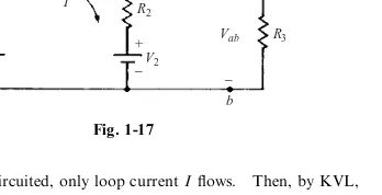
1.7 If V1¼10 V,V2¼15 V,R1¼4, andR2¼6in the circuit of Fig. 1-17, find the The´venin equivalent for the network to the left of terminalsa;b.
With terminalsa;bopen-circuited, only loop currentIflows. Then, by KVL,
V1IR1¼V2þIR2
I¼V1V2 R1þR2
¼1015
4þ6 ¼ 0:5 A so that
The The´venin equivalent voltage is then
VTh¼Vab¼V1IR1¼10 ð0:5Þð4Þ ¼12 V
Deactivating (shorting) the independent voltage sourcesV1andV2gives the The´venin impedance to the left
of terminalsa;bas
ZTh¼RTh¼R1kR2¼ R1R2 R1þR2
¼ð4Þð6Þ
4þ6¼2:4
VTh andZThare connected as in Fig. 1-4(b) to produce the The´venin equivalent circuit.
1.8 For the circuit and values of Problem 1.7, find the Norton equivalent for the network to the left of terminalsa;b.
With terminalsa;bshorted, the component of currentIabdue toV1alone is
Iab0 ¼V1 R1
¼10
4 ¼2:5 A
Similarly, the component due toV2alone is
Iab00¼
V2 R2¼
15 6 ¼2:5 A Then, by superposition,
IN¼Iab¼I
0
abþI
00
ab¼2:5þ2:5¼5 A Now, withRThas found in Problem 1.7,
YN¼ 1
RTh
¼ 1
2:4¼0:4167 A
INandYNare connected as in Fig. 1-4(c) to produce the Norton equivalent circuit.
Iab
R1 R2
V2 V1
R3
Vab I
a
b +
+
_ +
_
[image:27.468.147.321.181.270.2]_
1.9 For the circuit and values of Problems 1.7 and 1.8, find the The´venin impedance as the ratio of open-circuit voltage to short-circuit current to illustrate the equivalence of the results.
The open-circuit voltage is VTh as found in Problem 1.7, and the short-circuit current isIN from Problem 1.8. Thus,
ZTh¼
VTh
IN
¼12
5 ¼2:4
which checks with the result of Problem 1.7.
1.10 The´venin’s and Norton’s theorems are applicable to other than dc steady-state circuits. For the ‘‘frequency-domain’’ circuit of Fig. 1-18 (wheresis frequency), find (a) the The´venin equivalent and (b) the Norton equivalent of the circuit to the right of terminalsa;b.
(a) With terminalsa;b open-circuited, only loop current IðsÞflows; by KVL and Ohm’s law, with all currents and voltages understood to be functions ofs, we have
I¼ V2V1 sLþ1=sC
Now KVL gives
VTh¼Vab¼V1þsLI¼V1þ
sLðV2V1Þ sLþ1=sC ¼
V1þs2LCV2 s2LCþ1
With the independent sources deactivated, the The´venin impedance can be determined as
ZTh¼sLk 1 sC¼
sLð1=sCÞ sLþ1=sC¼
sL s2LCþ1
(b) The Norton current can be found as
IN¼VTh ZTh
¼
V1þs2LCV2 s2LCþ1
sL s2LCþ1
¼V1þs2LCV2
sL
and the Norton admittance as
YN¼ 1
ZTh¼
s2LCþ1
sL
1.11 Determine thezparameters for the two-port network of Fig. 1-19.
ForI2¼0, by Ohm’s law,
Ia¼ V1
10þ6¼
V1
16
sL
+
_
+
_ a
b IL(s)
I(s) Load
V1(s) V2(s) 1 sC
Also, at nodeb, KCL gives
I1¼0:3IaþIa¼1:3Ia¼1:3
V1
16 ð1Þ
Thus, by (1.10),
z11¼ V1
I1
I2¼0
¼16
1:3¼12:308
Further, again by Ohm’s law,
Ia¼
V2
6 ð2Þ
Substitution of (2) into (1) yields
I1¼1:3 V2
6 so that, by (1.12),
z21¼ V2
I1
I2¼0
¼ 6
1:3¼4:615
Now withI1¼0, applying KCL at nodeagives us
I2¼Iaþ0:3Ia¼1:3Ia ð3Þ
The application of KVL then leads to
V1¼V2 ð10Þð0:3IaÞ ¼6Ia3Ia¼3Ia¼3I2
1:3 so that, by (1.11),
z12¼V1 I2
I1¼0
¼ 3
1:3¼2:308
Now, substitution of (2) in (3) gives
I2¼1:3Ia¼1:3
V2
6 Hence, from (1.13),
z22¼ V2
I2
I1¼0
¼ 6
1:3¼4:615
1.12 Solve Problem 1.11 using a SPICE method similar to that of Example 1.9.
The SPICE netlist code is
b a
I1 I2
I1 I2
+
V1
_
+
V2 VB = 0
_ 10 W
6 W 0.3Ia
Ia
0
2 1
3
+ _
Prbl_12.CIR z-parameter evaluation .PARAM I1value=1mA I2value=0mA I1 0 1 AC {I1value}
F 1 0 VB 0.3 R1 1 2 10ohm
VB 2 3 0V ; Current sense R2 3 0 6ohm
I2 0 2 AC {I2value}
.DC I1 0 1mA 1mA I2 1mA 0 1mA ; Nested loop .PRINT DC V(1) I(I1) V(2) I(I2)
.END
A nested loop is used in the .DC statement to eliminate the need for two separate executions. As a consequence, data is generated forI1¼I2¼1mA andI1¼I2¼0, which is extraneous to the problem.
Execute <Prb1_12.CIR> and poll the output file to obtain data to evaluate thezparameters by use of (1.10) to (1.13).
z11¼ V1
I1
I2¼0
¼Vð1Þ
IðI1Þ
IðI2Þ¼0
¼1:23110
2
1103 ¼12:31
z12¼ V1
I2
I1¼0
¼Vð1Þ
IðI2Þ
IðI1Þ¼0
¼2:30810
3
1103 ¼2:308
z21¼ V2
I1
I2¼0
¼Vð2Þ
IðI1Þ
IðI1Þ¼0
¼4:61510
3
1103 ¼4:615
z22¼ V2
I2
I
1¼0
¼Vð2Þ
IðI2Þ
IðI1Þ¼0¼4:61510 3
1103 ¼4:615
1.13 Determine thehparameters for the two-port network of Fig. 1-19.
ForV2¼0;Ia0; thus,I1¼V1=10 and, by (1.16),
h11¼ V1
I1
V2¼0
¼10
Further,I2¼ I1and, by (1.18),
h21¼ I2 I1
V2¼0
¼ 1
Now,Ia¼V2=6. WithI1¼0, KVL yields
V1¼V210ð0:3IaÞ ¼V210ð0:3Þ V2
6 ¼ 1 2V2 and, from (1.17),
h12¼ V1 V2
I1¼0
¼0:5
Finally, applying KCL at nodeagives
I2¼Iaþ0:3Ia¼1:3
V2
6 so that, by (1.19),
h22¼ I2 V2
I1¼0
¼1:3
1.14 Use (1.8), (1.9), and (1.16) to (1.19) to find thehparameters in terms of thezparameters.
SettingV2¼0 in (1.9) gives
0¼z21I1þz22I2 or I2¼ z21 z22
I1 ð1Þ
from which we get
h21¼ I2 I1
V2¼0
¼ z21
z22
Back substitution of (1) into (1.8) and use of (1.16) give
h11¼ V1
I1
V2¼0
¼z11
z12z21 z22
Now, withI1¼0, (1.8) and (1.9) become
V1¼z12I2 and V2¼z22I2
so that, from (1.17),
h12¼ V1 V2
I
1¼0
¼z12 z22
and, from (1.19),
h22¼ I2 V2
I1¼0
¼ I2
z22I2
¼ 1
z22
1.15 The hparameters of the two-port network of Fig. 1-20 areh11¼100;h12¼0:0025;h21¼20, andh22¼1 mS. Find the voltage-gain ratio V2=V1.
By Ohm’s law,I2¼ V2=RL, so that (1.15) may be written
V2
RL
¼I2¼h21I1þh22V2
Solving forI1 and substitution into (1.14) give
V1¼h11I1þh12V2¼
ð1=RLþh22Þ h21
V2h22þh12V2
which can be solved for the voltage gain ratio:
V2 V1¼
1
h12 ðh11=h21Þð1=RLþh22Þ¼
1
0:0025 ð100=20Þð1=2000þ0:001Þ¼ 200
Two-port network
Vs V1
I1
I1
I2
I2 +
_ +
_
V2 RL = 2 kW 1 kW
+
_
1.16 Determine the The´venin equivalent voltage and impedance looking right into port 1 of the circuit of Fig. 1-20.
The The´venin voltage isV1of (1.8) with port 1 open-circuited:
VTh¼V1jI1¼0¼z12I2 ð1Þ
Now, by Ohm’s law,
V2¼ RLI2 ð2Þ
But, withI1¼0, (1.9) reduces to
V2¼z22I2 ð3Þ
Subtracting (2) from (3) leads to
ðz22þRLÞI2¼0 ð4Þ
Since, in general,z22þRL6¼0, we conclude from (4) thatI2¼0 and, from (1),VTh¼0. Substituting (2) into (1.8) and (1.9) gives
V1¼z11I1þz12I2¼z11I1 z12 RL
V2 ð5Þ
and V2¼z21I1þz22I2¼z21I1 z22
RLV2 (6)
V1is found by solving forV2and substituting the result into (5):
V1¼z11I1 z12z21 z22þRL
I1
ThenZThis calculated as the driving-point impedanceV1=I1:
ZTh¼
Vdp
Idp ¼ V1
I1 ¼z11 z12z21 z22þRL
1.17 Find the The´venin equivalent voltage and impedance looking into port 1 of the circuit of Fig. 1-20 ifRL is replaced with a current-controlled voltage source such thatV2¼I1, whereis a constant.
As in Problem 1.16,
VTh¼V1jI
1¼0¼z22I2
But ifI1¼0, (1.9) and the defining relationship for the controlled source lead to V2¼I1¼0¼z22I2
from whichI2¼0 and, hence,VTh¼0.
Now we letV1¼Vdp, so thatI1¼Idp, and we determineZThas the driving-point impedance. From (1.8), (1.9), and the defining relationship for the controlled source, we have
V1¼Vdp¼z11Idpþz12I2 ð1Þ
V2¼Idp¼z21Idpþz22I2 ð2Þ
Solving (2) forI2and substituting the result into (1) yields
Vdp¼z11Idpþz12
z21 z22
Idp
from which The´venin impedance is found to be
ZTh¼
Vdp
Idp
1.18 The periodic current waveform of Fig. 1-21 is composed of segments of a sinusoid. Find (a) the average value of the current and (b) the rms (effective) value of the current.
(a) BecauseiðtÞ ¼0 for 0 !t< , the average value of the current is, according to (1.20),
I0¼
1
ð
Imsin!t dð!tÞ ¼
Im
½cos!t!t¼¼
Im
ð1þcosÞ
(b) By (1.21) and the identity sin2x¼1
2ð1cos 2xÞ,
I2¼1
ð I
2
msin2ð!tÞdð!tÞ ¼
Im2 2
ð
ð1cos 2!tÞdð!tÞ
¼I
2
m 2 !t
1 2sin 2!t
!t¼
¼I
2
m
2 þ 1 2sin 2
I¼Im
ffiffiffiffiffiffiffiffiffiffiffiffiffiffiffiffiffiffiffiffiffiffiffiffiffiffiffiffiffiffiffiffi
þ1 2sin 2
2
s
so that
1.19 Assume that the periodic waveform of Fig. 1-22 is a current (rather than a voltage). Find (a) the average value of the current and (b) the rms value of the current.
(a) The integral in (1.20) is simply the area under thefðtÞcurve for one period. We can, then, find the average current as
I0¼1
T 4
T
2þ1
T
2
¼2:5 A
(b) Similarly, the integral in (1.21) is no more than the area under thef2ðtÞcurve. Hence,
I¼ 1
T 4
2T
2þ1
2T
2
1=2 ¼4:25 A
i, A Im
0 α p p + α 2p ωt
Fig. 1-21
T T
L, V
4
1
1 2
0 3T
2
t
1.20 Calculate the average and rms values of the currentiðtÞ ¼4þ10 sin!tA.
SinceiðtÞhas period 2, (1.20) gives
I0¼
1 2
ð2
0
ð4þ10 sin!tÞdð!tÞ ¼ 1
2½4!t10 cos!t
2 !t¼0¼4 A
This result was to be expected, since the average value of a sinusoid over one cycle is zero. Equation (1.21) and the identity sin2x¼1
2ð1cos 2xÞprovide the rms value ofiðtÞ:
I2¼ 1
2
ð2
0
ð4þ10 sin!tÞ2dð!tÞ ¼ 1
2
ð2
0
ð16þ80 sin!tþ5050 cos 2!tÞdð!tÞ
¼ 1
2 66!t80 cos!t 50
2 sin 2!t
2
!t¼0
¼66
so that I¼pffiffiffiffiffi66¼8:125 A:
1.21 Find the rms (or effective) value of a current consisting of the sum of two sinusoidally varying functions with frequencies whose ratio is an integer.
Without loss of generality, we may write
iðtÞ ¼I1cos!tþI2cosk!t
where k is an integer. Applying (1.21) and recalling that cos2x¼1
2ð1þcos 2xÞ and cosxcosy¼ 1
2½cosðxþyÞ þcosðxyÞ, we obtain
I2¼ 1
2
ð2
0
ðI1cos!tþI2cosk!tÞ2dð!tÞ
¼ 1
2
ð2
0 I12
2 ð1þcos 2!tÞ þ
I22
2 ð1þcos 2k!tÞ þI1I2½cosðkþ1Þ!tþcosðk1Þ!t
( )
dð!tÞ
Performing the indicated integration and evaluating at the limits results in
I¼ ffiffiffiffiffiffiffiffiffiffiffiffiffiffiffi I2 1 2 þ I2 2 2 r
1.22 Find the average value of the power delivered to a one-port network withpassive sign convention
(that is, the current is directed from the positive to the negative terminal) ifvðtÞ ¼Vmcos!tand iðtÞ ¼Imcosð!tþÞ.
The instantaneous power flow into the port is given by
pðtÞ ¼vðtÞiðtÞ ¼VmImcos!tcosð!tþÞ
¼1
2VmIm½cosð2!tþÞ þcos By (1.20),
P0¼
1 2
ð2
0
pðtÞdt¼Vm
4 Im
ð2
0
½cosð2!tþÞ þcosdð!tÞ
After the integration is performed and its limits evaluated, the result is
P0¼ VmIm
2 cos¼
Vmffiffiffi 2
p Imffiffiffi 2
Supplementary Problems
1.23 Prove that the capacitor element of Fig. 1-1(c) is a linear element by showing that it satisfies the converse of the superposition theorem. (Hint: See Problem 1.1.)
1.24 Use the superposition theorem to find the currentiin Fig. 1-14 ifR1¼5;R2¼10;Vs¼10 cos 2tV, and
Is¼3 cosð3tþ=4ÞA. Ans: i¼0:667 cos 2tþcosð3tþ=4ÞA
1.25 In Fig. 1-23, (a) find the The´venin equivalent voltage and impedance for the network to the left of terminalsa;b, and (b) use the The´venin equivalent circuit to determine the currentIL.
Ans: ðaÞ VTh¼V1I2R2;ZTh¼R1þR2; ðbÞ IL¼ ðV1I2R2Þ=ðR1þR2þRLÞ
1.26 In the circuit of Fig. 1-18, V1¼10 cos 2tV;V2¼20 cos 2tV;L¼1 H;C¼1 F, and the load is a 1-
resistor. (a) Determine the The´venin equivalent for the network to the right of terminalsa;b. (b) Use the The´venin equivalent to find the load currentIIL. (Hint: The results of Problem 1.10 can be used here with
s¼j2.) Ans: ðaÞ VVTh¼23:333ff08V;ZTh¼ j0:667; ðbÞ IIL¼19:4ff33:698A:
1.27 In Fig. 1-24, find the The´venin equivalent for the bridge circuit as seen through the load resistorRL.
Ans: VTh¼VbðR2R3R1R4Þ=ðR1þR2ÞðR3þR4Þ;ZTh¼R1R2=ðR1þR3Þ þR2R4=ðR2þR4Þ
1.28 Suppose the bridge circuit in Fig. 1-24 is balanced by lettingR1¼R2¼R3¼R4¼R. Find the elements of
the Norton equivalent circuit. Ans: IN¼0;YN¼1=R
1.29 Use SPICE methods to determine voltagevabfor the circuit of Fig. 1-24 ifVb¼20 V,RL¼10,R1¼1, R2¼2,R3¼3, andR4¼4. (Netlist code available at author download site.)
Ans: vab¼Vð2;3Þ ¼1:538 V
R2
I2 RL
IL R1
V1 a
b
_ +
Fig. 1-23
+
+
_ _
Vb
RL
Lab R1
R2
R3
R4
a b
0 1
2 3
1.30 For the circuit of Fig. 1-25, (a) determine the The´venin equivalent of the circuit to the left of terminalsa;b, and (b) use the The´venin equivalent to find the load currentiL.
Ans: ðaÞ VTh¼120 V;ZTh¼20; ðbÞ iL¼4 A
1.31 Apply SPICE methods to determine load currentiLfor the circuit of Fig. 1-25 if (a) the element values are as shown and (b) the VCCS has a value of 0.5vabwith all else unchanged. (Netlist code available at author
download site.) Ans: ðaÞ iL¼4 A; ðbÞ iL¼ 6 A
1.32 In the circuit of Fig. 1-26, letR1¼R2¼RC¼1and find the The´venin equivalent for the circuit to the right of terminalsa;b (a) ifvC¼0:5i1and (b) ifvC¼0:5i2.
Ans: ðaÞ VTh¼0;ZTh¼RTh¼1:75; ðbÞ VTh¼0;ZTh¼RTh¼1:667
1.33 Find the The´venin equivalent for the network to the left of terminalsa;bin Fig. 1-15 (a) ifk¼0, and (b) ifk¼0:1. Use the The´venin equivalent to verify the results of Problem 1.4.
Ans: ðaÞ VTh¼ 200 V;ZTh¼RTh¼100; ðbÞ VTh¼ 250 V;ZTh¼RTh¼125
1.34 Find the The´venin equivalent for the circuit to the left of terminalsa;bin Fig. 1-16, and use it to verify the results of Problem 1.6. Ans: VTh¼12ð1þÞvs;ZTh¼RTh¼12ð3Þ
1.35 An alternative solution for Problem 1.3 involves finding a The´venin equivalent circuit which, when con-nected across the nonlinearR2¼0:25i, allows a quadratic equation in currentito be written via KVL. Find
the elements of the The´venin circuit and the resulting current.
Ans: VTh¼25 V;ZTh¼RTh¼5;i¼4:142 A
1.36 Use (1.10) to (1.15) to find expressions for thezparameters in terms of thehparameters.
Ans: z11¼h11h12h21=h22;z12¼h12=h22;z21¼ h21=h22;z22¼1=h22
30 V +
_
+ a
_
b
Lab RL = 10 W 10 W
5 W
0.25Lab
iL
0 2 1
Fig. 1-25
Ls
LC RC
R2
R1 i1 i2
a
b +
_
+
_
1.37 For the two-port network of Fig. 1-20, (a) find the voltage-gain ratioV2=V1in terms of thezparameters,
and then (b) evaluate the ratio, using theh-parameter values given in Problem 1.15 and the results of Problem 1.36. Ans: ðaÞ z21RL=ðz11RLþz11z22z12z21Þ; ðbÞ 200
1.38 Find the current-gain ratioI2=I1for the two-port network of Fig. 1-20 in terms of thehparameters. Ans: h21=ð1þh22RLÞ
1.39 Find the current-gain ratioI2=I1for the two-port network of Fig. 1-20 in terms of thezparameters. Ans: z21=ðz22þRLÞ
1.40 Determine the The´venin equivalent voltage and impedance, in terms of thezparameters, looking right into port 1 of the two-port network of Fig. 1-20 ifRLis replaced with an independent dc voltage sourceVd, connected such thatV2¼Vd. Ans: VTh¼z12Vd=z22;ZTh¼ ðz11z22z12z21Þ=z22
1.41 Find the The´venin equivalent voltage and impedance, in terms of thehparameters, looking right into port 1 of the network of Fig. 1-20 ifRLis replaced with a voltage-controlled current source such thatI2¼ V1,
where >0 and thehparameters are understood to be positive.
Ans: VTh¼0;ZTh¼ ðh11h22h12h21Þ=ðh22þh12Þ
1.42 Determine the driving-point impedance (the input impedance with all independent sources deactivated) of the two-port network of Fig. 1-20. Ans: ðz11RLþz11z22z12z21Þ=ðz22þRLÞ
1.43 Evaluate thezparameters of the network of Fig. 1-16.
Ans: z11¼2;z12¼1;z21¼þ1;z22¼2
1.44 Find the currenti1in Fig. 1-3 if¼2;R1¼R2¼R3¼1;Vb¼10 V, andvs¼10 sin!tV.
Ans: 2 A
1.45 For a one-port network with passive sign convention (see Problem 1.22), v¼Vmcos!tV and
i¼I1þI2cosð!tþÞA. Find (a) the instantaneous power flowing to the network and (b) the average
30
Semiconductor Diodes
2.1. INTRODUCTION
Diodes are among the oldest and most widely used of electronic devices. Adiodemay be defined as a near-unidirectional conductor whose state of conductivity is determined by the polarity of its terminal voltage. The subject of this chapter is thesemiconductor diode, formed by the metallurgical junction of p-type andn-type materials. (Ap-type material is a group-IV elementdopedwith a small quantity of a group-V material;n-type material is a group-IV base element doped with a group-III material.)
2.2. THE IDEAL DIODE
The symbol for thecommon, orrectifier,diodeis shown in Fig. 2-1(a). The device has two terminals, labeledanode(p-type) andcathode(n-type), which makes understandable the choice ofdiodeas its name. When the terminal voltage is nonnegative (vD0), the diode is said to beforward-biasedor ‘‘on’’; the positive current that flows ðiD0) is calledforward current. When vD<0, the diode is said to be
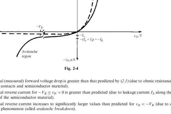
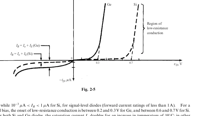
reverse-biasedor ‘‘off,’’ and the corresponding small negative current is referred to asreverse current.
The ideal diode is a perfect two-state device that exhibits zero impedance when forward-biased and infinite impedance when reverse-biased (Fig. 2-2). Note that since either current or voltage is zero at any instant, no power is dissipated by an ideal diode. In many circuit applications, diode forward voltage drops and reverse currents are small compared to other circuit variables; then, sufficiently accurate results are obtained if the actual diode is modeled as ideal.
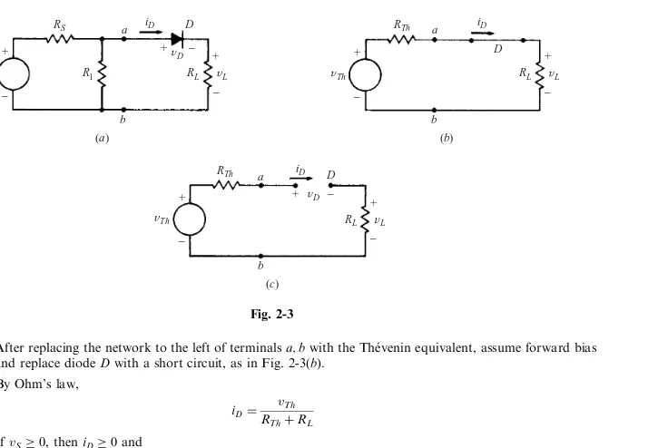
Theideal diode analysis procedureis as follows:
Step 1: Assume forward bias, and replace the ideal diode with a short circuit.
Step 2: Evaluate the diode currentiD, using any linear circuit-analysis technique.
Step 3: IfiD0, the diode is actually forward-biased, the analysis is valid, and step 4 is to be omitted. iD
Anode Cathode
+ _
D
LD
[image:38.468.42.441.50.290.2](a)
Fig. 2-1