Design of Low Power Electronic Circuits for Bio-Medical Applications
237
0
0
Full text
(2) i ABSTRACT. ABSTRACT The operational transconductance amplifier, OTA is one of the basic building blocks in many analogue circuit applications. The low power consumption is an essential parameter in modern electronic designs for many areas particularly for portable devices and biomedical applications. For biomedical applications, the lowpower low-voltage OTA-C filters operating at low-frequency ranges are desired. The low-power, low-voltage operation of electronic devices is very important for applications such as hearing aids, pacemakers, and EEG. The importance of such operation is due to the need to implant these electronic circuits inside the body of the patient for long times before re-charging or replacing the batteries as for pacemakers and future hearing aids. The small size lightweight wearable EEG systems are preferable for applications ranging from epilepsy diagnosis to brain-computer interfaces. The low power consumption is achieved by operation at very small levels of current. So, in such applications the operation in the nano-ampere current range is essential to ensure power consumption of nW or few µW. Such very small currents are obtained through the operation of MOS transistors in their sub-threshold regime. The design space in such applications is restricted by their specifications which in turn based on the nature of the application. In this work, the design and implementation of OTA-C filter topologies for two bio-medical applications are made and discussed. Those applications are represented by hearing aids and EEG applications. In hearing aids, the work focused on cochlear implant and specifically on its most important stage represented by the filter. Four OTA-C filter topologies are proposed and two of them are tested experimentally. For the filter in a hearing aid system, besides its low power operation, it is required to operate with a relatively high dynamic range of 60dB and above. The dynamic range is the operation space of the.
(3) ii ABSTRACT. filter that specified by the range of signals which can process properly. It is bounded by the maximum power signal less than its distortion overhead level to the minimum power signal more than its noise floor. The maximum signal level the filter can perform properly represents its input linear range. The challenge in CMOS OTA sub-threshold operation is the very small input linear range which makes it extremely difficult to build low-power consumed OTA-C filters with a wide dynamic range, DR. In this work, an OTA with an input linear range of ±900mV for total harmonic distortion, THD<5% is proposed using MOSFET bumping and capacitor attenuation techniques, combined for the first time. The minimum signal level the filter can distinguish from noise is still relatively small with the use of appropriate OTA architecture and using the gm/ID methodology for MOSFET sizing. So, programmable CMOS OTA-C band-pass filter topologies operating in sub-threshold region with a dynamic range of 65dB for use in bionic ears were proposed. The power consumption for the proposed filters is in nanoWatt range for their frequency range of (100-10k) Hz. Also, a 4-channel OTA-C filter bank is designed and tested. The EEG signals have small amplitudes and frequency bands ranges of µV’s and (1-40) Hz respectively. The important issue is to design filters with small noise floor with white dominant. This is achieved with the proposed OTA which is of relatively simple architecture and with operation in the deep weak-inversion region using ±1.5V supply rails. The OTA-C filter has power consumption in the pico-Watt range for δ, θ, and α signals and less than 3nW for β signals. Another topology is suggested for future work..
(4) Dedicated to my parents, aunt & sisters.
(5) iii TABLE OF CONTENTS. TABLE OF CONTENTS ACKNOWLEDGEMENTS ……………………………………………….. x. LIST OF FIGURES ………………………………………………………... xi. LIST OF TABLES …………………………………………………………. xv. PUBLICATIONS …………………………………………………………... xviii. LIST OF ABBREVIATIONS ……………………………………………... xix. LIST OF SYMBOLS ………………………………………………………. xxii. CHAPTER ONE Introduction and Review……………………………….. 1. 1.1 Introduction………………………………………………………………. 1. 1.2 Thesis contribution……………………………………………………….. 2. 1.3 Project Aims…………………………………………………………….... 2. 1.4 Organization of Thesis ………………………………………………….. 3 1.5 Hearing Aids and OTA-C Filters for their Applications ………………... 4 1.6 The Human Ear…………………………………………………………... 5. 1.7 Hearing Deficiencies……………………………………………………... 7. 1.7.1 Conductive impairment…………………………………………...... 7 1.7.2 Sensorineural impairment…………………………………………... 7. 1.8 Hearing Loss Categories…………………………………………………. 8. 1.8.1 Attenuation Loss……………………………………………………. 8.
(6) iv TABLE OF CONTENTS. 1.8.2 Compression Loss…………………………………………………... 8. 1.8.3 Perceptual Loss……………………………………………………... 9. 1.8.4 Bi-aural Loss (Bilateral hearing loss)………………………………. 9. 1.9 Hearing Aids……………………………………………………………... 9. 1.9.1 Conventional Hearing Aids………………………………………… 9 1. Completely-in-the-Canal (CIC)…………………………………... 10. 2. In-the-Canal (ITC) ……………………………………………….. 10. 3. In-the-Ear (ITE)…………………………………………………... 10. 4. Behind-the-Ear (BTE)…………………………………………….. 10. 1.9.2 Bone Anchored Hearing Aids (BAHA)…………………………...... 12. 1.9.3 Subcutaneous piezoelectric attached hearing actuator (SPAHA)...... 12 1.9.4 Middle Ear Implants (MEI)……………………………………….... 12. 1.9.5 Cochlea Implants (CI)……………………………………………… 13 1.9.6 Auditory Brainstem Implants (ABI)………………………………... 14. 1.10 The Coding Strategies of Cochlear Implant……………………………. 14 1.11 Specification of Hearing Aid Design………………………………….... 15. 1.12 The use of CMOS OTA-C Filters in Analogue Hearing Aids………….. 15. 1.13 Review of Hearing Aid Design Approaches using OTA-C Filters…….. 16 1.14 Conclusion …………………………………………………………….... 19. References……………………………………………………………………. 19. CHAPTER TWO MOSFET in Sub-threshold Regime ………………….. 25. 2.1 Introduction………………………………………………………………. 25. 2.2 MOSFET operation………………………………………………………. 25. 2.2.1 Regions of operation………………………………………………... 25. 1. Accumulation…………………………………………………… 27 2. Weak Inversion………………………………………………….. 27.
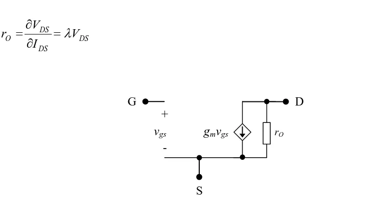
(7) v TABLE OF CONTENTS. 3. Strong Inversion………………………………………………… 28 2.2.2 MOSFET current/voltage Relations………………………………... 28. 1. Strong inversion region……………………………………......... 28 2. Small-signal model of MOSFET ……………………………….. 31. 3. Weak inversion region…………………………………………... 33. 2.3 The Test Chip…………………………………………………………….. 39. 2.3.1 Introduction………………………………………………………… 39 2.3.2 Architecture………………………………………………………… 40 2.4 Measured and simulated MOSFETs transfer characteristics……………. 41 2.4.1 Transfer Characteristics……………………………………………. 42 2.4.2 Sub-threshold swing ……………………………………………….. 44 2.5 Conclusion……………………………………………………………….. 46 References……………………………………………………………………. 47. CHAPTER THREE OTA LINEARIZATION TECHNIQUES AND THE PROPOSED OTA ……………………………………………………. 49. 3.1 Introduction………………………………………………………………. 49. 3.2 The simple OTA…………………………………………………………. 49 3.3 Techniques to increase the OTA linear range……………………………. 51. 3.3.1 Source Degeneration Technique……………………………………. 52. 3.3.2 Bumping MOSFETs Technique……………………………………. 56. 3.3.3 Capacitor Attenuation Technique…………………………………... 59. 3.4. A Review of Approaches to increase the Linear Range of OTA………... 61. 3.5 The Proposed OTA………………………………………………………. 62 3.6 MOSFET Sizing………………………………………………………….. 64. 3.6.1 The gm / ID methodology……………………………………………. 64. 3.6.2 The Inversion Coefficient Approach……………………………….. 66.
(8) vi TABLE OF CONTENTS. 3.7 Simulation Results……………………………………………………….. 67 3.7.1 OTA MOSFETs sizing utilising gm/ID methodology……………….. 67. 3.7.2 OTA transfer characteristics and Gm curve………………………… 71 3.8 Experimental Results…………………………………………………….. 76 3.9 Conclusion……………………………………………………………….. 79 References……………………………………………………………………. 80. CHAPTER FOUR Noise In Integrated Circuits ………………………… 84 4.1 Introduction………………………………………………………………. 84. 4.2 Types of noise ………………………………………………………….... 85. 4.2.1 Thermal Noise…………………………………………………….... 86. 4.2.2 Shot Noise………………………………………………………….. 88. 4.2.3 Flicker Noise……………………………………………………...... 89. 4.3 Representation of noise in circuits……………………………………… 91 4.4 Another strategy of noise representation……………………………….... 92. 4.5 Noise for MOSFET and OTA…………………………………………… 93 4.5.1 Noise in MOSFET………………………………………………….. 93. 4.5.2 Noise in the simple OTA Circuit depending on strategy of 4.3……. 94. 4.5.3 Noise in the sub-threshold simple OTA depending on strategy of 4.4…………………………………………………………………... 97. 4.5.4 Noise in Cascaded Amplifiers……………………………………... 101. 4.5.5 Noise in a system consisting of a feedback loop………………….... 102. 4.5.6 Noise in the Proposed OTA……………………………………….. 104. 4.6 Conclusion……………………………………………………………….. 106 References……………………………………………………………………. 107.
(9) vii TABLE OF CONTENTS. CHAPTER FIVE The Proposed OTA-C Filters for Cochlear Implants... 109. 5.1 Introduction………………………………………………………………. 109. 5.2 Proposed Filter Topologies………………………………………………. 109. 5.2.1 Topology 1………………………………………………………...... 109. 1. Transfer function derivation……………………………………. 110. 2. Finding the Filter poles………………………………………… 113 5.2.2 Topology 2…………………………………………………………. 114 1. Transfer function derivation…………………………………….. 115. 2. Finding the filter poles………………………………………….. 116 5.2.3 Topology 3 ……………………………………………………........ 117 1. Transfer function derivation…………………………………….. 118. 2. Finding the filter poles………………………………………….. 120 5.2.4 Topology 4……………………………………………………........ 120 1. Transfer function derivation……………………………………. 121. 2. Finding the filter poles ……………………………………….... 124. 5.3 Design Details…………………………………………………………... 125 5.3.1. Specifications……………………………………………………. 5.3.2. MOSFET Sizing………………………………………………… 125. 125. 5.4 Simulation Results………………………………………………………. 127. 5.4.1 The Frequency Response….………………………………............... 127. 1. Topologies 1 and 2…………………………………………….. 127 2. Topologies 3 and 4…………………………………………….. 129 5.4.2 Noise ………………………………………………………………. 131 1. Simulation……………………………………………………… 131 2. Noise calculations……………………………………………… 135 I.. Noise of Topology 1………………………………………. 136. II. Noise of Topology 2………………………………………. 137.
(10) viii TABLE OF CONTENTS. III. Noise of Topology 3………………………………………. 138 IV. Noise of Topology 4………………………………………. 138 5.4.3 The Filter Dynamic Range…………………………………………. 139. 5.4.4 Realisation of the Proposed Filter Topologies 3 and 4 ……………. 141 5.5 Experimental Work……………………………………………………... 142 5.5.1 Frequency Response………………………………………………... 142. 5.5.2 Noise……………………………………………………………...... 144. 5.6 Input linear range increase effect on dynamic range……………………. 147. 5.6.1 Linear range and frequency bandwidth of filter topologies. 147. 5.6.2 Dynamic range and the noise power……………………………….. 149 5.6.3 Dynamic range and the filter frequency bandwidth. 150. 5.7 The 4-Channel Filter Bank…………………………………………….... 150. 5.7.1 The Frequency Response…………………………………………. 152. 5.8 Figure of Merit………………………………………………………….. 153 5.9 Conclusion………………………………………………………………. 156. References……………………………………………………………………. 156. CHAPTER SIX PROPOSED OTA-C FILTER FOR EEG……............... 160 6.1 Introduction……......................................................................................... 160. 6.2 Design Details……………………………………………………………. 160. 6.2.1 Specifications……………………………………………………….. 160. 6.2.2 MOSFET Sizing……………………………………………………. 161 6.2.3 The operation of MOSFETs in deep weak inversion region……….. 166. 1. Mismatch and bandwidth……………………………………….. 167. 2. Noise ……………………………………………………………. 167. 6.3 The OTA-C band-pass filters for EEG…………………………………... 168 6.3.1 Design approaches……………………………………………….... 168.
(11) ix TABLE OF CONTENTS. 6.3.2 The OTA-C filter in this work…………………………………….. 169. 1. Transfer function derivation…………………………………….. 170. 2. Finding filter poles ……………………………………………... 172 6.4 Simulation Results………………………………………………………. 173. 6.4.1 The Frequency Response…………………………………………... 173. 6.4.2 Noise………………………………………………………………. 176. 6.5 Experimental Work……………………………………………………... 178 6.5.1 The Frequency Response………………………………………...... 178. 6.5.2 Noise…………………………………………………………….... 179. 6.6 Figure of Merit for the OTA-C Filter………………………………….... 182. 6.7 Conclusion………………………………………………………………. 184. References…………………………………………………………………… 185 CHAPTER SEVEN CONCLUSIONS AND FURTHER WORK ………. 187. 7.1 Conclusions………………………………………………………………. 187. 7.1.1 Cochlear Implants…………………………………………………... 187. 7.1.2 EEG Signals……………………………………………………....... 191 7.2 Further Work……………………………………………………………. 193. APPENDICIES …………………………………………………………….. 196 Appendix A Derivation of average power for correlated noise sources …….. 196. Appendix B Detailed derivations of transfer functions of the proposed Topologies……………………………………………………………………. 197. B.1 Derivation of the transfer function of Topology 1 …………………….... 197. B.2 Derivation of the transfer function of Topology 2 …………………….... 199. B.3 Derivation of the transfer function of Topology 3 …………………….... 200.
(12) x TABLE OF CONTENTS. B.4 Derivation of the transfer function of Topology 4 …………………….... 202. B.5 Obtaining the poles of the proposed Topology 4 ……………………….. 206.
(13) xi ACKNOWLEDGMENTS. ACKNOWLEDGMENTS Alhamdulillah, I hope to be able to thank almighty ALLAH for giving me the capability to say Alhamdulillah for everything.. My sincere gratitude to my Supervisor professor S. Hall for providing me with all support I needed in all years of my study. He always encourages me and gives me the important advices and notes related with all stages of my work. I’d like to thank my 2nd supervisor Dr. J. Marsland for his time, guidance and support. Also, my gratitude to my colleague Dr. Thomas Dowrick for his great help especially, in the 1st year of my study. Also I’d like to acknowledge the Iraqi ministry of Higher education and scientific research for sponsoring my study and undertaking the fabrication cost of the test chip with the department of Electrical Engineering and Electronics in the University of Liverpool which also contributes the technical support..
(14) xii LIST OF FIGURES. LIST OF FIGURES Figure 1.1 Human Ear taken from [2.1]. 5. Figure 1.2 Conventional hearing aids technologies. 11. Figure 1.3 Block diagram of a bionic ear consisting of M-channels signal processor. 13. Figure 2.1 NMOSFET, (a) Symbol. (b) Cross sectional view. 26. Figure 2.2 Ideal MOSFET small-signal model. 31. Figure 2.3 MOSFET small-signal model after adding channel modulation effect. 33. Figure 2.4 Inversion layer charge density versus distance from source to drain in the MOSFET weak inversion operation mode. 35. Figure 2.5 MOSFET small-signal model. 37. Figure 2.6 2.6mm×2.6mmm Fabricated test chip. 39. Figure 2.7 Measured and simulated transfer characteristic for MOSFETs with W=6µm, L=6µm and at VDS=0.1V. 42. Figure 2.8 Measured and simulated transfer characteristic for MOSFETs with W=30µm, L=6µm and at VDS=0.1V. 43. Figure 3.1 Simple OTA. 50. Figure 3.2 Source degradation linearization techniques for simple differential OTA; (a) Single resistor diffuser, (b) single MOSFET diffuser, (c) double MOSFETs diffusers, (d) diode connected MOSFETs. 53. Figure 3.3 Simple OTA with bumping MOSFETs technique of linearisation. 57. Figure 3.4 Simple OTA with capacitor attenuation technique. 60.
(15) xiii LIST OF FIGURES. Figure 3.5 Proposed OTA. 63. Figure 3.6 Obtaining the gm/ID versus ID/(W/L) curve; (a) NMOSFET transfer characteristics, (b) gm/ID versus VGS curve for NMOSFET, (c) PMOSFET transfer characteristics, (d) gm/ID versus VGS curve for PMOSFET, (e) The obtained the gm/ID versus ID/(W/L) curves for NMOS and PMOS transistors. 68. Figure 3.7 Normalised currents distribution in the simple OTA. 71. Figure 3.8 Normalised currents distribution in OTA with bumping MOSFETs with aspect ratio of bumping MOSFETs double that of input MOSFETs. 72. Figure 3.9 Transfer characteristics of simple, bumped, and the proposed OTAs. 73. Figure 3.10 Normalised transconductance versus differential input voltage curves for the simple, bumped, and the proposed OTAs indicating their input linear range. 74. Figure 3.11 Simulated and measured input linear range of the proposed OTA. 77. Figure 3.12 The Measured percentage variation in the input linear range of the proposed OTA. 78. Figure 4.1 Thermal noise representation of the MOSFET, (a) Thermal noise current source (b) Thermal noise voltage source. 87. Figure 4.2 Concept of flicker noise corner frequency. 90. Figure 4.3 Representation of noise by voltage and current sources. 92. Figure 4.4 Noise model of the simple OTA, (a) Taking the equivalent sources for each MOSFET (b) The overall equivalent noise model for the simple OTA. 95. Figure 4.5 Small signal noise circuit of the simple OTA. 98. Figure 4.6 Noise performance of a cascade of amplifiers,(a) A cascade of noisy amplifiers with their corresponding input-referred noise sources (b) The equivalent noise model for (a). 102.
(16) xiv LIST OF FIGURES. Figure 4.7 Block diagram of a system with a feedback loop. 103. Figure 4.8 Block diagram of a system with a feedback loop and various noise sources. 104. Figure 5.1 Proposed OTA-C filter topology1. 110. Figure 5.2 Proposed OTA-C filter topology2. 114. Figure 5.3 Proposed OTA-C filter topology3. 118. Figure 5.4 Proposed OTA-C filter topology4. 121. Figure 5.5 Simulated frequency response of the Topology 1 OTA. 128. Figure 5.6 Simulated frequency response of the Topology 2 OTA. 129. Figure 5.7 Simulated frequency response of the Topology 3 OTA. 130. Figure 5.8 Simulated frequency response of the Topology 4 OTA. 130. Figure 5.9 Simulated output noise of the Topology 1 OTA-C band-pass filter for the (100-200) Hz and (5-10) kHz frequency bands. 132. Figure 5.10 Simulated output noise of the Topology 2 OTA-C band-pass filter for the (100-200) Hz and (5-10) kHz frequency bands. 133. Figure 5.11 Simulated output noise of the Topology 3 OTA-C band-pass filter for the (100-200) Hz and (5-10) kHz frequency bands. 134. Figure 5.12 Simulated output noise of the Topology 4 OTA-C band-pass filter for the (100-200) Hz and (5-10) kHz frequency bands. 135. Figure 5.13 Simulated and measured frequency response of the proposed (Topology 1) OTA-C band-pass filter Figure 5.14 Simulated and measured frequency response of the proposed (Topology 2) OTA-C band-pass filter. 143. Figure 5.15 Measured and simulated output noise of the Topology 1 OTA-C band-pass filter for the (100-200) Hz and (5-10) kHz frequency bands. 145. 144.
(17) xv LIST OF FIGURES. Figure 5.16 Measured and simulated output noise of the Topology 2 OTA-C band-pass filter for the (100-200) Hz and (5-10) kHz frequency bands. 146. Figure 5.17 Block Diagram of the 4-Channel OTA-C Filter Bank Consisting of 4- Individual Parallel Stages of Topology 1filters. 151. Figure 5.18 Measured frequency response for the 4-channel OTA-C filter bank. 152. Figure 6.1 Measured and simulated transfer characteristic for MOSFETs with W=12µm, L=12µm and at VDS=0.1V. 162. Figure 6.2 Proposed OTA for EEG applications. 164. Figure 6.3 Proposed OTA frequency response showing the transition frequency, fT at 10pA bias current. 166. Figure 6.4 OTA-C band-pass filter for EEG applications. 170. Figure 6.5 Block diagram of the proposed OTA-C filter for EEG applications. 172. Figure 6.6 Simulated frequency response of the OTA-C filter for EEG signals. 174. Figure 6.7 Simulated frequency response of the OTA-C filter for EEG signals for nominal (straight lines) and deviation (dashed lines) cases. 175. Figure 6.8 Simulated noise of the OTA-C band-pass filter for EEG signals. 178. Figure 6.9 Measured frequency response of the OTA-C filter for EEG signals. 179. Figure 6.10 Measured noise of the OTA-C band-pass filter for EEG signals. 180.
(18) xvi LIST OF TABLES. LIST OF TABLES Table 2.1: Key device parameters for BSIM3v3.1 model in AMS process for 0.35µm CMOS C35 Technology. 41. Table 2.2: S values for figures 2.7 and 2.8 with the error. 45. Table 2.3: κ values for figures 2.7 and 2.8 figures with the error. 45. Table 2.4: Threshold voltage values for figures 2.7 and 2.8 with the error. 46. Table 3.1: The dimensions of MOSFETs of the proposed OTA. 70. Table 3.2: The simulated IB and fT ranges of the proposed OTA. 74. Table 3.3: A comparison of OTA input linear range using different linearisation techniques. 75. Table 3.4: The measured IB and fT ranges of the proposed OTA. 78. Table 4.1: Noise contribution and the noise transfer functions due to noise current sources in the simple OTA. 99. Table 5.1: The dimensions of OTA MOSFETs of the proposed topologies1 and 2. 126. Table 5.2: The dimensions of OTA MOSFETs of the proposed topologies3 and 4. 126. Table 5.3: The important simulation results related to the OTAC band-pass filter topologies 1, 2, 3, and 4 at (100200) Hz frequency band. 140. Table 5.4: The Important simulation results related to the OTAC band-pass filter topologies 1, 2, 3, and 4 at (5-10) kHz frequency band. 140. Table 5.5: The important measured results related to the OTA-C band-pass filter topologies 1 and 2 at (100-200) Hz frequency band. 146.
(19) xvii LIST OF TABLES. Table 5.6: The important measured results related to the OTA-C band-pass filter topologies 1 and 2 at (5-10) kHz frequency band. 147. Table 5.7: The figure of merit for the four proposed filter topologies in this work. 154. Table 5.8: Comparison with other weak inversion topologies presented in literature (only those with experimental results are considered except topologies 3 and 4 in this work with their simulation results). 154. Table 6.1: The sub-threshold swing and threshold voltage for figures 6.1 with the error. 163. Table 6.2: The dimensions of MOSFETs of the proposed OTA. 164. Table 6.3: The important simulated results related to the OTA-C band pass filter. 175. Table 6.4: The 1/f noise corner frequency values for EEG bands. 181. Table 6.5: The important measured results related to the OTA-C band-pass filter. 181. Table 6.6: The figure of merit for the measured EEG frequency bands. 182. Table 6.7: Comparison with other weak inversion topologies presented in literature. 183.
(20) xviii PUBLICATIONS. PUBLICATIONS 1.. S. A. Hasan, S. Hall, and J. S. Marsland, “A Proposed Sub-Threshold OTA-C for Hearing Aids,” Proceeding of 9th IEEE International NEWCAS Conference, pp. 414-417, June 2011, Bordeaux, France.. 2.. S. A. Hasan, S. Hall, and J. S. Marsland, “A Wide Linear Range OTA-C Filter for Bionic Ears,” 3rd Computer Science and Electronic Engineering Conference, CEEC’11, UK, pp.19-22, July, 2011, Essex, UK. (The best paper award)..
(21) xix LIST OF ABBREVIATIONS. LIST OF ABBREVIATIONS ABI. Auditory Brainstem Implants. AGC. Automatic Gain Control. ADC. Analogue to digital converter. AER. Address-Event Representation. AMS. Austria micro systems. B. Bulk of MOSFET. BAHA. Bone Anchored Hearing Aids. BCI. Brain-Computer Interface. BTE. Behind-the-Ear. CIC. Completely-in-the-Canal. CIs. Cochlear Implants. CLBTs. Compatible Lateral Bipolar Transistors. C-level. Comfortable level.
(22) xx LIST OF ABBREVIATIONS. CMOS. Complementary Metal Oxide Semiconductor. D. Drain of MOSFET. DSP. Digital Signal Processing. EEG. Electroencephalography. EKV. MOSFET model made by C. Enz, F. Krummenacher and E. Vitloz.. FD SOI. Fully depleted silicon on insulator wafer technology. FOM. Figure of merit. G. Gate of MOSFET. HA. Hearing Aid. ITC. In-the-Canal. ITE. In-the-Ear. KCL. Kirchhoff’s current law. M. Number of cascaded stages. MEI. Middle Ear Implants. MOSFET Metal Oxide Semiconductor Field Effect Transistor.
(23) xxi LIST OF ABBREVIATIONS. OTA-C. Operational Transconductance Amplifier- Capacitor. PFM. Pulse-Frequency Modulated. S. Source of MOSFET. SNR. Signal to Noise Ratio. SPAHA. Subcutaneous Piezoelectric Attached Hearing Actuator. T-level. Threshold level of. UV. Ultra violet. VLSI. Very Large Scale Integration. a(s). Feed forward stage in a system. e(s). Error signal in a system. f(s). Feedback stage in a system. H(s). Transfer function of the OTA-C filter.
(24) xxii ABSTRACT. LIST OF SYMBOLS a. Capacitive attenuation ratio. a-1. Number of times of increase of the input linear range due to capacitive attenuation technique. Av. Open loop voltage gain. Cdep,. Depletion region capacitance. Cgb. Gate -bulk capacitance. Cgd. Gate -drain capacitance. Cgs,. Gate -source capacitance. CIs. Cochlear Implants. CL. Total capacitance at the OTA output node “load capacitance”. COX. Gate -oxide capacitance. DR. Dynamic range. E. Electric field. f0. Centre frequency. fc. Flicker noise corner frequency. fH. High frequency. fl. Low frequency. fT. OTA transition frequency. Gm. OTA transconductance. gm. MOSFET transconductance.
(25) xxiii ABSTRACT. gmb. MOSFET bulk transconductance. gs. Summation of MOSFET’s transconductance and bulk transconductance. gsd. MOSFET source-drain conductance. IB. OTA bias current. IC. Inversion coefficient. ID. MOSFET drain current. IG. MOSFET gate current. IN. Normalised current. Iout. MOSFET output current. k. Boltzmann constant. K. Process and transistor dependent parameter. KF. Flicker noise coefficient. KFn. Flicker noise coefficient in n-channel MOSFET. KFp. Flicker noise coefficient in p-channel MOSFET. Kp. Polynomial pole coefficient in filter transfer function. Kz. Polynomial zero coefficient in filter transfer function. L. MOSFET effective length. L’. MOSFET effective length with channel length modulation. M. Number of cascaded stages. m. Ratio of the single diffussor aspect ratio to that of the input MOSFET.
(26) xxiv ABSTRACT. MB. Bumping MOSFET. MSD. Source degradation MOSFET. n. MOSFET body effect coefficient “slope factor”. N. Number of shot-noise sources. n+. High impurity n-type silicon. ne. Effective body effect coefficient. p. Pole in filter transfer function. Q. Quality factor. q. Electron charge. Q’I. Charge density of inversion layer in the weak inversion region. QB. Depletion region charge density. QFG. Floating gate residual charge. QI. Charge density of inversion layer in the strong inversion region. R. Resistor. r. Capacitor ratio in a capacitive attenuator. rO. MOSFET output resistor due to channel length modulation effect. S. Sub-threshold swing. St. Ratio of bump MOSFETs aspect ratio to that of input MOSFETs. T. Absolute temperature. THD. Total harmonic distortion. u. Velocity.
(27) xxv ABSTRACT. UT. Thermal voltage. VB. OTA bias voltage. VD. Drain voltage. Vd. OTA differential input voltage. VDS. Gate-drain voltage. VG. Gate voltage. VGB. Gate-bulk voltage. VGS. Gate-source voltage. Vin. Input voltage. Vin1. OTA non-inverting input terminal. Vin2. OTA inverting input terminal. VL. OTA Input linear range. Vout. Output voltage. VPP. Peak to peak voltage. Vrms. Volt root- mean-square- value. VS. Source voltage. VTH. Threshold voltage. W. MOSFET effective width. Δf. Frequency bandwidth. κ. Sub-threshold electrostatic coupling coefficient of the MOSFET gate and channel.
(28) xxvi ABSTRACT. кe. Effective sub-threshold electrostatic coupling coefficient between the MOSFET gate and channel. ___ 2 n Thermal. i. Thermal noise current. ___ 2 n shot. i. Shot noise current. vn, RMS. MOSFET RMS value of noise voltage. vn,eq , RMS. OTA RMS value of noise voltage. ___. v n2 1 / f . Flicker noise power. ___. v n2 Thermal. Thermal noise power. ___ 2 n , in. OTA input-referred noise power. ___ 2 n out, RMS. RMS value of output noise power. v. v. ___ 2 n in ,eq , RMS. v. RMS value of total input-referred noise power for a system consisting of many stages. ___. vn2. . MOSFET total noise power Factor affected by the MOSFET operation regime which equals to ½ and 2/3 for sub-threshold and above threshold respectively. λ. Channel length modulation parameter. µn. Average mobility of electrons. µO. Low-field mobility. µp. Average mobility of holes. ψs. Surface potential.
(29) 1 CHAPTER ONE. Introduction and Review. CHAPTER ONE Introduction and Review 1.1 Introduction Analogue integrated OTA-C filters are the most important building stages in wearable and implantable medical devices such as cochlear implants, CI and Electroencephalography, EEG systems. Such devices are used for many purposes such as diagnosing medical problems, restoring lost body functions, and brain–computer interface (BCI) systems [1.1]. Due to the nature of physiological signals and the corresponding application scenarios, the filters designed for such low frequency applications should meet stringent specifications. The most important specifications are represented by efficient power consumption, low voltage operation, low input-referred noise, high performance and flexibility.. The objective of designing circuits with low power consumption in the range of micro watts is to increase the battery life-time. This means that the systems can operate for a long time in terms of years instead of days or weeks before the need to recharge or replace their batteries. The low voltage operation allows the use of small size batteries which is reflected in a decrease of the entire size of the system. Also, many other specifications like price should be taken in account, hence, the choice of whether to use analogue or digital configurations for the filter and the other stages of such systems. Furthermore the choice of DSP strategies for the entire system depends on the trade-offs in satisfying the required specifications. Therefore, adopting hybrid mixed-signal implementation should give the best compromise for these applications. Therefore, a. LOW POWER ELECTRONIC CIRCUITS FOR BIOMEDICAL APPLICATIONS. Saad A. Hasan.
(30) 2 CHAPTER ONE. Introduction and Review. system consisting of analogue and digital parts is feasible since in CMOS technology this can be accomplished on the same chip. A filter has a dynamic range of operation limited by two constraints. The first one is the upper limit above which the output is distorted. This limit is represented by the filter input linear range. The lower limit is the input-referred noise floor. In this work, both limits of the dynamic range of the proposed filters are discussed in detail. Besides, the upper limit is increased, especially for the filters which are proposed for hearing aids application. This work provides the trade-offs in satisfying the specifications for cochlear implants and EEG applications.. 1.2 Thesis Contribution In this work, an OTA with a large input linear range of ±900 mV is presented. This is accomplished by combining MOSFET bumping and capacitor attenuation techniques together, for the first time. In this approach, the proposed OTA has a simple structure and relatively low noise. The proposed OTA is used to construct four, 2nd order OTA-C band-pass filter topologies suitable for hearing aids applications. Two of those filters are tested experimentally. A parallel 4-channel OTA-C filter bank for hearing aids applications is also proposed and experimentally tested. Finally, a 4th order OTA-C band-pass filter suitable for EEG applications is proposed, built, and tested experimentally.. 1.3 Project Aim The target of this research is to develop low power electronic circuits that can be used as a frequency extraction stage in modern biomedical applications such as hearing aids and EEG systems. Hearing aids are used to overcome hearing deficiencies that. LOW POWER ELECTRONIC CIRCUITS FOR BIOMEDICAL APPLICATIONS. Saad A. Hasan.
(31) 3 CHAPTER ONE. Introduction and Review. arise from simple problems related to outer or middle ear to severe problems due to damage in the inner ear.. Electroencephalography is a tool to record signals that represent the brain electrical activity which are measured by electrodes placed on the scalp. The EEG signals lie within four different frequency bands namely δ, θ, α, and β, characterised by their low voltage amplitudes and frequency. Those signals reflect different human activities and are very important in clinical tests for diagnosis ranging from epileptic fits to brain death and other brain disorders. Recently EEG signals are also used in computer- brain interface systems, CBI which represents a direct communication pathway between the brain and an external device [1.2]. This application is aimed to augment, assist or repair human cognitive or sensory-motor functions. An example of this is the enabling of signals from the brain to control some external activity to help a person suffering from paralysis to write a book, control a prosthetic limb or a motorised wheelchair. The CMOS OTA-C filters operate with very small power that on the one hand enables utilizing batteries as long as possible. Moreover, this opens up the scope to innovate very small size electronic circuits to be completely implanted inside the patient body for longer times than those currently available. The designs are inspired by the operation of the biological human auditory system. Also, earlier hearing technologies and auditory models are studied to identify their properties to allow comparison with the results obtained in this work. EEG signals are also studied. The acquired knowledge in such biological systems is exploited in proposing an OTA-C filter suitable for EEG applications.. 1.4 Organisation of Thesis The thesis is divided into seven chapters. The 1st chapter gives a brief introduction about the filters used in biomedical applications. This is followed by a summary of the human auditory system, hearing deficiencies, hearing aid technologies, and a review of. LOW POWER ELECTRONIC CIRCUITS FOR BIOMEDICAL APPLICATIONS. Saad A. Hasan.
(32) 4 CHAPTER ONE. Introduction and Review. previous work in this context represented by proposed cochlea implant technology and OTA-C filters. The 2nd chapter presents MOSFET regions of operation with a focus on the sub-threshold regime. The range of operation of the OTA-C is determined by its dynamic range. Because of the great importance on this factor on the filter performance, its constraints are discussed in details. These constraints are represented by its upper and lower limits. The upper limit is the input linear range of the filter i.e. the maximum allowable input before distortion while the lower limit represents its input-referred noise floor. Discussing these two limits is done by allocating the 3rd and 4th chapters for this purpose. The 3rd chapter describes some of most commonly techniques used to increase the input linear range “increasing the upper limit of the dynamic range”. The proposed OTA is introduced in the same chapter and compared with some other designs. This OTA is utilised to construct the OTA-C filters suited for cochlear implants. Since the lower limit of the filter dynamic range is the input-referred noise floor therefore the 4th chapter explains in detail the noise in integrated circuits, their types and representations. The 5th chapter presents the proposed OTA-C filter topologies and the 4-channel filter bank suitable for cochlear implants. Also, the derivations of filters transfer functions are detailed and their frequency response and noise curves obtained experimentally are compared with other published work. The 6th chapter describes the realisation of the proposed OTA and OTA-C filter for EEG applications and a comparison is made with prior work made by other researchers. Conclusions are drawn in the 7th chapter, together with suggestions for further work.. 1.5 Hearing Aids and OTA-C Filters for their Applications The main parts of the human ear and their anatomy are now briefly presented and their functions described. Hearing deficiencies are then explained and the hearing loss categories are classified according to the physiological impairments. The hearing aids used according to hearing losses are summarised. The human auditory system has unique features, so the necessary specifications for the electronic circuits used for LOW POWER ELECTRONIC CIRCUITS FOR BIOMEDICAL APPLICATIONS. Saad A. Hasan.
(33) 5 CHAPTER ONE. Introduction and Review. hearing aids applications are mentioned. In the introduction the use of CMOS OTA-C filters in analogue hearing aids is later presented with a critical review of proposed approaches in the field of cochlea implant design. A number of CMOS OTA-C filter designs of are reviewed.. 1.6 The Human Ear A brief description of the anatomy of the outer, middle and inner ear [1.3] is now presented. The human ear is a system that operates like a transducer, translating the acoustic energy into electrical nerve energy, which then passes to the brain. Figure 1.1 shows the human ear with its three parts, namely; the outer, middle, and inner ear.. Figure 1.1 Human Ear taken from [1.3]. The outer ear consists of the pinna, the concha, and the ear canal. It provides for the efficient transmission of the acoustic wave from the environment to the eardrum. Also, as a result of its depth and shape, it protects both eardrum and the middle ear from. LOW POWER ELECTRONIC CIRCUITS FOR BIOMEDICAL APPLICATIONS. Saad A. Hasan.
(34) 6 CHAPTER ONE. Introduction and Review. the external environment and direct injury. It performs some other actions represented by increasing the pressure of the acoustic wave for some frequencies causing resonance in its cavity. Finally, the outer ear can be thought of as a sound directional amplifier aiding an individual in recognizing and localizing sounds.. The middle ear is a cavity within the skull bone, filled with air. It is represented by the eardrum in addition to the chain of three small bones: malleus, incus, and stirrup, known as the ossicular chain. It is suspended in this cavity by small muscles. The malleus is promptly attached to the eardrum, while the incus and the stirrup are attached to the malleus and oval window respectively. The acoustic wave that reaches the eardrum is transmitted to the oval window as a mechanical vibration. It is worth noting that the ossicular chain, oval window and eardrum provide acoustic impedance matching. This leads to more efficient transfer of the mechanical vibration to the inner ear. The inner ear is a fluid-filled bony structure embedded deeply in the temporal bone of the skull. It consists of the cochlea and auditory nerve. Generally, the inner ear performs the conversion of the mechanical vibration represented by the pressure wave coming from the oval window into electrical nerve signals or “spikes” to be communicated with the central nervous system and hence to the brain. The sound pressure wave propagates down the fluid and membrane structure of the cochlea by their combined movement. Since the fluid is incompressible and according to the fluid mass conservation, the round window moves in opposition to the stirrup, as obtained experimentally [1.4].. The basilar membrane is narrow and stiff and is situated at the cochlea basal end. Hence, the membrane-displacement waves propagate quickly with a long wavelength. As the wave travels down the cochlea, the membrane stiffness decreases, the waves become slower, shorter, and increase in amplitude. At some point, known as the best place for the given input frequency, the membrane vibrates with maximum. LOW POWER ELECTRONIC CIRCUITS FOR BIOMEDICAL APPLICATIONS. Saad A. Hasan.
(35) 7 CHAPTER ONE. Introduction and Review. amplitude. Beyond that position, the basilar membrane becomes too flexible and highly damped to support wave propagation at that frequency, and dissipates rapidly, the wave energy beyond it. It is worth noting that the maximum displacement position of the basilar membrane is observed to vary approximately logarithmically with the frequency of the input [1.5].. From the electrical engineering point of view, the cochlea can be considered as a frequency analyzer and feature exactor for the acoustic input. Also, the outer hair cells within the cochlea have active characteristics in controlling the gain of certain frequency bands [1.6].. 1.7 Hearing Deficiencies Hearing deficiencies can be classified into the following main reasons. 1.7.1 Conductive impairment. This impairment is in the outer or middle ear, making them unable to pass acoustic energy properly to the inner ear. In this case the acoustic wave suffers from attenuation. This type of impairment can be overcome by using a simple hearing aid. This hearing impairment may be due to a disease in the outer ear or damage to the ear drum.. 1.7.2 Sensorineural impairment. This impairment occurs in the inner ear. It may be a result of exposure to high volume levels or bacterial infection which leads to damage of the inner ear, or due to aging of the basilar membrane which causes changes in its features by make it stiffer and less elastic. In this case the acoustic wave suffers attenuation and distortion. A more LOW POWER ELECTRONIC CIRCUITS FOR BIOMEDICAL APPLICATIONS. Saad A. Hasan.
(36) 8 CHAPTER ONE. Introduction and Review. complicated hearing aid is needed for such types of impairment compared to that related with outer or middle ear defects.. 1.8 Hearing Loss Categories As a result of the two above sources of physiological impairments, the following four categories of hearing loss appear.. 1.8.1 Attenuation Loss. This type of loss takes place due to conductive or sensorinueral impairments. It appears as attenuation in amplitude of a range of frequencies. Its effect on hearing is to perceive one part of sound or speech to be quieter than the other. This loss can be measured by the use of an audiogram [1.7]. One of the techniques is linear amplification that uses a constant gain to compensate for such attenuation. There are other techniques which depend on non-linear amplification [1.8]. Some other techniques are used to explain the nature of hearing impairments and suggest or eliminate compensatory signal-processing schemes for them [1.9].. 1.8.2 Compression Loss. In this case, due to sensorinueral impairment, the dynamic range of sounds is compressed resulting in the inability to recognize sound levels. This is because the threshold level (T-level) becomes higher or the maximum level of comfortable listening of loud sounds (C-level) is changed. This loss can be measured using the audiogram by setting the categorical loudness scaling [1.7]. An appropriate signal processing scheme for compensation in accordance to the loss level can be used. This is done by reducing the dynamic range to that of the patient.. LOW POWER ELECTRONIC CIRCUITS FOR BIOMEDICAL APPLICATIONS. Saad A. Hasan.
(37) 9 CHAPTER ONE. Introduction and Review. 1.8.3 Perceptual Loss. This type of loss also belongs to sensorinueral impairment, whereby due to background noise, the speech intelligibility is reduced. When the signal to noise ratio, SNR is high, it reduces the noise ability in masking the sound fundamental elements. For low SNR levels, the noise effect becomes obvious. In this case, the hearingimpaired can not distinguish speech. The adaptive signal processing scheme for compensation of such loss is used [1.10].. 1.8.4 Bi-aural Loss (Bilateral hearing loss) This type of loss is a result of sensorinueral impairment. Because of impairment in analysing the information from both ears, the patient is unable to recognize between speech and noise as well as failure in localising sound sources. An adaptive signal processing scheme with two inputs from different sound sources can reduce the problem [1.11].. 1.9 Hearing Aids A hearing aid is an electro-acoustic, body-worn apparatus which typically fits in or behind the wearer's ear, and is designed to amplify and modulate sounds for the wearer. There are following basic types of hearing-aid technologies. 1.9.1 Conventional Hearing Aids. These have a microphone input followed by a processing stage to change acoustic characteristics as required. The processed signal goes to the ear drum and auditory system. This type of hearing aid includes four styles as explained below. LOW POWER ELECTRONIC CIRCUITS FOR BIOMEDICAL APPLICATIONS. Saad A. Hasan.
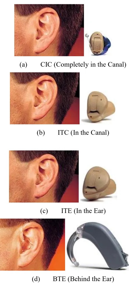
(38) 10 CHAPTER ONE. Introduction and Review. 1. Completely-in-the-Canal (CIC). This style is shown in Figure 1.2 (a). It is the smallest type of hearing aid made and is almost invisible in the ear. All its components are housed in a small case that fits deeply inside the ear canal. These hearing aids are restricted to persons with ear canals large enough to accommodate the insertion depth of the instrument into the ear and it is suitable for mild to moderate hearing losses. Also it is most difficult to place and adjust.. 2. In-the-Canal (ITC). This is slightly larger than the CIC as shown in Figure 1.2 (b), but is still unobtrusive. It fits down in the canal of the ear and is relatively unnoticeable. It is easier to use compared to the CIC type despite that it has a slightly larger battery than the CIC. It is suitable for use with mild to moderate hearing impairment.. 3. In-the-Ear (ITE). This is a larger device which fills the "bowl" of the ear as in Figure 1.2 (c). Due to its larger size, it can accommodate biggeraudio amplifiers and more features such as a telephone switch. It is easier to use than CIC or ITC models. These hearing aids can be used for a wider range of hearing losses. 4. Behind-the-Ear (BTE). This is presented in Figure 1.2 (d) which shows circuitry and microphone fitting behind the ear. It meets a wide range of hearing needs, including severe hearing impairments. Due to its robust design, this style is especially recommended for children. It aids can provide more amplification than smaller devices due to the large amplifier and battery.. LOW POWER ELECTRONIC CIRCUITS FOR BIOMEDICAL APPLICATIONS. Saad A. Hasan.
(39) 11 CHAPTER ONE. Introduction and Review. (a). CIC (Completely in the Canal). (b). (c). (d). ITC (In the Canal). ITE (In the Ear). BTE (Behind the Ear). Figure 1.2 Conventional hearing aids technologies. LOW POWER ELECTRONIC CIRCUITS FOR BIOMEDICAL APPLICATIONS. Saad A. Hasan.
(40) 12 CHAPTER ONE. Introduction and Review. 1.9.2 Bone Anchored Hearing Aids (BAHA). The BAHA soft band and implanted system is more beneficial over traditional bone-conduction hearing aids The BAHA is an auditory prosthetic which can be surgically implanted. It uses the skull as a pathway for sound to travel to the inner ear. For people with severe conductive losses, the BAHA is used to bypass the external auditory canal and middle ear, and send the acoustic vibrations to the cochlea [1.12]. For people with unilateral hearing loss, the BAHA uses the skull to conduct the sound from the deaf side to the side with the functioning cochlea.. 1.9.3 Subcutaneous piezoelectric attached hearing actuator (SPAHA). This is a more advanced hearing aid proposed for compensation of conduction loss [1.13]. It is based on a piezoelectric bending actuator. The device lies flat against the skull which would allow it to form the basis of a subcutaneous bone-anchored hearing aid. The bone-bending excitation is obtained through a local bending moment rather than the application of a point force as in the BAHA. Cochlear velocity measurements are created by the actuator, leading to a high efficiency, making it a possible future candidate for electromagnetic bone-vibration actuators [1.13].. 1.9.4 Middle Ear Implants (MEI). The MEI implant is directly fixed to one of the ossicles in the middle ear, leaving the ear canal free. This is preferable especially for patients more sensitive to foreign objects inside their ear canals. Another advantage is the ability to cancel the feedback loop effect which is apparent in conventional hearing aids [1.14].. LOW POWER ELECTRONIC CIRCUITS FOR BIOMEDICAL APPLICATIONS. Saad A. Hasan.
(41) 13 CHAPTER ONE. Introduction and Review. 1.9.5 Cochlea Implants (CI). This consists of two basic units, the electrode array and the signal processing unit. The array of electrodes is surgically implanted either inside or against the outside of the cochlea to directly mimic the auditory nerve. The signal processing units consist of many stages generally represented by microphone, the preamplifier and automatic gain control, band-pass filter bank, envelope detector, compressor, and the modulator. Figure 1.3 shows the block diagram of the cochlear implant “bionic ear”. The acoustic input is converted to electrical signals by the microphone, and then processed by the pre-amplifier and automatic gain control stage. The band-pass filter divides the signal into different frequency bands, and then the envelope “peak” of each band is detected by the envelope detector. The dynamic range of each band is compressed to fit to the patient and then sent to the modulator. The modulated signal bands are then sent to the electrode array which in turn, provides stimulation of the patient’s neurons [1.15], [1.16]. The number of patients who use the cochlear implants is 200000 around world [1.17].. Microphone. Band-Pass Filter (1). Envelope Detector. Non-Linear Compression. Modulation. Electrode 1. Band-Pass Filter (M). Envelope Detector. Non-Linear Compression. Modulation. Electrode M. Pre-Emphasis and AGC. Figure 1.3 Block diagram of a bionic ear consisting of M-channels signal processor. The challenge related to the CI is the relatively high power consumption, which needs to be reduced from milli-volts to micro-volts [1.18] in order to increase the. LOW POWER ELECTRONIC CIRCUITS FOR BIOMEDICAL APPLICATIONS. Saad A. Hasan.
(42) 14 CHAPTER ONE. Introduction and Review. battery life time. Many approaches have been proposed to cope with this difficulty and are described in section 2.8. The aim is to satisfy the necessary specifications, outlined in section 2.6, to meet the features of the biological cochlea.. 1.9.6 Auditory Brainstem Implants (ABI). This is a surgically implanted device to provide a sense of sound to profoundly deaf individuals. In this case, the patients are suffering from illness or injury damaging their cochleas or auditory nerves. So, the stimulation of the brain stem of the recipient is required. This is obtained with the suitable technology and the brain surgery for device implantation. Much effort is being spent in this context to develop and use the auditory brainstem implants to stimulate nerves by electrodes and transfer directly the information to auditory brain stem [1.19].. 1.10 The Coding Strategies of Cochlear Implant The essential objective of using the signal processor is to decompose the input signal into its frequency components. This is accomplished by dividing the input signal into different frequency bands then sending the filtered signals to the appropriate electrodes. The coding strategy can allow identification of the approaches used to alter the acoustic input features to satisfy convenient nerve stimulation within the cochlea. Developing coding strategies with appropriate noise reduction algorithms leads to the specification of advanced cochlear implants. This enables the hearing-impaired to get the best understanding of the acoustic signal on the one hand, whilst increasing the discrimination ability between the signal and noise for better patients communication in noisy environments, on the other hand[1.15].. LOW POWER ELECTRONIC CIRCUITS FOR BIOMEDICAL APPLICATIONS. Saad A. Hasan.
(43) 15 CHAPTER ONE. Introduction and Review. There are many coding strategies. Some of those are Maximum Spectral Peak Extraction [1.20], Compressed Analogue [1.21], Continuous Interleaved Sampling [1.22], and Spectral Maxima Sound Processor [1.23].. 1.11 Specification of Hearing Aid Design The hearing aids have some specifications that are always considered by designers. This is to mimic some unique aspects offered by the biological auditory system and to make it acceptable for most users. The HA design should consume a minimum possible power to increase the battery life time. This is very important especially for fully implanted future cochlear aids. They should operate with small voltage rails to use small batteries which mean small size devices. The operational reliability using appropriate signal processors and flexibility by adopting or proposing good designs are important. Finally, the hearing aid devices should satisfy all or most of the above requirements with a minimal possible cost.. 1.12 The use of CMOS OTA-C Filters in Analogue Hearing Aids In analogue circuits, filters can be considered as basic building blocks [1.24]. Filters can be utilised in many audio applications such as speech recognition, processing for cochlear implants, and other applications. OTA-C filters are the most power efficient choices for low power, low-voltage, and low frequency applications. They use the transconductance of transistors, usually operating in sub-threshold and use buffering directly. For micro-power audio applications, generally either OTA-C or log domain filters are used. They are preferred over other approaches such as MOSFET-C and switch capacitor filters. The MOSFET-C filters have additional requirements represented by an amplifier with a high gain and higher bandwidth than that of the filter itself. The switch capacitor filters suffer from sampling errors and problems which may. LOW POWER ELECTRONIC CIRCUITS FOR BIOMEDICAL APPLICATIONS. Saad A. Hasan.
(44) 16 CHAPTER ONE. Introduction and Review. appear due to clock feed-through. In spite of the successful use of log domain filters in micropower applications, they have some disadvantages. One of these is the noise signal which is affected by the input signal level. Also, the log domain filters performance is highly sensitive to device mismatch. Such mismatch causes distortion due to the non-linear nature of those filters, such that their performance needs to be assessed using specific tests [1.25]. OTA-C filters on the other hand, offer the low power and wide tuneable frequency range required in hearing aids applications. One major limitation of sub-threshold OTA-C filters is represented by their narrow input linear range. From the above points, it can be concluded that the OTA-C filters can represent the best choice for such applications when their linear range is increased properly.. 1.13 Review of Hearing Aid Design Approaches using OTA-C Filters The biological cochlea is a good example of a complete system. It can sense 0.5nm of eardrum motion at its best frequency. Its input dynamic range spans 12 orders of magnitude in sound intensity that is 120 dB. It operates over a frequency range of about 3 decades with a power dissipation of merely a few tens of microwatts [1.26] Hearing aids and particularly cochlear implants play an important role to help people suffering from severe hearing problems. It is now possible to restore partial hearing for people with such deficiencies. Efforts of many scientists and researchers from various disciplines results in many approaches in the field of cochlea implant design. A review of some approaches in that context based on CMOS OTA-C filters which have been proposed and successfully tested, is summarized below. Lyon et al in 1988 [1.27] produced the widely known, Lyon and Mead silicon cochlea model. The analogue electronic cochlea has been built in MOSIS CMOS VLSI technology using micropower techniques with sub-threshold operation. The key point of the model and circuit is a cascade of 480 stages of 2nd order filters which are simple, LOW POWER ELECTRONIC CIRCUITS FOR BIOMEDICAL APPLICATIONS. Saad A. Hasan.
Figure
![Figure 1.1 Human Ear taken from [1.3]](https://thumb-us.123doks.com/thumbv2/123dok_us/8058997.225491/33.595.170.467.356.558/figure-human-ear-taken-from.webp)


+7


Related documents
Free fluid content, thickening time and expansion capability of the high-resistant cements are adjusted by adding polyvinyl alcohol, lignosulfonate and MgO,
Volatility Model Choice for Sub-Saharan Frontier Equity Markets - A Markov Regime Switching Bayesian Approach.. Carl
How does the free energy behave close to the critical curve? How large are the excursions of the path away from the horizontal?.
• Identify trends and opportunities for optimization based on your real-world outcomes.. • Customize your personal
[r]
18 This should be demonstrated using an auditing tool, The University of Reading Template for Career Management Skills, which is designed to identify and record where a
“I want to refer my patients to a fitness professional, but how do I know who to trust?” This is a common question from health care providers who recognize that exercise is one
Any graduate who can satisfy the provisions of A31(1), may qualify as a social worker by passing the undermentioned study units for non- degree purposes (NDP) provided that
