EtherLink Plus Adapter Technical Reference
Manual
A Member of the EtherLink Product Family
Copyright © 3Com Corporation, 1988. All rights reserved. 3165 Kifer Road
Santa Clara, California 95052-8145 Printed in the U.S.A.
Copyright Statement
No part of this manual may be reproduced in any form or by any means or used to make any derivative (such as translation, transfonnation or adaption) without pennission from 3Com Corporation, by the United States Copyright Act of 1976, as amended.
Disclaimer
3Com makes no warranty of any kind with regard to this material, including, but not limited to, the implied warranties of merchantability and fitness for a particular purpose. 3Com shall not be liable for errors contained herein or for incidental or consequential damages in connection with the furnishing, performance, or use of this .lnaterial.
Contents
Preface v
Chapter 1: Introduction
About this Document 1-1 Overview 1-2
Programming 1-2
Chapter 2: Hardware Reference
Introduction 2-1 Address Maps 2-2
Adapter I/O Map: 80186 On-board I/O Ports 2-2 Adapter Memory Map 2-3
Host I/O Map: Adapter's external I/O ports 2-3 80186 Microprocessor 2-3
82586 Ethernet Coprocessor 2-4 Network Interface 2-4
82586 Serial Interface 2-4 8023 Manchester Converter 2-5 Transceiver 2-5
Adapter Firmware ROM 2-5 Adapter RAM 2-6
Host-Adapter Interface 2-7 Command Register 2-8 Data Register 2-8
Data Register Configuration 2-9 DMA Transfer 2-9
Status Flags 2-10
Adapter (80186) Interrupts 2-10 Internal Interrupts 2-10 Externallnterrupts 2-11 Host Interrupts 2-11 Resetting the Adapter 2-12 Station Address 2-13 LED Indicators 2-13 Host ROM 2-13
Chapter 3: Hardware Interface
Introduction 3-1
Command Register 3-1 Data Register 3-2
Host Control Register 3-2
Host Status Register 3-3 Host AUX DMA Register 3-4 Adapter Control Register 3-5 Adapter Status Register 3-6
Chapter 4: Command Interface
Introduction 4-1
Primary Command Block Structure 4-1 Status Flag Usage for PCB Transfer 4-3 Host to Adapter Request 4-4
Adapter to Host Request or Response 4-4 PCB Commands 4-5
Host to EtherLink Plus Adapter PCB Formats 4-5 EtherLink Plus Adapter to Host PCB Formats 4-9 System ROM Utilities 4-13
Host I/O Support: INT 80H 4-13 Network I/O Support: INT 81 H 4-16 Configuration Status: INT 82H 4-17 Timer Support: INT 83H 4-19
Download Program Support: INT 84H 4-20 PCB Command Processor: INT 85H 4-20 Packet Processor Vector: INT 86H 4-21 Idle Vector: INT 87H 4-22
PCB Enqueue Vector: INT aaH 4-22
Chapter 5: Programming
PCBs 5-1 Interrupts 5-2
Data Transfer and DMA 5-2 ROM Utilities 5-3
Data Structure 5-3 .
Appendix A: 80186 Peripheral Control Block Programming
Appendix B: 82586 Parameter Example
Appendix C: Diagnostics
Diagnostic Command Format C-2 Requirements for Testing C-3
Running the 3C505.EXE Program C-3
3C501 / 3C505 Diagnose Program Differences C-4
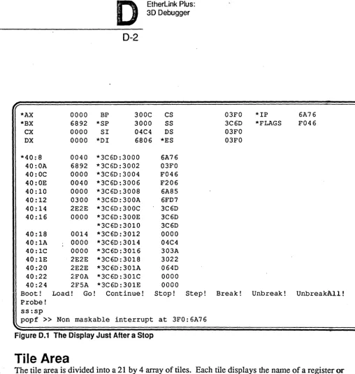
Appendix D: 3D Debugger
Tile Area D-2 Menu Bar 0-2 Typein Area 0-3
Using the Mouse to Control the Display 0-3 Function Keys D-4
Appendix E: Software Diskette
Appendix
F:
Revision 2.0 ROM
Configure Adapter Memory F-1 Timeout Values F-1
Timestamp and Timer Resolution F-2 DMA Downloading Programs F-2
Zero Offset Problem for Downloaded Programs F-2 Receive/Return Packet functions F-2
PCB Formats F-2
Interrupt Vector Services F-3 TEST Jumper Usage F-3
Configure 82586 Receive Mode F-3 Receive Packet PCB Timeout F-4 Loopback Mode F-4
Appendix
G:
Revision 3.0 ROM
Adapter Selftest Command G-1 Transmit Packet Command G-1
Get Adapter Information Command G-1 Packet Processor G-1
Adapter LEOs G-1
Power On Selftest (POST) G-2
Appendix
H:
Firmware Idle Loop
Figures
1-1. EtherLink Plus Adapter Data Flow 1-6 2-1. Block Diagram 2-2
2-2. EtherLink Plus Adapter DRAM Refresh 2-7 5-1. EtherLink Plus Adapter Data Flow 5-5 0-1. The Display Just After a Stop 0-2 0-2. Disassembly 0-5
Tables
4-1. PCB Command Code Summary 4-2
EtherLink Plus:
1
Introduction1-1
Chapter 1: Introduction
About this Document
This document is intended for use by sophisticated software engineers who will be either writing application software that will talk to the EtherLink Plus Adapter, or writing software that will actually reside on the card. The user is expected to have a strong background in microcomputer systems. It is recommended that the user also be familiar with the Intel 80186 Data Sheet and the Intel LAN Components User's Manual (they are available through Intel). The manual is divided into the following chapters:
Chapter 1: Introduction
This section is an overview of the features and capabilities of the 3C505 EtherLink Plus adapter Chapter 2: Hardware Reference
Provides a descript~on of the adapter architecture, system resources and functional operation. Chapter 3: Hardware Interface
Describes the programmable registers used to control, configure, and communicate with the 3C505 Chapter 4: Command Interface ::
Describes the function and use of the command level interface software supplied with the card. Appendix A: 80186 Peripheral Control Block Programming .
Provides the values used in the adapter firmware to configure the 80186 internal resources. Appendix B: 82586 Configuration
Provides the values used by the adapter firmware to configure the 82586~ Appendix C: Diagnostics
Describes the operation of the adapter diagnostic utility program. Appendix D: 3D Debugger
Describes a host program that uses a special debug mode of the 3C505 to assist in debugging programs running on the card.
Appendix E: Software Diskette
1
EtherLink Plus: Introduction1-2
Appendix F: Revision 2.0 ROM
Describes changes made in Revision 2.0 ROM code. Appendix G: Revision 3.0 ROM
Describes changes made in Revision 3.0 ROM code. Appendix H: Finnware Idle Loop
Listing of main loop of adapter finnware
Overview
The EtherLink Plus adapter is a high-perfonnance intelligent Ethernet adapter for IBM AT's, PC's and compatibles. This document describes the low-level programming interface to the adapter and its hardware architecture. This chapter provides an overview of its capabilities and functions. The following chapters present in-depth coverage of specific areas of the adapter's operation.
The adapter contains its own on-board 80186 microprocessor and 256 to 512KB of memory.
Network packet reception and transmission is handled by an 82586 Ethernet coprocessor. The board has 16K bytes of ROM installed, which implements firmware to provide a host accessible command structure, initialization, diagnostics, packet transmission and reception, and the capability to load programs onto the board.
The host controls the function of the adapter by sending it Primary Command Blocks (PCB's). These are predefined control structures that initiate functions on the adapter, such as configuration and packet reception. The adapter, in turn, sends response PCB's back to the host. For instance the host might send one PCB to the adapter to configure its Ethernet address, then later send a PCB to request the reception of a packet that has been sent to this address.
The adapter uses some of its memory to provide buffers for holding received packets and to buffer multiple PCB commands that might be in process. The amount of memory used for these functions can be configured.
While not necessary to utilize the adapter, one of its other powerful features is the ability of the host to load a program onto the adapter and have it executed by the on-board 80186. Such a program can modify or replace parts of the default firmware to allow functions such as packet pre-processing or higher level network protocol functions.
Programming
EtherLink Plus:
1
Introduction1-3
PCBs
The command interface between the host PC and the EtherLink Plus adapter is accomplished by the host passing defined PCB's (primary command blocks) to the adapter, and the adapter returning response PCB's to the host (if programs are run on the EtherLink Plus adapter, the adapter can also present unsolicited request PCB's to the host, i.e., download data). These PCB's are transferred using programmed I/O to or from the Adapter's Command Register port. Synchronization and control of this process is provided using the Host Control Register and host Status Register. PCB's are provided to gather information or status from the adapter, configure the adapter, initiate transmit or receive functions, pass data or programs to or from the adapter, execute programs on the adapter, and test the adapter.
Some PCB's initiate a data transfer to or from the host in the course of their processing, and the host must be prepared to handle the data. transfer through the Data Register port at the appropriate time. This is usually accomplished by the host setting up its DMA to transfer data to or from the Adapter's data port .
. When sending PCB's to the adapter, the host should monitor the Host Status Register port for the HCRE bit (Host Command Register Empty) before writing a byte in the Command Register. The host can monitor for response PCB's by polling the Host Status Register port for the ACRF bit (Adapter Command Register Full), then reading the Command Register. Alternately, the host can enable command interrupts from the adapter with the CMDE bit in the Host Control Register. If this bit is set, the adapter will interrupt the host when it fills the command register, in the process of sending a response PCB to the host.
The PCB interface is presented in detail in chapter 3.
Interrupts
The host can be interrupted by the adapter in two cases:
• When the Command Register is filled by the adapter (PCB response or request). • When the host DMA reaches terminal count (DMA done).
Each of these interrupts has an enabling bit in the Host Control Register (CMDE and TeEN). Additionally, the DMA Done interrupt assumes DMA has also been enabled with the DMAE bit. If programs are written to be downloaded and run on the EtherLink Plus adapter, several hardware interrupts are available to the 80186 on the adapter:
• DMA Channel 1 Done. When the onboard DMA reaches terminal count.
• Timer. Every 10 ms.
• Command Register Full. When the host writes into the Command Register.
1
EtherLink Plus: Introduction1-4
• Attention (NMI). When the Attention bit in the Host Control Register is set by the host. This is used to initiate a reset.
The interrupt functions are covered in Chapter 1. Data Transfer and DMA
Data (other than commands) is passed to or from the adapter through the Data Register port. Data transfers are nonnally initiated in conjunction with a particular type of PCB process. The host (and EtherLink Plus adapter) are expected to know when data transfers are required and perfonn the I/O at the appropriate time. The host controls the direction of transfer using the DIR bit in the Host Control Register.
The host can perform data transfer by polling the Host Status Register for the status of the HRDY bit then reading or writing the Data Register port. If DMA transfer is desired, the host needs to
initialize its DMA with address, length, direction, etc., then set the Host Control Register to specify direction and DMA Enable. If a DMA Done interrupt is desired, that bit should also be set.
The adapter uses its own on board DMA in a similar fashion to transfer data between adapter memory and the Data Register port, thus completing the adapter side of the total transfer.
DMA and data transfer functions are described in chapter 1, with register descriptions in chapter 2, and PCB DMA requirements in Chapter 3.
ROM Utilities
The EtherLink Plus adapter is equipped with a ROM that provides extensive functions for handling the 82586, managing packet buffer and processing queues, gathering information~ configuring adapter parameters, and communicating with the host. Many of these functions are available to the host via the PCB interface. Additionally, the host can initiate (with PCB's) a download of a program to the adapter and have it execute on the adapter. A program running in this manner can access or modify many more of the EtherLink Plus adapter functions by respectively calling or replacing software interrupts on the board.
The default resident ROM program on the adapter uses these same interrupts to initiate processing for PCB's, packet management, data transfers, configuration, and so forth. The interrupt functions available on the adapter are described, in detail, in chapter 3. As a guide to how these functions are utilized by the ROM, and how the normal adapter processing is implemented, Appendix H contains a listing of the code of the main processing loop of the firmware on the EtherLink Plus adapter. The listing shows which ROM routines are called by the loop to initiate processing of packets and
commands. The comments in the section on the command (PCB) interrupt handler show how processing is initiated for each type of PCB.
Data Structure
EtherLink Plus:
1
Introduction1-5
Figure 1-1, EtherLink Plus Adapter Data Flow, shows the main data structures and data flow, along with the ROM utility software interrupts, that are used by the fIrmware to control processing. This figure should help in understanding the discussion that follows. On the figure, the two dashed boxes labeled Downloaded Program represent likely places for a program to take control of the EtherLink Plus adapter packet processing. (Indeed, these functions are implemented in a download program as part of the demo program on the software diskette. See Appendix E). If no program is loaded, the flow will pass directly through these boxes.
The data structures for receiving packets are organized into three queues of receive buffers. All the receive buffers are 1.6 kb in size and can, hold an entire packet. Initially, all receive buffers will be located on the Free List queue of unallocated packet buffers. As the 82586 receives packets and interrupts the processor, packets are moved to the Receive List queue of unprocessed packets. The fmnware's main processing loop examines this queue for new packets via INT 81 - 2. If new packets are found, they are processed with INT 86 - 2. If a receive PCB is outstanding, the packet will be sent to the host with INT 80 - 4 and INT 80 - 7, otherwise, INT 86 - 2 enqueues the received packet on the rcvPkt queue. When a receive PCB is available, INT 86 - 3 will dequeue the packet and send it to the host with INT 80 - 4 and INT 80 - 7. After sending the packet the receive buffer is returned to the Free List with INT 81 - 3.
The number of receive buffers (that make up the contents of the 3 queues), and, therefore, the number of packets that can be buffered on the adapter, is a configurable parameter on the adapter. Receive buffers have Frame Descriptors and Receive Buffer Descriptors associated with them (see Intel 82586 documentation for descriptions). The number of Frame Descriptors is also configurable and is normally set equal to the number of receive buffers.
PCB commands are held in two additional queues. When a command is received on the adapter it is either processed immediately or placed in one of two queues for processing. If the PCB is a receive command, it is placed in the RcvPCB queue with !NT 86 - 1, otherwise it is placed in the command PCB queue with INT 88. The size of these two queues are individually configurable. Each of the command queue entries is several bytes larger than: a PCB (64 bytes).
A few added notes on the somewhat complicated process of handling PCB's are probably in order. When a PCB is received by the adapter, control is passed to the PCB pre-processor, either by a command interrupt or via a direct call to the interrupt handler from the main loop. A few PCB's are processed immediately. Most are enqueued on the PCB queue with INT 88. Receive PCB's are enqueued on their own rcvPCB queue with INT 86 - 1. The action performed for a particular PCB is listed in the comments of the main loop listing (Appendix H). If a PCB is received with a command code greater than those defined in the documentation, the PCB will be enqueued on the PCB queue via INT 88 and later discarded when INT 85 is called to process packets.
Packet transmission is implemented with a single pre-allocated packet buffer (not shown on the
figure). .
1
EtherLink Plus: Introduction1-6
The other section of the downloaded program is the packet filter. The program has inserted itself on the entry to INT 86 - 2. Here it will receive a pointer to the receive buffer for every packet that is received. The program can examine the contents of the packet and has the option to discard or process the packet. If the packet is to be discarded, the program calls INT 81 - 3 to free the packet buffer, then returns to the caller of INT 86 - 2. If-the packet is to be processed normally, the
program passes control to the normal INT 86 -2 routine. In this case the program could also modify the packet before passing it on.
Free List
r~~~I~~~-~:INT
81-3: program :
'-i-':F~-i'
L . . -_ _ _ • X ~ X
- - - f
r---or---~
PCBQ
(other Inta)
[image:12.629.59.534.275.746.2]rcvPCBQ
...
...: downloaded : : program :
t • • • • • • • • • • • • •
L..-_ _ _ -+ Process PCB
PKTQ
Figure 1-1. EtherLink Plus Adapter Data Flow
1 - - - - + - - - + X
DMA free
EtherLink Plus:
2
Hardware Reference2-1
Chapter 2: Hardware Reference
Introduction
The EtherLink Plus adapter is a high perfonnance Ethernet adapter for mM PCs and compatibles. It consists of an 80186 16 bit microprocessor, an 82586 Ethernet coprocessor, up to 512KB of user RAM, a high speed 16 bit host interface, and a highly integrated on-board transceiver. The EtherLink Plus adapter is particularly well-suited for server and high performance workstation applications.
• Resources
8 Mhz 80186 16 bit microprocessor - no wait states 82586 multi-packet buffer Ethernet coprocessor 16KB to 128KB EPROM
128KB to 512KB packet buffer/program memory 8/16 bit host interface - PIO or DMA
20 byte FIFO to maximize host/adapter data transfer On-board "Thin Ethernet" transceiver/802.3 connector 8KB host EPROM
• Architecture
2
EtherLink Plus: Hardware Reference2-2
8 MHZ ~ hold 82586 8023 XCVR 802.3 connector
80186 ... holdACK
..
Mancheetar ~& thin Ether,..-
EthernetCOOEC power aupply connector no .... INT coproceaaor
wait ... CA a . . . .
..
r
I
I
128K
J
16·128KI
DRAM ...
I
EPROM 3841(~:
H
Ethernet addresaI
OMAREQ INTj~ A",
,"" ... ".' ,. ·-f··
... _-...t
~
.
.
adapter ~t ~iatar data adapter hoe'
control &
--
_ ... - control & IFO command commandstatu. atatu. regis ... regia_
registera regia'" 20 bya/10 woret.
I
: ... -... ! ..t··
... _
.. t···:
l
"
I
[image:14.626.47.570.50.786.2]I
Figure 2-1. Block Diagram
Address Maps
"
DMAREQ80; 16 bit data path
host interface
Adapter
1/0 Map: 80186 On-board 1/0 Ports
HEX Address
o
100
102
102
102
104 180 - 18FFFOO- FFFF
BytelWord
NA (see text) Low Byte
Low Byte - Read High Byte - Read High Byte - Write Word
Low Byte Word
Descri ption
82586 Channel Attention Adapter Command Register Adapter Control Register Adapter Status Register Adapter Control Register Data Register
Station address (6 Bytes) Peripheral Control Block
I
I
.,
..
INT
8K EPROM
Adapter Memory Map
HEX Address Descri ption
EtherLink Plus:
2
Hardware Reference
2-3
OOOOO-lFFFF 20000-3FFFF 4oooo-5FFFF
60000-7FFFF
FCOOO-FFFFF Eoooo-FFFFF
128KB system RAM: Bank 1 128KB system RAM: Bank 2 128KB option RAM: Bank 3 128KB option RAM: Bank 4
16KB system ROM
*
128KB system ROM (If 27512s are installed)*
Address lines A20-A23 of the 82586 are ignored and the Initialization Root is located at FFFF6 in system ROM. "Host
1/0
Map: Adapter's
external 1/0
ports
HEX Address (factory set)
**
Base address + 0 (300) R/W Base address+
2 (302) Read Base address + 2 (302) Write Base address+
4 (304) R/W Base address + 6 (306) R/W****
Descri ption
Host Command Register Host Status Register Aux DMA Register Data Register
***
Host Control Register**
The address is given as an offset from the I/O base address which is set using the I/O address jumpers on the card. The factory set base address is 300H.***
The Data Register is a byte wide register in an 8 bit slot (PC, XT, or AT) and word wide in a 16 bit slot (AT).****
Host Control Register is Write Only on Rev 2H/W.
(Rev 3H/W
has large gate array chip).80186 Microprocessor
The EtherLink Plus adapter uses the Intel 80186 Microprocessor. This is a highly integrated 16 bit processor with 3 timers, 2 DMA channels, and an interrupt controller on chip. The 80186 is software compatible with the 8086.
2
EtherLink Plus: Hardware Reference2-4
82586 Ethernet Coprocessor
The 82586 is a high perfonnance, intelligent communications processor responsible for all network related tasks, including frame reception and transmission, error logging, and diagnostics.
The 82586 has two interfaces: a parallel system bus interface to communicate with the 80186 and to retrieve and store packet data in system RAM; and a serial interface to transmit and receive data from the network. The serial interface is described in theNetwork Interface section. The 82586 bus interface operates from the 8 Mhz system clock and all bus cycles are 500 nanoseconds.
The 80186 and the 82586 operate in a shared bus configuration using the HOLDIHOLDA protocol. This configuration is described in detail in the 82586 sections of the Intel Microcommunications Handbook. In this mode, only one of the processors can use the system bus at a time. All
interprocessor communications are via the system RAM. The 80186 can initiate a transaction by asserting the CA (Channel Attention) input to the 82586. A read or write to I/O location 00 will cause an active transition on the CA input. The 82586 initiates a transaction by asserting the 80186 INTI input.
The 82586 can require the bus to access system RAM in three instances:
1. To read or update the SCB (System Control Block). 2. To transmit a packet.
3. To receive a packet.
When receiving or transmitting, the 82586 uses approximately 35% of the system bandwidth, or 715 KW /second. Thus program execution and DMA trans~ers, although slowed, do not halt.
The adapter CPU(80186) can reset the 82586 by asserting the R586 bit in the Adapter Control Register. The 82586 remains in the reset state until this bit is cleared.
Network Interface
The EtherLink Plus adapter network interface consists of the serial interface on the Intel 82586 LAN controller, the SEEQ 8023 Manchester Code Converter, and an on-board transceiver using the AMD 7996 Transceiver IC.
82586 Serial Interface
EtherLink Plus:
2
Hardware Reference2-5
8023 Manchester Converter
The 8023 is responsible for the Manchester encoding and decoding of the serial bit stream between the 82586 and the transceiver. It also supplies the transmit and receive clocks to theS2586 serial interface. A watchdog timer on the IC prevents continuous transmission of more thatt 25
milliseconds, thus limiting the maximum packet size to approximately 31KB.
For diagnostic purposes, the 8023 can be placed in "loop back mode" whereby the transmitted data is internally routed to the receive section. This is useful for isolating transceiver problems. Enable loop back by clearing the Loopback bit in the Adapter Control Register. Refer to Chapter 3, Hardware Interface Specification,
Transceiver
The EtherLink Plus adapter .onboard transceiver physically connects the adapter to the "Thin Ethernet" coax cable. It performs the necessary signal conditioning as well as collisi()n detection. The EtherLink Plus adapter can also be connected to a standard Ethernet network thrCJugh an external transceiver such as the 3Com 3CI02. If so, the user must disable the onboard transceiver and enable the 15 pin connecter on the backplate of the card. To do so, the transceiver select jumper on the card must be moved from the BNC position to the DIX position. The EtherLirak Plus Adapter Installation Guide, included with the adapter, illustrates this procedure.
Adapter Firmware ROM
The EtherLink Plus adapter contains 16KB of firmware contained in two 8KBx8, 2764 type ROMs. These ROMs can be replaced by 27128, 27256, or 27512 ROMs for up to 128KB of finnware. The ROMs must have a maximum address access time of 250 nanoseconds or less.
The EtherLink Plus adapter ROM firmware perforfus self-test, initialization and configuration, and DRAM refresh. It also provides, through a command block interface, a set of functions which support Host/Adapter I/O, network interfacing and execution of downloaded programs. Refer to Chapter 4, Command Interface Specification, for more details.
2
EtherLink Plus: Hardware Reference2-6
Adapter RAM
The EtherLink Plus adapter contains 128KB (older version) or 256KB of dynamic mem&ry organized in a 64KB x 16 configuration. Two or three (depending on version) additional128KB banks can be installed for 256KB, 384KB, or 512KB of RAM memory. Each bank consists of four 64KB x 4 DRAMs. The first additional bank must be installed in socketed locations U31" U33., U35, and U37. The second additional bank must be soldered into locations U40, U42, U44, and U46. The third additional bank must be soldered into locations U41, U43, U45, and U47. These devices must have a maximum RAS access time of 150 nanoseconds and maximum CAS access time of 75 nanoseconds. In addition, these RAMs must support "CAS before RAS refresh", described below. These parts are currently available from Micron, NEC, Fujitsu, and Texas Instruments.
The system RAM is accessible to the 80186 and 82586 and is used for both packet buffering and program storage. No physical partitioning or protection mechanism is used. The RAM is mapped into the adapter memory space 0-7FFFFH, with bank 1 occupying 0-lFFFFH, bank 2 occupying 20000-3FFFFH, bank 3 occupying 40000-5FFFFH, and bank 4 occupying 60000-7FFFFH. Software must perform two functions for proper RAM operation: initialization and refresh. To refresh the RAM, 256 consecutive locations in each bank must be accessed every 4 milliseconds. Data loss will occur if refresh is not perfonned. The initialization procedure depends on the refresh technique used.
To facilitate refresh, the EtherLink Plus adapter contains hardware which utilizes the "CAS before RAS" refresh feature of the DRAMs. In this mode, the RAMs generate the refresh address internally after each CAS before RAS cycle, and the internal address counter increments so that the next CAS before RAS cycle will refresh the next address. A read or write to I/O location 80H williproduce a CAS before RAS cycle in all banks simultaneously. The 80186 PCS 1 Peripheral Chip Select output is programmed for this range. A CAS before RAS cycle, read or write, does not modify RAM data. To increase reliability and to free the 80186 from involvement in RAM refresh, the EtherLink Plus adapter firmware uses 80186 Timer 2 and DMA Channel 0 to automatically generate refresh cycles. The timer causes a DMA cycle to occur every 30 microseconds. Each DMA cycle performs an I/O read and write to location 80H. Thus each DMA cycle refreshes two memory locations. The DMA controller is not programmed to "stop on tenninal count" so that refresh, once initialized, will continue without any CPU involvement. Using this technique, refresh consumes 3.3% of the memory bandwidth. The timer generated DMA will only produce one DMA cycle so that burst mode refresh cannot be used.
Upon power-up, the 80186 must wait 200 microseconds and then perform 8 RAM "initialization" cycles. If CAS before RAS refresh is to be used, then 8 refresh cycles (a read or write to
110
EtherLink Plus:
2
Hardware Reference8MHZ
CPU clock divided by 4
2.0 MHZ
80186 timer 2 divide by 30
DMA request 66.7 KHZ
(15 microseconds)
80186 DMA channel 0
CAS before RAS refresh
CAS before RAS refresh
I _ _
---.An'---_____
I
read dummy 1/0 write dummy 110 [image:19.617.69.565.52.680.2]Each DMA Cycle
Figure 2-2. EtherLink Plus Adapter DRAM Refresh
Host-Adapter Interface
2-7
The host and the adapter communicate through two I/O mapped registers: the Command Register and the Data Register. In addition, each side has a Control Register and a Status Register that are used for transfer handshaking and interface configuring. A detailed bit level description of these registers is found in Chapter 3, Hardware Interface. The interface requires 16 locations in the host
II
2
EtherLink Plus: Hardware Reference2-8
Command Register
The Command Register is a full duplex byte-wide register used to transfer commands and small amounts of data between the host and the adapter. The register can be polled using the Command Register Empty (ACRE and HCRE) and Command Register Full (ACRF and HCRF) bits in the Host and Adapter Status Registers. Alternately, the Command Register can be interrupt driven, so that an interrupt is generated to the host or adapter when the opposing side has loaded a byte into the
Command Register. Refer to the Adapter Interrupts section of this chapter for more information.
Data Register
The Data Register is a half duplex 20 byte FIFO designed for high speed bulk data transfers between the host and the adapter. The direction of the data transfer is controlled by the DIR bit in the host Control Register. If the DIR bit is cleared (0), data transfer is· from the host to the adapter, which is referred to as a data download. If the DIR bit is set (1), data transfer is from the adapter to the host and referred to as an upload. The state of the DIR bit can be read in both the Host and Adapter Status Registers.
The Data Register supports both polled I/O and DMA data transfers. In polled operation, the state of the Data Register can be determined by reading the Data Register Ready bit (HRDY and ARDY) in the Host and Adapter Status registers. The meaning of the Ready Bit is determined by its state and the state of the DIR Bit.
Transfer Dir Hrdy Ardy Descri ption
PIO Download 0 1 X Register not full
X 1 Register not empty
PIO Upload 1 X 1 Re gister not full
1 X Register not empty
Register not full: Write data Register not empty: Read data
To clear a stuck byte from the Data Register (see next section), or to ensure that the register is in a known empty state, the FLSH (Flush) bit in the Host and Adapter Control Register is used. By setting and resetting the FLSH Bit, the Data Register Ready Flag is forced to the empty state (the data in the FIFO is not actually cleared). Either the host or the adapter can use this bit, regardless of the state of the DIR Bit
EtherLink Plus:
2
Hardware Reference2-9
Data Register Configuration
To the adapter, the Data Register is always a 16 bit wide FIFO, 10 words deep. Only 16 bit data transfers are permitted (AO and BHE are ignored). However, to the host, the Data Register is configured as either an 8 bit FIFO, 20 bytes deep, or a 16 bit FIFO, 10 words deep, depending on where it is installed. The register is automatically configured and no jumpers need be set. Also, the adapter does not need to know whether it is installed in an 8 or a 16 bit slot.
The Data Register is configured as a 16 bit register when installed in a 16 bit I/O slot of an AT. Only word transfers are pennitted (AO and BHE are ignored) and only 16 bit AT DMA channels (5, 6, 7) can be used.
In a PC, XT, or an 8 bit slot of an AT, the Data Register is configured as a 20 byte FIFO to the host. The register performs byte to word conversion so that the 80186 always performs word I/O to the Data Register and adapter performance is not reduced in 8 bit systems. The host must always transfer an even number of bytes to the register; the Adapter Data Register Ready flag (ARDY) indicates the presence of words, not bytes. An odd byte will get "stuck" in the register because the adapter will not know of its presence. In adapter to host transfers, word to byte conversion is performed. A byte cannot get stuck in this direction because the Host Data Register Ready flag (HRDY) indicates the presence of bytes.
DMA Transfer
DMA transfers by the host to and from the Data Register are enabled using the DMAE bit in the Host Control Register. Since the DMA channel floats when this bit is cleared, caution should be taken to ensure that this channel in the PC DMA controller is not enabled until the DMAE bit is set. When the DMAE bit is cleared, another 1/,0 card may use the same DMA channel.
Transfer Dir Hrdy Ardy Description
DMA Download 0 1 X Write request to host
X 1 Read request to adapter
DMA Upload 1 X 1 Write request to host
1 X Read request to adapter
The EtherLink Plus adapter can be programmed to generate an interrupt to the host after the last cycle of a host DMA transfer using the TCEN bit in the Host Control Register. Refer to the section on interrupts for more information.
2
EtherLink Plus: Hardware Reference2-10
The EtherLink Plus adapter contains hardware to support host "demand mode" DMA transfers in PCs where this mode is supported. If the Burst (BRST) bit in the Aux DMA Register is not set, the EtherLink Plus adapter will transfer 9 bytes/words and then relinquish the DMA channel for one host CPU cycle. This will allow the host to refresh its own system DRAM if necessary. The EtherLink Plus adapter will then transfer another 9 bytes/words, and so on. If the Burst bit is set, this pause will not occur. The Burst bit has no effect if single cycle DMA is used. Thus, if the DMAE bit is set, the DMA request signal to the host PC remains active until one of the following conditions is met:
1. The entire host DMA transfer is completed
2. The Data Register FIFO is temporarily fulVempty, depending on the transfer direction. 3. The Burst bit is not set and 9 DMA transfers have occurred since the last DMA pause.
Status Flags
The host and adapter also communicate using general purpose Status Flags. The adapter has three flags, ASF!, ASF2, and ASF3, which are programmed by the Adapter Control Register and directly observable by the Host Status Register. The host has two Status Flags, HSFI and HSF2, which are programmed by the Host Control Register and observable through the Adapter Status Register. The Status Flags are used between the adapter firmware and the host for command synchronization, completion codes, and other assorted tasks. They are not decoded by the hardware in any way.
Adapter (80186) Interrupts
The 80186 microprocessor in the EtherLink Plus adapter may be interrupted by both internal and external sources.
Internal Interrupts
Internal interrupts are interrupts generated by the 80186 itself. These include Timer, DMA, and software generated interrupts. Refer to the 80186 Data Sheet for programming details. A brief description of the internal hardware interrupts follows.
DMA Channell Done Interrupt
This is used to generate an interrupt after the last cycle of a DMA transfer on the adapter. to or from the Data Register.
Timer Interrupt
Hardware Reference .
EtherLink Plus:
2
2-11
External Interrupts
There are three sources of external interrupts to the 80186: Command Register Full (INT 0), 82586 Int (INTI), and Attention (NMI). Since each interrupt has a unique channel, there is no need for a corresponding status bit to indicate the cause of the interrupt. Except for NMI, which cannot be disabled, the interrupts are enabled or disabled by setting the appropriate bit in the Interrupt Mask Register in the 80186. These inputs never "float" so that these channels can be enabled at any time. All channels are programmed positive edge triggered.
Command Register Full (INTO)
If enabled, an interrupt will be generated to the 80186 when the host loads a byte in the command register. This condition is also reflected by the HCRF (Host Command Register Full) bit in the adapter status register. The Command Register Full interrupt and status bit are cleared when the 80186 reads the byte from the Command Register.
82586 INT (INTI)
This input is tied directly to the INT output on the 82586. If enabled, the 80186 will be interrupted by the 82586 after the SCB has been modified by the 82586. Refer to the 82586 data sheet for more information.
Attention (NMI)
When the A TIN bit is set in the Host Control Register, an NMI is generated in the 80186. This NMI is used as a "soft" reset to bring the adapter back to a known state after an interface error occurs. The NMI is positive edge triggered and the A TIN bit must be brought from low to high to force the NMI.
Host Interrupts
The EtherLink Plus adapter can be programmed to interrupt the host in two situations: DMA complete and Command Register Full. Only one PC interrupt channel is used.
Host DMA Done
By setting the TCEN (Terminal Count Enable) bit in the Host Control Register, an interrupt will be generated to the host after the last cycle of a DMA transfer to or from the Data Register. If the Command Register Full interrupt is also enabled, the Done bit in the host status register should be used to determine if a DMA Done was the source of the interrupt. The DMA Done interrupt and Done status bit are cleared by disabling the DMA channel using the DMAE (DMA enable) bit in the Host Control Register.
Command Register Full
2
EtherLink Plus: Hardware Reference2-12
When installed in a PC, XT, or 8-bit AT slot, interrupt channels 3,4,5,6, 7 or 9 should be used. In this situation, channel 9 is equivalent to channel 2. In a 16-bit AT slot, any interrupt channel can be used.
NOTE: Care must be taken when enabling and disabling the EtherLink Plus adapter interrupts. If both interrupt sources are disabled, the interrupt channel is floated and can cause spurious interrupts if the PC PIC channel is not also disabled. To prevent this, always mask the PIC channel off before disabling both EtherLink Plus adapter interrupts, and enable EtherLink Plus adapter interrupts before enabling the PIC channel. When both EtherLink Plus adapter interrupts are disabled, the interrupt channel can be used by another I/O card.
If both interrupts are to be handled, the interrupt service routines must guarantee that the Adapter's request signal goes inactive sometime after the EOI is issued to the Host's interrupt controller. PC and AT type machines used edge triggering mode on the Intel 8259 PIC. In this mode the Interrupt Request signal must go inactive sometime after the EOI is issued or the channel will not be re-armed. If both adapter interrupts are enabled it is possible to have a case where while handling one interrupt type, the other interrupt type occurs and holds the Adapter's Interrupt Request ,signal active. The ISR must check for this and in some way cause the request to go inactive after thefEOI is issued or interrupts may be lost.
Resetting the Adapter
Power On Reset
Upon power up, the EtherLink Plus adapter is put in a reset state. Both the 80186 and 82586 are reset, the Command and Data Registers status indicate empty, and both the Host and Adapter Control Registers are cleared.
Hard Adapter Reset
The host can reset the adapter by simultaneously setting both the ATTN bit and the FLSH bit in the Host Control Register. This reset is similar to the power on reset except that the Host C(tntrol Register is not affected. The adapter will remain reset until the ATTN and FLSH bits are reset. NOTE: After either of the above "hard" resets, the adapter firmware performs configuration and self-test routines which last several seconds. The completion of these tasks is indicated by a transition in the Host Status Flags from state 3 to state O. Visually, this is indicated by LED #1 turning off. LED 1 is closest to the front of the computer. LED2 is closest to the back.
Soft Adapter Reset
Station Address
EtherLink Plus:
2
Hardware Reference
2-13
The Adapter Station address resides in a PROM in the adapter I/O space. The twelve digits are contained in the low byte of the six consecutive words starting at location 180H.
LED Indicators
The adapter contains two LEDs which are enabled by the LEDl and LED2 bits in the Adapter Control Register. The LEDs are active high so that setting the bit turns the LED on and clearing the bit turns the LED off.
LED #1
The EtherLink Plus adapter fmnware turns this LED on during the self test and initialization following a hard reset. TheLED is turned off at the conclusion of these routines. Application software may call EtherLink Plus adapter firmware routines to use the LED for debug and status indications.
LED #2
The EtherLink Plus adapter firmware turns this LED on or off at approximately a 1 HZ rate. It serves as a "heartbeat" signal and is a. visual indicator that the card is alive. If the LED should stop blinking, a software or hardware error has occurred. It is not recommended that application software use this LED.
CAUTION: When using EtherLink Plus adapter fmnware, downloaded software must control the LEDs by calls to the fIrmware routines provided in ROM. Otherwise incorrect operation will result.
Host ROM
A socket is provided on the card for an 8KB x 8 (2764) ROM which resides in the host memory space. This ROM can be used for applications such as BIOS extensions. The maximum address access time for these devices must not be greater than 250 nanoseconds. The ROM is only accessible to the host.
NOTE: The PC AT will execute from 8 bit ROMs on I/O cards.
The ROM can be mapped on any 8KB boundary in the host address space. The base address for the ROM is programmed using the memory address jumpers on the card. The EtherLink Plus adapter does not support DMA access to this ROM; incorrect data will be read.
EtherLink Plus:
3
Hardware Interface .3-1
Chapter 3: Hardware Interface
Introduction
The EtherLink Plus Adapter Hardware Interface Specification describes in detail the EtherLink Plus adapter interface registers accessible by the PC host and the EtherLink Plus adapter processor. Briefly, the host and EtherLink Plus adapter communicate using four registers: Command, Data, Status, and Control. The Command Register is full duplex and used for command block transfers. The Data Register is a half duplex, 16-bit wide FIFO, and can be used with a DMA channel for efficient bulk data transfer. The Control Register allows programmed configuration of the interface. The Status Register contains interface state flags and programmable flags. The host and adapter access these registers in their
I/O
space relative to a baseI/O
address:Register Base Offsets Host Base Offsets Adapter Access
Command 0 0 ReadlWrite
Data 4 4 ReadlWrite
Status 2 3 Read only
Control 6 3 Write only
Control 6 2 Read only
*
AUXDMA 2 X Write only
*
The host and adapter will read the contents of their own Control Registers.The host base
I/O
address can be modified with jumpers, while the adapter base address is fixed at 100 hex.Refer to Chapter 2 for a more detailed explanation of the hardware architecture. Refer to Chapter 4, Command Interface Specification, for a description of how this interface can be programmed.
Command Register
I
CMD7I
CMD6I
CMD5I
CMD4I
CMD3 CMD2 CMD1 CMDO3
EtherLink Plus: Hardware Interface3-2
Data Register
I
DR15I
DR14I
DR13 DR2 DRI DROThe Data Register (DR) is a half duplex, 20 byte FIFO used for high speed data transfers. DMA or . programmed I/O methods can be used to read/write this register; interrupt driven I/O is ·80t
supported. From an 8-bit host, the Data Register appears as an 8-bit wide register. Only an even number of bytes can be transferred. To the adapter or to a 16-bit host, the register appears as a 16-bit wide register (10 words deep) and only word transfers are supported.
Host Control Register
The Host Control Register (HCR) is an 8-bit register used by the host to cause EtherLink Plus adapter hard or soft resets, to control interrupt and DMA requests to the host, and to pr8Vide synchronization control signals between the PC host and EtherLink Plus adapter processors. The contents of this register can be read back by the host This register is cleared upon power-up.
I
A TINI
FLSHI
DMAEI
DIRI
TCENI
CMDEI
HSF2I
HSFII
ATTN: AttentionWhen the host sets ATTN, a non-maskable interrupt (NMI) is generated to the adapter's 80186 processor. The Host Control and Status Registers on the adapter are not affected. The interpretation of NMI is intended to be "soft reset", where the adapter resets itself into an idle state ready to accept commands.
FLSH: Flush Data Register
Setting the FLSH bit flushes all data words from the Data Register regardless of the state of the DIR (direction) bit. The FIFO assumes an empty condition,! although the actual data in the FIFO is unchanged. The Data Register remains in this state until the FLSH bit is cleared.
ATTN+FLSH: Reset adapter
When the host simultaneously sets both ATIN and FLSH, the adapter hardware decodes it as a "hard reset". The Data Register, Adapter Status and Control Registers, and the Host Status Register are reset. A reset signal to the 80186 processor is generated which resets all 80186 internal registers and transfers control to the power up reset location. The 82586 is also reset. The adapter will stay in this reset state until the A TIN and FLSH bits are cleared.
DMAE: DMA enable
Used in conjunction with the DIR bit, DMAE enables DMA transfers to or from the Data Register. DMA requests to the host can occur only if this bit is set. With the DMAE bit cleared, the DMA request output to the host "floats" and another I/O card may use the channel. A Tenninal Count interrupt request to the host is cleared by clearing this bit.
D IR: Direction flag
EtherLink Plus:
3,
Hardware Interface3-3
CAUTION: After completing a download, the host must make sure that the adapter has completed its transfer (FIFO empty) before changing the DIR bit to the upload state. This can take 1 to 30 microseconds, depending on the network activity occurring on the adapter.
TCEN: Tenninal Count interrupt enable
TCEN enables an interrupt to the host at the completion of a DMA transfer to or from the Data Register. After an interrupt, the request is cleared by clearing DMAE.
CMDE: Command Register interrupt enable
The CMDE control bit allows the host to be interrupted when the adapter has written the Command Register. The interrupt request is cleared when the Command Register is read.
When neither TCEN nor CMDE are set, the host should disable the interrupt channel because the interrupt request line will float.
HSFt, HSF2: Host Status Flags 1 and 2
The HSFI and HSF2 status bits are routed directly to the Adapter Status Register. They are general purpose in nature and can be used by host and adapter interface drivers to synchronize data transfer or pass command completion status.
Host Status Register
The Host Status Register (HSR) is an 8-bit register used by the host to determine causes of
interrupts, check status of both Data and Command Register programmed I/O, and provide a way to synchronize the host and EtherLink Plus adapter processors.
I
HRDYI
HCREI
ACRFI
DIRI
DONE'I
ASF3I
ASF2I
ASFI HRDY: Data Register readyThe HRDY bit indicates whether the Data Register is not full or not empty, depending on the Direction Flag. When the host is downloading data to the adapter, HRDY set means that the Data Register is not full, i.e., ready for more data. When the host is uploading data from the adapter, HRDY set means that the Data Register is not empty, i.e., input data is available.
H CRE: Host Command Register empty
The HCRE flag is used to handshake data transfer through the Command Register from the host to the adapter. When the host writes the Command Register, HCRE is cleared indicating the register is not empty. When the adapter has read the Command Register, HCRE is set, indicating that the register is empty.
ACRF: Adapter Command Register full
3
EtherLink Plus: Hardware Interface3-4
DIR: Direction flag
The DIR status bit is the current value of the DIR control bit in the Host Control Register. It specifies in which direction data is allowed to pass through the Data Register. When DIR is clear, transfers are from the host to the adapter (download). When DIR is set, transfers are from the adapter to the host (upload). The DIR bit also determines how HRDY should be interpreted. DONE: DMA done
The DONE flag is set when a DMA transfer between the host and the Data Register is complete. An interrupt to the host will also be generated if the TCEN bit in the Host Control Register is set. The DONE bit is cleared by clearing the DMAE bit in the Host Control Register.
ASFl, ASF2, ASF3: Adapter Status Flags
The ASFl, 2 and 3 status bits are routed directly to the Host Status Register from the Adapter Control Register. They are general purpose in nature and can be used by host and adapter interface drivers to synchronize data transfer or pass command completion status.
CAUTION: These bits are set asynchronously with respect to the host processM and it is possible to read these bits while they are in transition. This is only a problem if the state of more than one flag is tested simultaneously. For example, if the present state is ASFI =
ASF2 = 0 and you are testing for state ASF1=1 and ASF2=O, you coul~ actually read this state during a state transition to ASF1 = ASF2 =1, if the ASF2 flag changed state slower than the ASF! flag. The solution is to read the Adapter Status Register twice when checking the state of more than one flag to ensure that you have not read a flag in transition.
Host AUX DMA Register
The Host Aux DMA Register is used to support demand mode DMA transfers. This register is cleared upon power-up. It doesn't exist on older Rev 2 hardware boards.
I
0I
0
I
0
I
0I
0 10
1 0 1 BRSTj
BRST: DMA Burst
If the Burst bit is not set, demand mode DMA transfers by the host will pause every 9 transfers to allow the PC to refresh its dynamic RAMs. If the Burst bit is set, no such pause will occur. This bit has no effect during single cycle DMA transfers.
EtherLink Plus:
3
Hardware Interface3-5
Adapter Control Register
The Adapter Control Register (ACR) is an 8-bit register used by the adapter to reset the 82586, flush the Data Register, blink the LEDs, and set the state of synchronization flags between the PC host and EtherLink Plus adapter processor. The contents of this register can be read back by the adapter. This register is cleared upon power-up.
I
LPBKI
FLSHI
R586I
LED2I
LED!I
ASF3I
ASF2I
ASF!LPBK: Loopback control LPBK specifies a diagnostic mode in which transmitted data is not placed on the network, but is looped back into the adapter. This controls loop back at the 8023 Manchester Code Converter. If CLEAR, loopback mode is enabled.
FLSH: Flush Data Register
Setting the FLSH bit flushes all data words from the Data Register regardless of the state of the DIR (direction) bit. The FIFO assumes an empty condition, although the actual data in the FIFO is unchanged. The Data Register remains in this state until the FLSH bit is cleared.
R586: Reset 82586
When the adapter sets R586, a hardware reset is applied to the 82586 coprocessor chip. All major 82586 hardware components are reset to an inactive state and remain reset until R586 is cleared. The 82586 then waits for the Channel Attention signal before completing initialization.
LED2: LED control bit 2
LED2 determines the state of LED 2. Setting the bit turns the LED on, and clearing the bit turns the LED off.
LEDl: LED control bit !
LED 1 determines the state of LED 1. Setting the bit turns the LED on, and clearing the bit turns the LED off.
ASFl, ASF2, ASF3: Adapter Status Flags
EtherLink Plus:
3
Hardware Interface3-6
Adapter Status Register
The Adapter Status Register (ASR) is an 8-bit register used by the adapter to detennine causes of interrupts, check status of both Data and Command Register programmed I/O, and provide a way to synchronize the host and EtherLink Plus adapter processors.
I
ARDYI
ACREI
HCRFI
DIRI
8/16I
SVVTCI
HSF2I
HSFI ARDY: Data Register readyThe ARDY bit indicates whether the Data Register is not full or not empty, depending on the Direction Flag. When the host is downloading data to the adapter, ARDY set means that the Data Register is not empty, i.e., input data is available. When the adapter is uploading data to the host, ARDY set means that the Data Register is not full, i.e., ready to accept more data.
ACRE: Adapter Command Register empty
The ACRE flag is used to handshake data transfer through the Command Register from the adapter to the host. When the adapter writes the Command Register, ACRE is cleared, indicating that the register is not empty. When the host reads the Command Register, ACRE is set, indicating that the register is empty.
HCRF: Host Command Register full
The HCRF flag is used to handshake data transfer through the Command Register from the host to the adapter. When the host writes the Command Register, HCRF is setj indicating the register is
full. When the adapter reads the Command Register, HCRF is cleared, indicating that the register is not full.
DIR: Direction flag
The DIR status bit specifies in which direction data is allowed to pass through the Data itegister. The direction can be set only by the host using the DI& bit in the Host Control Register. When DIR is clear, transfers are from the host to the adapter. When DIR is set, transfers are from the adapter to the host.
8/16: 8/16 bit
The 8/16 bit flag indicates whether the adapter is installed in an 8 or 16 bit expansion slot. If the 8/ 16 bit is set, the adapter is in a sixteen bit slot, i.e., an
ruM
AT or AT-compatible.SWTC: External switch
The SWTC flag in the Adapter Status Register represents the state of the TEST jumper on the adapter. When the TEST jumper is set to one, the Revision 3.0 ROM code will:
1. Ignore power up memory test error. Memory errors detected during power up normally prevent the adapter from entering the main ROM idle loop. Ignoring errors is useful when using ICE systems that need to modify the NMI vector location in order to operate.
EtherLink Plus:
3
Hardware Interface :
3-7
3. Install 3D interrupt vectors. The interrupt vectors known as "exceptions" (basically INT 0 to 7) and all unused interrupt vectors are made to point to the 3D slave in the Revision 2.0 ROM. When an exception occurs, 3D becomes active and attempts to communicate with the 3D Debugger program.
HSFl, HSF2: Host Status Flags
The HSFI and HSF2 status bits are routed directly from the Host Control Register. They are general purpose in nature and can be used by host and adapter interface drivers to synchronize data transfer or pass command completion status.
EtherLink Plus:
4
Command Interface4-1
Chapter
4:
Command Interface
Introduction
The 16KB of EPROM on the EtherLink Plus adapter contains ftrmware that supports the following:
• Bootup initialization and diagnostics
• Software memory refresh
•
Network I/O• Packet buffer control
• Host I/O
•
System timer• Host PC primary command interface
After adapter bootup initialization, host-based applIcation programs or drivers can access the network or resources of the adapter through the primary command block interface described in the next sections. Additionally, programs can be downloaded into the adapter and executed there.
Downloaded programs can access the adapter resources through a set of interrupt vectored utilities or directly through registers, the 80186 and other hardware functions.
Primary Command
Block.
Structure
The EtherLink Plus firmware idles waiting for a Primary Command Block (PCB) from the PC host. The PCB structure is expected during command/response sequences. The following shows the format of a PCB:
PCB Format
PCB command code PCB data length PCB data
PCB total length
(byte) (byte)
4
EtherLink Plus: Command Interface4-2
The PCB total length is not explicitly part of the PCB structure but it is passed as the last byte on all PCB transfers, just before setting status bits to end the transfer.
The maximum PCB size the adapter can accept in this version ROM is 64 bytes. The PCB data length field does not include the PCB command code or the length field itself. The maximum data field is 62 bytes long. The valid PCB command codes are summarized in Table 4-1 and are
explained in detail in the next section.
The PCB is passed using programmed I/O through the Command Register. In most command sequences, the host transfers a command PCB and receives a response PCB from the adapter. Some commands pass all required data in the PCB structure. Many commands also have a data transfer portion (DMA or programmed I/O) associated either with the request or response PCB. A few command sequences have only one PCB rather than the normal request/response PCB pair.
Typically, these single PCB commands will only be used in conjunction with a program that has been downloaded to the adapter.
[image:34.623.72.563.441.749.2]An example PCB might contain an 82586 configuration command, a length field that counts the number of bytes in the data field, and a data field that has configuration data needed to set up the 82586 coprocessor. The adapter will return a corresponding PCB with the completion status of the configuration command in its data field.
Table 4-1. PCB Command Code Summary
Host -> EtherLink Plus Adapter Commands
00:
n/a01: Configure Adapter Memory set adapter buffer requirements 02: Configure 82586 set 82586 receive mode
03: Station Address get adapter station address 04: Download Data to adapter download using adapter DMA * 05: Upload Data to ho~t upload to host using adapter DMA * 06: Download Data to adapter download using adapter PIO * 07: Upload Data to host upload to host using adapter PIO* 08: Receive Packet receive a packet
09: Transmit Packet transmit a packet
Oa: Network Statistics includes 82586 error counts
Ob: Load Multicast List perfonn 82586 MC-setup command
Dc:
Clear Downloaded Programs release download program memory Od: Download Program download program to adapter Oe: Execute Program execute program in adapter Of: Self-Test perform adapter self-test10: Set Station Address set station address in 82586 11 : Adapter Info get adapter infonnation 12: reserved
.
ICommand Interface .
EtherLink Plus:
4
4-3
EtherLink Plus Adapter -> Host Commands
30: 31: 32: 33: 34: 35: 36: 37: 38: 39: 3a: 3b: 3c: 3d: 3e: 3f: 40: 41: 42:
.
.
5f:*
**
n/aConfigure Adapter Memory Configure 82586 Response Address Response
Download Data Request Upload Data Request n/a
n/a
Receive Packet Complete Transmit Packet Complete Network Statistics Response Load Multicast Response
.-Clear Program Response Download Program Response Execute Response
Self-Test Response Set Address Response Adapter Info Response reserved
I
reserved
No response PCB associated Adapter initiated PCB
returns success or failure returns success or failure returns station address
request DMA download to adapter
**
request DMA upload to host**
receive packet request complete transmit packet request complete returns network statisticsreturns success or failure returns success or failure returns program id
returns variable length data returns self-test results returns success or failure returns adapter information
Status Flag Usage for PCB Transfer
The adapter uses a 64-byte circular buffer to store the host PCB byte stream sent through the Command Register. For protection against stray bytes (from host aborted PCB transfers), the adapter does not consider a PCB transfer complete until the Host Status Flags (HSF2 and HSFl) are set by the host to state 11. Simultaneously, the TOTAL length of the PCB should be in the
Command Register so the true beginning of PCB can be calculated. (This last total length byte is NOT included in the PCB data length field.) The adapter uses its status flags (ASF2 and ASFl) similarly to signal "end of PCB" when sending a PCB to the host.
4
EtherLink Plus: Command Interface4-4
In summary, the adapter uses and expects the host to use the following conventions:
Adapter or Host Status Flags
SF2 SFt Meaning
0 0 None (State 0)
0 1 PCB accepted
1 0 PCB rejected
1 1 End of PCB
The state 11 is accompanied by the total length of the PCB just transmitted. After a PCB is received, the state 01 or 10 is used to signal acceptance or rejection of the PCB.
Host to Adapter Request
The following method is suggested to send a host PCB to the EtherLink Plus adapter:
• Load the PCB command byte into the Command Register; this will interrupt the EtherLink Plus adapter, synchronizing it to the PC host for the data transfer.
• Poll the Command Register Empty flag (HCRE) in the Host Status Register. Abortthe I/O if it does not go empty within 40 ms.
• Output the remainder of the PCB similarly, reducing the timeout period to 500ps. The adapter rernains in interrupt context to read PCB data.
• After the last actual PCB data byte is transferred, the host must send one last byte signifying the TOTAL length of the PCB (excluding this byte). S~t the host status flags to state 11 (pCB End) before writing the length.
• Wait for adapter status flags 01 (Accept) or 10 (Reject) from the adapter. Assume a reject if a
50ms timeout occurs. '
Adapter to the Host Request or Response
The EtherLink Plus adapter to PC host request is made when the adapter needs to read or write a block of host memory. The adapter usually sends a response PCB after it has executed a host request.
The following method is used by the adapter to send a PCB to the host:
• Load the PCB command byte into the Command Register; this interrupts the PC host, synchronizing it to the adapter for the data transfer.
EtherLink Plus:
4
Command Interface4-5
• Output the remainder of the PCB similarly, reducing the timeout to 500ps. The host should remain in interrupt context to read PCB data or poll ACRF.
• After the last actual PCB data byte is transferred, the adapter must send one last byte signifying the TOTAL length of the PCB. The Adapter Status Flags are set to state 11 (PCB End) before writing the length.
• The adapter waits for Host Status Flags state 01 (Accept) or 10 (Reject).
PCB Commands
Host to EtherLink ·Plus Adapter PCB Formats
01H: Configure Adapter memory
The Adapter allocates memory for the PCB command queue, receive command queue, multicast address list, 82586 frame descriptors, receive buffers, and download program data structures. Each PCB and receive command queue entry is large enough to buffer the maximum size PCB of 64 bytes. A multicast list is kept in adapter memory to be loaded into the 82586 LAN coprocessor when in multicast mode. Receive and transmit buffers of 1.6Kb are always used to decrease buffer
management and DMA overhead. The number of transmit buffers is fixed at one and is not configurable. If this command is not issued, the adapter uses the default values shown in
parentheses below. The host should expect the adapter response PCB 31H to confmn execution.
db 01 ; command code
db OC ; length of data portion of PCB dw ? ;# command PCB queue entries ( 10) dw ? ;# receive PCB queue ent1=ies (20) dw ? ;# multicast addresses (0) dw ? ;# frame descriptors (20) dw ? ;# receive buffers (20) dw ? ;# download programs ( 10) 02H: Configure 82586
Instructs the adapter to configure the 82586 LAN coprocessor into the given receive mode. If this configure command is not issued, the adapter will use the default values shown in parentheses below. The host should expect the adapter response PCB 32H to confirm execution
db db dw
02 02H
?
; command code
;length of data portion of PCB ; receive mode
bit 2,1,0: receive mode (000) 000 station only
001 = plus broadcast 010 = plus multicast 100 = promiscuous
bit 4,3 : loopback mode (00) 00 none (default)
4
EtherLink Plus: Command Interface4-6
Multiple mode bits can be set, i.e., broadcast and multicast together would be a valid combination.
03H: Station Address
Requests adapter to return the station address stored in its address PROM. The adapter sends the PROM address in PCB 33H.
db
db
03 00
; command code
;length of data portion of PCB
04H: Download Data To Adapter
Requests the adapter to DMA download data through the data register. The direction bit must be set to the download direction before issuing the command. If the command is accepted, the adapter sets up the DMA transfer and expects the host to supply the required number of bytes. There is no adapter response PCB for this command.
db db dw dw dw 04 06 ? ? ?
; command code
;length of data portion of PCB
;data block byte length (must be even) iadapter destination offset
iadapter destination segment
05H: Upload Data To Host
Requests the adapter to use its DMA channel to upload data through the data register. The direction bit must be set to the upload direction before issuing this command. If the command is accepted, the adapter sets up the DMA and expects the host to read the given number of bytes. There is no adapter response PCB for this command.
db 05 icommand code
db 06 ilength of data portion of PCB
dw ? ;data block byte length (must be even) dw ? ;adapter source offset
dw ? ;adapter source segment
06H: Download Data To EtherLink Plus Adapter
Operates as command code 04H, except that the adapter uses programmed input/output (PIO) instead of DMA. The direction bit must be set to the download direction before issuing this command. There is no adapter response PCB for this command.
db db dw dw dw 06 06 ? ? ?
; command code
;length of data portion of PCB
idata block byte length (must be even) iadapter destination offset