Int. J. Electrochem. Sci., 12 (2017) 7240 – 7248, doi: 10.20964/2017.08.28
International Journal of
ELECTROCHEMICAL
SCIENCE
www.electrochemsci.org
Photoelectrochemical Properties of Nanostructured Copper
Oxides Formed Sonoelectrochemically
P. Grez1,*, C. Rojas1, I. Segura1, C. Heyser1, L. Ballesteros2, C. Celedón3, and R. Schrebler1
1
Instituto de Química, Pontificia Universidad Católica de Valparaíso, Avda. Universidad 330, Curauma, Placilla,Valparaíso Casilla, 4059 Valparaíso, Chile
2
Laboratorio de Síntesis Inorgánica y Electroquímica, Facultad de Ciencias, Universidad de Chile. Las Palmeras#3425, Ñuñoa, Santiago-Chile
3
Departamento de Física, Universidad Técnica Federico Santa María, P.O. Box 110-V, Valparaíso, Chile
*
E-mail: paula.grez@pucv.cl
Received: 24 March 2017 / Accepted: 28 May 2017 / Published: 12 July 2017
In this work nanostrutured copper oxides (CuxO) were prepared by ultrasound-assisted anodization of
copper foils. These CuxO nanostructures were characterized morphologically and structurally by SEM
and XRD, respectively. The bandgap value was determined by diffuse reflectance measurements. The electrochemical characterization included Mott Schottky plots and electrochemical techniques. From these measurements it was possible to establish that the formed phase corresponded to p-Cu2O. The
best results in the cathodic photocurrent response for the system Cu|p-Cu2O|10 mM KI, 1 mM KI3 in
50 mM Na2B4O7 (pH 9.2) were obtained with oxides prepared at 75°C, 100V in ethylene glycol
contained 5% wt H2O and 0.5 wt% NH4Cl.
Keywords: nanostrutured copper oxides, sonoelectrochemical synthesis, photoelectrochemical properties
1. INTRODUCTION
different areas, such as, in cosmetics, pharmaceuticals, electronics [2] and in photovoltaic and photoelectrochemical devices [6].
One of these cases is the manufacture of nanostructures for energy storage and production of fuels with a high relation between produced energy/CO2 emissions. An example of the latter is
hydrogen production [7]. Synthesis methods are fundamental for nanostructures formation. The methods more often used are physical (laser ablation, arc-discharge and evaporation) and chemical (thermal decomposition of precursor compound, chemical deposition and electroformation). Chemical methods had shown be more effective, they provide a better control of nanostructure formation getting adequate shapes and sizes. In the recent years, there are too many improvements for both conditions control and experimental techniques [8]. Ultrasound irradiation coupled with chemical methods had shown to be a convenient way for manipulate the size and shape of nanostructured materials (Q1D structures like nanowires, nanoneedles, nanorods, nanobelts and nanotubes). These techniques are called Sonochemical [9-17] and Sonoelectrochemical [2, 18-26].
The chemical effects of the use of ultrasound coupled with chemical methods arise primarily from the acoustic cavitation phenomena which involve the formation, growing and implosive collapse of bubbles into a liquid media [2, 9, 11, 13, 25]. The implosive collapse of the bubble near the solid surface generates a strong current towards the solid surface, increasing the mass flow on the nanotubular surface. The quality of the nanotubes generated through the use of ultrasound would present a better quality because the mass transfer is uniform during the formation process [19]. This phenomenon had been used for the preparation of various inorganic nanomaterials as metals, chalcogenides, nanocomposites and metallic oxides among others [9, 13, 25, 27].
In recent years, studies related the sonoformation of metallic oxide semiconductor nanotubes, mainly TiO2 [17, 21] and Fe2O3 [21, 22, 28, 29] for their applications as photoelectrode in
photoelectrochemicals cells (PEC). However, although copper oxides semiconductors (CuxO, x = 1 or
2) have been topics of study at the last decade for their diverse properties: (a) Narrow band gap values, Eg = 1.20 eV [30] for CuO and 2.1 eV [31] for Cu2O; (b) could be synthesized by both, chemical and
electrochemical methods, considering the latter as economically superior and cleaner methods; (c) exhibit good semiconductor behavior, low toxicity and relative abundance at the Earth crust [32] and (d) they have an adequate stability in common aqueous electrolyte, the formation of CuxO
nanostructures has not been extensively studied through techniques such as sonoelectrochemical. In this way, the main object of this investigation is the study of the sonoelectrochemical synthesis and characterization of the electrical properties of p-CuxO nanostructures, which could be
used in the near future as photocatodes in photoelectrochemical and in photovoltaic solar cells.
2. EXPERIMENTAL SECTION
2.1 Synthesis
Nanostructured copper oxides layers have been electrochemically grown by ultrasound-assisted anodization of copper foils (Sigma-Aldrich, 99.98%, 0.25 mm) at three potential values of 50 V, 75 V and 100 V in ethylene glycol (EG; 99.8%, anhydrous), ammonium chloride (0.5 wt% NH4Cl) and
kHz, 60 W) for a time period of 900 s. The temperatures of the bath were 50°C and 75°C. The above process was carried out using a two electrode system (flag shaped 1.0 cm2 Cu foil as anode and carbon plate, 22.55 cm2 as cathode; the distance between cathode and anode was kept at 3 cm).
2.2 Characterization
CuxO nanostructures were characterized by scanning electron microscopy (SEM). The images
were obtained on a Zeiss model EVO MA 10 with an EDS Penta FET Precision detector, Oxford Instruments X-ac. X-ray diffraction (XRD) was used to structurally characterize the nanostructured CuxO, employing an X-ray diffractometer, Bruker model D8 Advance, using Cu K radiation. The
accelerating voltage was settled at 40 KV with a 25mA flux. Reflectance Diffuse measurement was carrying out using UV-2600, UV-Vis Spectrophotometers between 826.5 to 300 nm. The optical bandgap (Eg) value of the samples was measured at room temperature and front of air.
The Mott Schottky plots were realized with a Zahner, model IM6e, potentiostat/galvanostat equipped with Thales software. A conventional three-electrode electrochemical cell was used. A platinum wire and an Ag/AgClsat (0.197 V vs HNE) were employed as auxiliary and reference
electrodes, respectively. For lineal voltammetry scan and photocurrent transients measurements the same conventional three-electrode electrochemical cell and Ecochimie potentiostat/galvanostat, Autolab PGSTAT100 model were used. Electrolyte solution contained 10 mM KI, 1 mM KI3 in 50
mM Na2B4O7 (pH 9.2) solution. Under illumination conditions a 1000 W Hg:Xe 6295 ORIEL
INSTRUMENTS lamp was employed.
3. RESULTS AND DISCUSSION
[image:3.596.103.494.472.590.2](a) (b) (c)
Figure 1. (a) and (b) top view SEM images and (c) the cross-sectional tilt SEM image, tilt angle of 45° of CuxO nanostructures grown by ultrasound-assisted anodization of copper substrates, at 75°C,
100V in ethylene glycol contained 5%wt H2O and 0.5wt% NH4Cl.
First, is important to clarify that for experimental conditions of 3% wt and 15% wt H2O, no
nanostructures were obtained in the polarization time tested (900 s). For this reason the discussion will focus on the other two conditions (5% wt and 10% wt H2O).
Figures 1a-b show SEM images of CuxO nanostructures samples, electrochemically grown by
diameter of 547 nm, an inner diameter of approximately 227 nm and a length of 2.8 m (Fig. 1c). Similar images were obtained at 75°C at 50V and 100V in solutions with 5% wt and 10% wt of H2O.
For those experiments performed at 50°C in all conditions, SEM images showed a growth of nanorod where the height and diameter were small, i.e. with a low aspect ratio.
From the observation of the cross-sectional tilt SEM image (see Fig. 1c) one could say that there is a laminar growth with some clear openings on the ends typical for nanotubes.
Figure 2. X-ray diffraction pattern of a Cu2O nanostructured sample grown at same conditions
indicated in Fig. 1. Cubic Cu2O JCPDS pattern (#05-0667) and Cubic CuCl JCPDS pattern
(#06-0334) are also shown for comparison (black and red lines, respectively). Cu2O and
CuCl. The inset shows X-ray diffraction pattern of copper substrate (Cu pattern JCPDS 04-0836).
In order to study the structural properties of the CuxO nanostructures grown on copper foil,
X-ray diffraction experiments have been carried out. Figure 2 shows the XRD pattern for CuxO
nanostructured grown in the conditions indicated in Figure 1. Two diffraction peaks appearing at 2 = 29.54° and 36.58° that correspond to (110) and (111) planes of cubic Cu2O, respectively, according to
JCPDS card No. 05-0667. It also shows a peak corresponding to a secondary phase of CuCl, according to JCPDS card No. 06-0334. In the XRD pattern there are not evidences of impurities attributed to Cu (II) compounds such as CuO or CuCl2. Moreover, the presence of two peaks in the diffraction pattern
is indicative of the polycrystalline nature of the Cu2O nanostructures. However, this nanostructure
shows a preferential growth along the [110] and [111] directions.
On the other hand, when the XRD pattern was recorded at values of 2 > 40°, it is showed only the signals corresponding to copper substrate such as seen in the inset of Fig. 2. Similar XRD patterns were recorded for the samples obtained in all experimental conditions tested.
In order to determine some of the semiconductor characteristic parameters of the Cu2O
[image:4.596.229.366.179.435.2]
electrochemical impedance measurements at high frequency (10 kHz) in a 50 mM Na2B4O7 (pH 9.20)
solution at inert atmosphere. The capacitance variation of the Cu2O nanostructures with potential was
recorded in the potential range from 0.00 V to 1.00 V in darkness and without stirring. For these measurements a Faraday cage and Pt tip connected to the reference electrode using a 10 mF capacitor were used in order to reduce the noise and error of the measurements at high frequencies, respectively.
Figure 3a shows a negative slope indicating the p-type electrical conductivity of Cu2O
nanostructures [33]. An apparent carrier majority density (NA) of 1.98 x 1019 cm-3 was determined
from the slope of the plot of Fig. 3a (assuming 6.3 as the dielectric constant of Cu2O [34]) has been
obtained, and the extrapolation of the straight line to 1/C2 = 0 gives for Cu2O a flat band potential, EFB
= 0.238 V. The EFB values and apparent density of majority charge carriers are similar to those
determined by other authors. However, the observed differences in carrier density can be attributed to different real areas of nanostructures exposed to the interface [35].
Figure 3b shows the optical bandgap energy (Eg), for the Cu2O nanostructures grown in the
same experimental conditions as those detailed in figure 1, which was determined by reflectance diffuse measurement. The obtained Eg value was ca. 2.26 eV and corresponded to a direct transition,
similar results have been reported by other authors [31]. In all other experimental conditions the band gap value was similar, obtaining an average value of Eg = 2.21 0.08 (eV). Furthermore, from the
semiconductor parameters (EFB and NA) and optical one (Eg) obtained above, the energy band diagram
has been constructed and is depicted in Fig. 3c for a p-Cu2O nanostructured sample obtained in the
conditions indicated in Fig. 1.
0,0 0,5 1,0
0,0 0,1 0,2 0,3
C
-2 /
cm
4
F
-2
E / V vs Ag/AgClsat
EFB = 0.238 V
(a)
2 3 4
0 200 400
600 (b)
Egap = 2.26 eV
(
h
)
2 /
(Ar
b. U
ni
ts)
h / eV
0.0 -0.5 -1.0 -1.5
-2.0 (c)
CB = -1.902 V
E
FB = 0.238 V
VB = 0.358 V Band Gap
Eg = 2.26 eV
E / V v s Ag /Ag Cl sat
Figure 3. (a) Mott–Schottky plots measured at 10 kHz for a Cu2O nanostructured electrode in
quiescent solution at pH 9.2 (50 mM Na2B4O7), in the absence of light and inert atmosphere.
(b) Band gap value from diffuse reflectance measurements (c) Energy band diagram of the system.
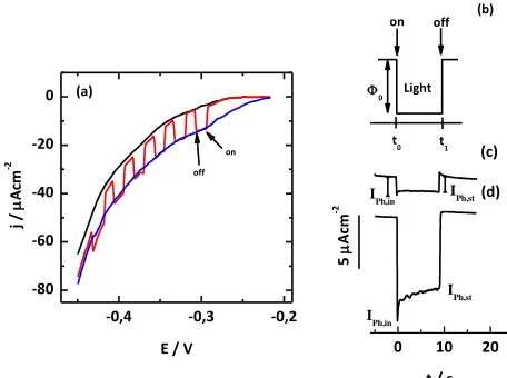
Figure 4a shows potentiodynamic j/E profiles of the Cu2O nanostructures electrodes obtained
[image:5.596.175.422.428.640.2]
It is observed type-p behaviour when the electrode is illuminated in accord with Mott Shottky results (see Fig. 3a). Furthermore, for these electrodes, the photocurrent potential onset (Ebph), is
achieved at a potential value of −0.20 V. However, when considering the respective EFB values, it can
be observed that the overpotential η, (η = Ebph-EFB) attained to -0.438 V value. This relatively high η
value could be explained due to the energy requirements for the charge transfer process of the coupling (I / I3
) on this electrode type. On the other hand, the photocurrent under chopped light illumination
presents a value equal to that obtained with continued light illumination and a low level of recombination. This last, is reflected by the low photocurrent decay after each light pulse.
Photocurrent transients (PT) measurements were carried out in order to verify the level of recombination of photogenerated charge carriers, these were realized following the methodology of L. Peter [36]. Figure 4b shows the square wave chopped light perturbation program applied to the Cu2O
photoelectrode employed during this type of PT studies. Figure 4c-d shows the behaviour of experimental photocurrent transient at polarization potential of -0.32 V and -0.36 V, respectively. In the interval between t = 0 and t = 1 a decay of the photocurrent can be observed until to reach a steady state value (jph,st). This stationary current is a balance between the charge transfer and recombination processes.
-0,4 -0,3 -0,2
-80 -60 -40 -20 0
(c) t
0
0
t1
(b) off on
Light
0 10 20
(d)
t / s
5
Acm
-2
IPh,in
IPh,st
IPh,in IPh,st off
j /
Acm
-2
E / V
on
[image:6.596.180.408.359.529.2](a)
Figure 4. (a) Linear scan voltammetry of Cu2O nanostructures electrodes in the dark (black line), with
continuous light illumination (blue line) and under chopped light illumination conditions (red curve). These curves have been recorded at v = 0.010 Vs−1 (b) Light pulse waveform used for photocurrent transient measurements. Photocurrent transients obtained at (c) 0.32V and (d) -0.36V. These results were obtained with Cu2O nanostructures electrodes (sample grown at
same conditions indicated in Fig. 1) in 10 mM KI, 1 mM KI3 in 50 mM Na2B4O7 (pH 9.2)
solution and room temperature. Light intensity 0 = 50.0 mWcm-2.
Table 1. Results obtained for the jph,st/jph,in ratio from the photocurrent transients measurements for the p - Cu2O phase by ultrasound-assisted anodization of copper substrates.
Synthesis Temperature 50°C Synthesis Temperature 75°C
Cu2O Synthesis Conditions
Epol /
V*
jph, in/
Acm-2
jph, st/
Acm-2
jph, st/jph,
in
Cu2O Synthesis Conditions
Epol / V* jph, in/
Acm-2
jph, st/
Acm-2
jph, st/jph,
in
50V
5% -0.32 -2,17 -0,54 0,25
50V
5% -0.32 -12,12 -5,49 0,45
-0.36 -3,44 -2,09 0,61 -0.36 -20,37 -15,91 0,78
10% -0.32 -6.40 -0,82 0,13 10% -0.32 -2,21 -0,92 0,42
-0.36 -7,04 -1,07 0,15 -0.36 -2,29 -1,52 0,66
75V
5% -0.32 -2,00 -0,80 0,40
75V
5% -0.32 -18,10 -5,48 0,30
-0.36 -2,80 -1,03 0,37 -0.36 -19,24 -9,64 0,50
10% -0.32 -3,49 -1,42 0,41 10% -0.32 -2,10 -1,15 0,55
-0.36 -4,86 -2,85 0,59 -0.36 -1,98 -0,72 0,36
100V
5% -0.32 - - -
100V
5% -0.32 -1,97 -1,60 0,81
-0.36 -8,47 -4,52 0,53 -0.36 -10,14 -6,76 0,67
10% -0.32 -2,38 -1,29 0,54 10% -0.32 - - -
-0.36 -2,16 -0,96 0,44 -0.36 - - -
*
Potential value vs Ag/AgClsat (0.197 V vs HNE)
From the analysis of Table 2, it is established that although in general the samples obtained show a relation jph, st / jph, in close to 0.5 or higher, the nanostructures that show a better behaviour like
photocathodes are those obtained at 100V, 75°C and with 5% wt H2O, the above is due to the fact that
they present a higher initial and stationary photocurrent value. In this way, it can be determined that there are more minority carriers (electrons) to be used in the photoreduction of a reaction of interest. The last means that in the Cu2O nanostructures samples assayed the rate of Faradic process is higher
than the rate of the recombination process [33, 39-41]. This could establish that the most of photogenerated charges were used in the photo-reduction process (
-3
I + 2e 3I)
4. CONCLUSIONS
From the above discussion, was obtained Cu2O nanostructures in the experimental conditions
tested. Those grown at 75°C, 100V in ethylene glycol contained 5% wt H2O and 0.5 wt% NH4Cl, were
those with better photoelectrochemical behaviour. However, from the SEM images and the XRD spectrum it was possible to conclude that the polarization times should be less than 900 s. This last, is due to the growth of a film, possibly of CuCl, that is forms at the upper of the Cu2O nanostructures,
covering part of the electrode surface. This could reduce the photoelectrochemical properties of the Cu2O nanotubes formed. On the other hand, the energy band diagram shows that the system
Cu|p-Cu2O|50 mM Na2B4O7 (pH 9.2) could be pontentially employed as photocathode in the hydrogen
evolution reaction in aqueous solutions
2 2
H O/ H sat
(E - 0.8 V vs Ag / AgCl ) .
ACKNOWLEDGEMENTS
References
1. R. Vijaya Kumar, R. Elgamiel, Y. Diamant, A. Gedanken, Langmuir, 17 (2001) 1406. 2. V. Sáez, T.J. Mason, Molecules, 14 (2009) 4284.
3. J. Bisquert, Phys. Chem. Chem. Phys., 10 (2008) 49.
4. T. Zhang, Z.U. Rahman, N. Wei, Y. Liu, J. Liang, and D. Wang, Nano Res., 10 (2017) 1021. 5. J.G. Lu, P. Chang, Z. Fan, Mat. Sci. Eng. R, 52 (2006) 49.
6. S. Lee, C.-W. Liang, and L.W. Martin, ACS Nano, 5 (2011) 3736.
7. J. Nowotny, C.C. Sorrell, L.R. Sheppard, T. Bak, Int. J. Hydrogen. Energ., 30 (2005) 521. 8. C.N.R. Rao, S.R.C. Vivekchand, K. Biswas, A. Govindaraj, Dalton T., 34 (2007) 3728. 9. N.A. Dhas, C.P. Raj, A. Gedanken, Chem. Mater., 10 (1998) 1446.
10. N.A. Dhas, C.P. Raj, A. Gedanken, Chem. Mater., 10, 3278 (1998).
11. R.V. Kumar, R. Elgamiel, Y. Diamant, A. Gedanken, Langmuir, 17 (2001) 1406. 12. N.A. Dhas, K.S. Suslick, J. Am. Chem. Soc., 127 (2005) 2368.
13. X. Tao, L. Sun, Y. Zhao, Mater. Chem. Phys., 125 (2011) 219.
14. R. Ranjbar-Karimi, A. Bazmandegan-Shamili, A. Aslani, K. Kaviani, Physica B, 405 (2010) 3096. 15. S. Anandan, G.J. Lee, J.J. Wu, Ultrason. Sonochem., 19 (2012) 682.
16. V. Safarifard, A. Morsali, Ultrason. Sonochem., 19 (2012) 823.
17. A. Shui, W. Zhu, L. Xu, D. Qin,Y. Wang, Ceram. Int., 39 (2013) 8715. 18. R.G. Cornpton, J.C. Eklund, F. Marken, Electroanal., 9 (1997) 509.
19. S.K. Mohapatra, M. Misra, V.K. Mahajan, K.S. Raja, J Catal., 246 (2007) 362. 20. V. Mancier, A.L. Daltin, D. Leclercq, Ultrason. Sonochem., 15 (2008) 157. 21. S.K. Mohapatra, S.E. John, S. Banerjee, M. Misra, Chem. Mater., 21 (2009) 3048. 22. Z. Zhang, Md.F. Hossain, T. Takahashi, Mater. Lett., 64 (2010) 435.
23. L.-X. Sang, Z.Y. Zhang, C.F. Ma, Int. J. Hydrogen. Energ., 36 (2011) 4732.
24. L.-X. Sang, Z. Zhi-Yu, B. Guang-mei, D. Chun-xu, M. Chong-fang, Int. J. Hydrogen. Energ., 37 (2012) 854.
25. P. Sakkas, O. Schneider, S. Martens, P. Thanou, G. Sourkouni, Chr. Argirusis, J. Appl. Electrochem., 42 (2012) 763.
26. J. González-García, V. Sáeza, M.D. Esclapeza, P. Bonetea, Y. Vargas, L. Gaete, Phys. Procedia, 3 (2010) 117.
27. S.K. Mohapatra, M. Misra, V.K. Mahajan, K.S. Raja, Mater. Lett., 62 (2008) 1772. 28. T.J. LaTempa, X. Feng, M. Paulose, C.A. Grimes, J. Phys. Chem. C, 113 (2009) 16293.
29. R. Schrebler, L.A. Ballesteros, H. Gómez, P. Grez, R. Córdova, E. Muñoz, R.A. Schrebler, J.R. Ramos-Barrado, and E.A. Dalchiele, J. Electrochem. Soc., 161 (2014) H903.
30. J.G. Lu, P. Chang, Z. Fan, Mat. Sci. Eng. R, 52 (2006) 49.
31. G. Li, Y. Huang, Q. Fan, M. Zhang, Q. Lan, X. Fan, Z. Zhou, C. Zhang, Ionics, 22 (2016) 2213. 32. Q. Pan, M. Wang, J. Electrochem. Soc., 155 (2008) A452.
33. P. Grez, F. Herrera, G. Riveros, R. Henríquez, A. Ramírez, E. Muñoz, E.A. Dalchiele, C. Celedón, R. Schrebler, Mater. Lett., 92 (2013) 413.
34. S. Wu, Z. Yin, Q. He, X. Huang, X. Zhou, and H. Zhang, J. Phys. Chem. C, 114 (2010) 11816. 35. Md. A. Hossain, R. Al-Gaashani, H. Hamoudi, M.J. Al Marri, I.A. Hussein, A. Belaidi, B.A.
Merzougui, F.H. Alharbi, N. Tabet, Mat. Sci. Semicon. Proc., 63 (2017) 203. 36. L.M. Peter, J Solid State Electr., 17 (2013) 315.
37. P. Salvador, J. Phys. Chem., 89 (1985) 3863.
38. P. Salvador, M.L. García-González, and F. Muñoz, J. Phys. Chem., 96 (1992) 10349.
40. F.V. Herrera, P. Grez, R. Schrebler, L.A. Ballesteros, E. Muñoz, R. Córdova, H. Altamirano, and E.A. Dalchiele, J. Electrochem. Soc., 157 (2010) D302.
41. R.S. Schrebler, H. Altamirano, P. Grez, F.V. Herrera, E.C. Muñoz, L.A. Ballesteros, R. A. Córdova, H. Gómez, and E.A. Dalchiele, Thin Solid Films, 518 (2010) 6844