Int. J. Electrochem. Sci., 13 (2018) 5612 – 5619, doi: 10.20964/2018.06.27
International Journal of
ELECTROCHEMICAL
SCIENCE
www.electrochemsci.org
Short Communication
Effects of Electroformed Fe-Ni Substrate Textures on
Light-trapping in Thin Film Solar Cells
Minsu Lee1, Jinho Ahn2*, and Tai Hong Yim1*
1
Surface R&D group, Korea Institute of Industrial Technology, 156 Gaetbeol-ro, Incheon, 21999, Republic of Korea
2
Department of Materials Science and Engineering, Hanyang University, Seoul, 04763, Republic of Korea
*
E-mail: [email protected], [email protected]
Received: 23 February 2018 / Accepted: 5 April 2018 / Published: 10 May 2018
Electroforming can be used to separate electrodeposited metal from the surface of a metal or other conductive material to produce new metallic products with fine shapes. Because Si thin-film solar cells possess fewer absorption layers than other compound thin-film solar cells, light-trapping technology is required to increase the rate of light absorption. Various metal substrate shapes can be constructed in the electroforming process, depending on the shape of the mandrel surface. The objective of this study was to construct specific textured substrates through electroforming to improve light-trapping efficiency in silicon (Si) thin-film solar cells. We constructed pyramid- and V-shaped substrates at angles of 30°, 45°, and 60° by electroforming. To observe the reflective properties of the manufactured substrates, we used an ultraviolet/visible (UV/Vis) spectrometer to measure the total and diffused reflectance. We found that an increase in the contact angle due to changing texture led to a decrease in total reflectance in Fe–Ni alloy substrates. We concluded that substrate texture led to an increase in the light paths in the light-absorbing layers of the thin-film solar cells.
Keywords: Electroforming, Fe-Ni alloy, Light-trapping, Textured substrate, Thin film solar cell
1. INTRODUCTION
these alloys, new methods to directly improve efficiency through the application of developed substrates in thin-film solar cells have been discovered.
In general, the conversion efficiency of thin-film solar cells can be significantly improved by enhancing light absorption in the active layer. Among the many types of solar cells, thin-film solar cells have a thinner active layer. In particular, in Si thin-film solar cells, light-trapping techniques that exploit texture structures are important because they increase the light path through the active layer [13–16]. Nano imprint technology using polyethylene terephthalate (PET), metal foil, and nanorod and nanoparticle methods have been proposed to produce these textures, resulting in an increase in thin-film solar cell conversion efficiency [17, 18]. Thus, the objective of this study was to construct specific textured substrates through electroforming to improve light-trapping efficiency in Si thin-film solar cells. We constructed pyramid- and V-shaped textured substrates, which have good light absorption properties. We also examined different electroforming methods to produce these textured substrates, as well as their reflectance properties.
2. EXPERIMENTAL
2.1. Fabrication of mandrel for electroforming process
Figure 1. Titanium-plated mandrels with 60° contact angles in (a) V-shape and (b) pyramid-shape designs.
2.2. Electroforming process
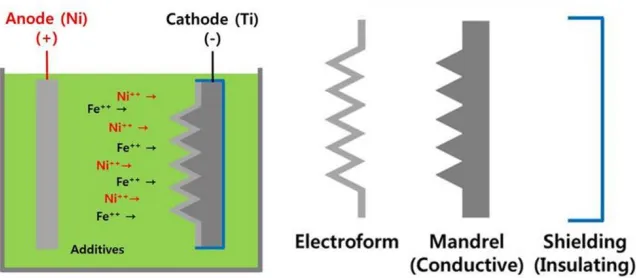
We used 0.1 M iron(II) chloride, 0.6 M nickel(II) sulfamate, 0.5 M boric acid, 0.05 M sodium saccharin, and 0.005 M ascorbic acid as electrolytes to produce the electroformed metal substrate of the thin-film solar cell. The electroforming bath was maintained at 55°C; pH was maintained at 3.5 by adding sulfuric acid. During the electroforming process, we used a general batch-type bath and performed mechanical stirring using paddles. An S-Round Ni anode (Inco Co.) was placed in a Ti basket of the same size as a cathode. A constant current was supplied using a rectifier (6033A; Agilent) with a current density in the range of 40–60 mA/cm2. Figure 2 briefly shows the electroforming process for texture formation. The target thickness of the textured substrate was 50 μm and the current was applied for 50 minutes.
Figure 2. The principle behind the electroforming process used to produce textured substrate in this study.
[image:3.596.93.508.71.214.2] [image:3.596.145.463.497.636.2]3.1. Formation of the Fe–Ni alloy substrate with texture
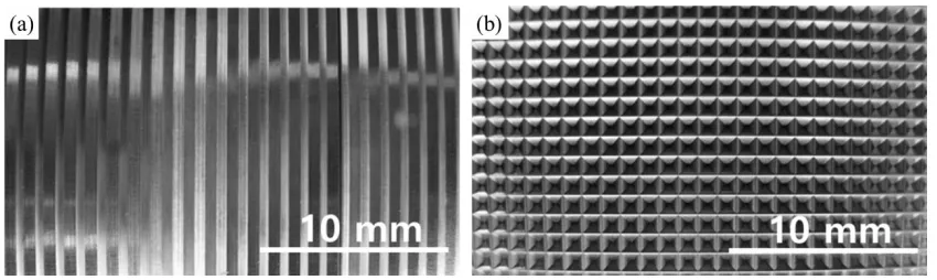
[image:4.596.89.514.431.558.2]Figure 3 shows a sample of the Fe–Ni alloy with electroformed V- and pyramid-shaped textures at a contact angle of 45°. We successfully produced a substrate with uniform texture using the Fe–Ni alloy electroforming technique, constructing a material with the same texture as the mandrel. Figure 4 shows a cross-section of a sample with a contact angle of 60°. To allow easy separation of electroformed substrates from the constructed mandrels, the substrate was treated with chromate using chromic acid anhydride. The natural surface oxide of stainless steel can easily separation of electroformed substrates. Similarly, the chromate layer of titanium mandrel work like natural surface oxide of stainless steel [19, 20]. The pyramid-type texture specimen with a contact angle of 60° did not separate easily at first, but separated easily following chromate treatment.
Figure 3. Optical micrographs (OMs) of textured surfaces on electroformed substrate. (a) V-shape; (b) pyramid-shape.
Figure 4. Cross-sectional OM of the electroformed substrate (facet angle: 60°).
3.2. Reflective properties of the substrate
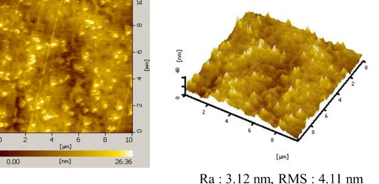
Surface roughness may differ greatly depending on various external variables in the electroforming process, such as current density and the use of additives. It may also affect measurements of diffused reflectance [22, 24]. Therefore, we measured the surface roughness of a flat surface that had been coated under the electroforming conditions of the current study. Figure 5 shows surface roughness measurements for the coated Fe–Ni alloy (average thickness: 4–5 nm), i.e., much greater uniformity than observed in stainless steel substrates produced by a general rolling process [25]. This excellent surface roughness result can be expected to yield suitable adhesion properties for the manufacture of thin-film solar cells [26]. The electroformed substrates simplify the pre-treatment thin-film deposition process. It is generally known that surface roughness is affected by processing variables during the electroforming process. In particular, it is influenced by current density and the use of additives. Thus, it is possible to manufacture metal substrate with varying surface roughness.
[image:5.596.181.413.67.254.2] [image:5.596.112.485.543.724.2]
200 400 600 800 1000 1200 0
10 20 30 40 50 60 70 80 90 100
Re
flectance
(%
)
Wavelength (nm)
Total Diffuse
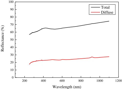
Figure 6. Diffuse and total reflectance spectra for electroformed Fe–Ni substrate (flat shape).
350 400 450 500 550 600 650 700 750 0
20 40 60 80 100
To
tal Refl
ectan
ce (%)
Wavelength(nm)
Pyramid (30°) Pyramid (45°) Pyramid (60°) V-shape (30°) V-shape (45°) V-shape (60°)
[image:6.596.167.417.245.428.2] [image:6.596.170.412.495.677.2]
Figure 7 shows the total reflectance results for pyramid- and V-shaped textured substrates. For both shapes, the total reflectance decreased as the contact angle increased from 30° to 60°, and was lowest for the pyramid-shaped substrate at 60°. The flat Fe–Ni alloy absorbed approximately 40% of the light, reflecting the remaining 60%.
Theoretically, two reflections would cause 36% reflectance and three reflections would cause 21.6% reflectance. Our total reflectance measurements by UV/Vis spectrometry were consistent with these theoretical values. Thus, the total distance traveled by light, i.e., the light path, increased with the formation of pyramid- and V-shaped textures in the substrate, improving efficiency in the thin-film solar cells [30-32]. The application of substrates with large contact angles increase the efficiency of the thin film solar cells.
4. CONCLUSIONS
We constructed textured metal substrates through electroforming. We derived the following conclusions about the methods for producing regular textures in metal substrates through an electroforming process. We successfully constructed metal substrates of thin-film Si solar cells with regular texture and contact angles of 30°, 45°, and 60° through electroforming. The coated substrates were easily separated from the mandrels following chromate treatment on the cathode plate, and substrates with a uniform texture smaller than 1 mm were formed when the cathode plate was fabricated. The reflectance results for the produced substrates showed that light absorption was highest at a contact angle of 60°. We also found that the pyramid-shaped texture absorbed more light than the V-shaped texture. In conclusion, to increase light absorption in thin-film solar cells, the application of substrates with large contact angles is adequate, and may increase the efficiency of the cells.
ACKNOWLEDGMENTS
This work was performed under the support from the R&D Convergence Program of National Research Council of Science & Technology of Republic of Korea (CAP-16-10-KIMS).
References
1. T. Hart and A. Watson, Met. Fin., 97 (1999) 388.
2. A. Purnama, A. Mostavan, C. Paternoster and D. Mantovani, Advances in Metallic Biomaterials, Springer, (2015) Berlin, Heidelberg.
3. D. Zhu, Z.W. Zhu and N.S. Qu, CIRP Ann.-Manuf. Techn., 55 (2006) 193.
4. B. Jiang, C. Weng, M. Zhou, H. Lv and D. Drummer, J. Cent. South. Univ. T., 23.10 (2016) 2536. 5. H. Rho, M. Park, S. Lee, S. Bae, T.W. Kim, J.S. Ha and S.H. Lee, Nanoscale, 8.25 (2016) 12710. 6. M. Weinmann, O. Weber, D. Bähre, W. Munief, M. Saumer, H. Natter, Int. J. Electrochem. Sci., 9
(2014) 3917.
7. M. Lee, Y. Han, H. Um, B.H. Choe and T.H. Yim, J. Renew. Sustain Ener., 6.4 (2014) 042008. 8. S.N. Kumar, R. John, S. Lauer, W. Little and B. Daul, SID Int. Symp. Dig. Tec., 46 (2015) No. 1 9. G. Chatzipirpiridis, O. Ergeneman, J. Pokki, F. Ullrich, S. Fusco, J.A. Ortega, K. M. Sivaraman,
B.J. Nelson and S. Pané, Adv. Healthc. Mater., 4.2 (2015) 209.
20.H. Abe, T. Nakata and T. Watanabe, Mater. Trans., 48.8 (2007) 2165. 21.H. Yang and S.W. Kang, Int. J. Mach. Tool Manu., 40.7 (2000) 1065.
22.E.P. Schmitz, S.P. Quinaia, J.R. Garcia, C.K. de Andrade and M.C. Lopes, Int. J. Electrochem. Sci., 11 (2016) 983.
23.P.C. Andricacos, C. Arana, J. Tabib, J. Dukovic and L.T. Romankiw, J. Electrochem. Soc., 136(5) (1989) 1336.
24.M. Saitou, Int. J. Electrochem. Sci., 10(7) (2015) 5639.
25.B. Ma, A.K. Tieu, C. Lu and Z. Jiang, J. Mater. Process. Technol., 125 (2002) 657. 26.F. Kessler and D. Rudmann, Sol. Energy, 77(6) (2004) 685.
27.N. Ahmad, J. Stokes, N.A. Fox, M. Teng and M.J. Cryan, Nano Energy, 1.6 (2012) 777.
28.S.M. Iftiquar, J. Jung, C. Shin, H. Park, J. Park, J. Jung, J. Yi, Sol. Energy Mater. Sol. Cells, 132 (2015) 348.
29.J. Escarre, F. Villar and M. Fonrodona, Sol. Energy Mater. Sol. Cells, 87 (2005) 333. 30.F.J. Haug and C. Ballif, Enrg. Eviron. Sci., 8(3) (2015) 824.
31.V. Jovanov, E. Moulin, F.J. Haug, A. Tamang, S.I. Bali, C. Ballif and D. Knipp, Sol. Energy Mater. Sol. Cells, 160 (2017) 141.