Int. J. Electrochem. Sci., 8 (2013) 606 - 620
International Journal of
ELECTROCHEMICAL
SCIENCE
www.electrochemsci.orgHigh Performance GdTi
xO
yElectrolyte-Insulator-Semiconductor pH Sensor and Biosensor
Jim-Long Her1, Min-Hsien Wu2, Yen-Bo Peng3, Tung-Ming Pan3,*, Wen-Hui Weng4, See-Tong Pang5, Lifeng Chi6
1
Division of Natural Science, Center for General Education, Chang Gung University, Taoyuan 333, Taiwan, R. O. C.
2
Graduate Institute of Biochemical and Biomedical Engineering, Chang Gung University, Taoyuan 333, Taiwan, R. O. C.
3
Department of Electronics Engineering, Chang Gung University, Taoyuan 333, Taiwan, R. O. C.
4
Department of Chemical Engineering & Biotechnology, Institute of Biotechnology, National Taipei University of Technology, Taipei 10608, Taiwan, R. O. C.
5
Division of Urology, Chang Gung Memorial Hospital, Taiyuan 333, Taiwan, R. O. C.
6 Institute of Physics, Westfälische Wilhelms-Universität Münster, 48149 Münster, Germany *
E-mail: [email protected]
Received: 23 October 2012 / Accepted: 26 November 2012 / Published: 1 January 2013
In this paper, we report an electrolyte–insulator–semiconductor (EIS) device incorporating Gd2O3 and
GdTixOy sensing films deposited on Si substrates through reactive radio frequency sputtering for
biomedical engineering applications. We employed X-ray diffraction, X-ray photoelectron spectroscopy, and atomic force microscopy to investigate the structural and morphological features of these films with annealing at various temperatures. Compared with Gd2O3 sensing membrane, the EIS
device featuring GdTixOy sensing membrane annealed at 900 °C exhibited a higher sensitivity (64.13
mV/pH in the solutions from pH 2 to 12), a smaller hysteresis voltage (1 mV in the pH loop 747107), and a lower drift rate (0.4 mV/h in the pH 7 buffer solution). This outstanding pH sensitivity may be attributed to the high surface roughness of sensing film. Finally, we successfully demonstrated the use of EIS with glucose oxidase-immobilized alginate film for the detection of glucose in serum. The concentration of serum glucose measured by a GdTixOy EIS biosensor is
comparable to that determined by commercial assay kit. The GdTixOy glucose biosensor can detect
glucose with reasonable sensitivity (8.37 mV/mM) in solutions containing glucose at concentrations in the range 0.5–6 mM; this sensitivity is adequate for general clinical examination of blood glucose.
1. INTRODUCTION
The ion–selective field–effect transistors (ISFETs) have been used popularly as biochemical and pH sensors since they were first demonstrated by Bergveld in 1970’s [1-3]. Electrical potential produced by ions at the oxide–electrolyte interface modulates the current in the ISFET’s channel, which is similar to the operating mechanism of the traditional metal–oxide–semiconductor field–effect transistors (MOSFETs). The MOSFET device consists mainly of the metal, oxide, semiconductor substrate, and source/drain; the difference between an ISFET and a MOSFET device is that no metal gate electrode is employed in the former. Electrolyte–insulator–semiconductor (EIS) sensor, the counterpart of ISFET, has several advantages over ISFET including less expensive and easier fabrication. The change in the chemical composition of the analyte will induce variation in the electrical surface charge of the capacitive EIS device, consequently modulating the capacitance of the EIS sensor [3]. Therefore, such an EIS sensor is a promising candidate biosensor for evaluating the sensing characteristics of membranes such as pH sensitivity, hysteresis, and drift [4-5].
Because of the high tunneling current, the conventional SiO2 will be no longer suitable for gate
dielectrics when the CMOS transistor is scaled down to nano regime with the effective oxide thickness less than 1nm [6]. The tunneling current directly influences the gate reliability and draws the extra steady state current [7]. To overcome these problems, high dielectric constant (high-) materials with a thicker physical thickness will replace SiO2 as gate dielectrics in the future generation CMOS devices
[6-7]. Rare-earth (RE) oxide film has emerged as one of the most promising high- gate dielectrics to substitute gate oxide SiO2 due to its high dielectric constant, high resistivity, and large bandgap energy
[8-10]. The main concerns of RE oxide films include silicate formation, hygroscopicity, and formation of O vacancies [8]. The formation of RE silicate on Si may occur by Si diffusion from the substrate [11]. The tendency to form silicate decreases with decreasing ionic radii due to volume constraints. The hygroscopicity of RE oxides decreases with decreasing ionic radii and scales inversely with RE electronegativity [12]. Among the RE oxides, Gd2O3 film can be considered for high- gate dielectric
applications because of its lattice match to Si, good thermal stability with Si, and large conduction and valence band offsets [13-14]. To minimize moisture absorption and silicate formation, the addition of Ti or TiO2 into the RE dielectric films can cause improved physical and electrical properties (a thinner
interfacial layer, lower solubility in water, higher capacitance, and lower leakage current) because it reduces the extent of the reaction of the dielectric film with water and Si substrate [15-17]. In this paper, we described the structural and sensing characteristics of Gd2O3 and GdTixOy sensing films
deposited on Si substrates by means of reactive radio frequency (rf) sputtering. We applied X-ray diffraction (XRD) to determine the growth directions and crystallinity of the films, atomic force microscopy (AFM) to monitor the surface morphology of the Gd2O3 and GdTixOy films, and X-ray
photoelectron spectroscopy (XPS) to analyze the chemical structure of the sensing films after annealing at different temperatures. Furthermore, we determined the effect of post-deposition annealing (PDA) treatment on the sensing characteristics (pH sensitivity, hysteresis, and drift) of the Gd2O3 and GdTixOy films. Finally, we demonstrate that the hybrid configuration of a GdTixOy-based
Int. J. Electrochem. Sci., Vol. 8, 2013
608 glucose. The concentration of serum glucose measured by a GdTixOy EIS biosensor is nearly identical
to that determined by commercial assay kit.
2. EXPERIMENTAL
A. Fabrication of EIS pH sensor
EIS devices with Gd2O3 and GdTixOy sensing membranes were fabricated on a 4-in p-type
(100) silicon wafer with a resistivity of 5-10 Ω–cm. Before the deposition of sensing film, the wafer was cleaned with a standard Radio Corporation of America (RCA) process and then immersed in a dilute 1% HF solution for 30 s to remove the native oxide layer. A ~40 nm Gd2O3 film was deposited
on the Si substrate by reactive rf sputtering from a gadolinium oxide target in diluted O2 ambient
(Ar/O2=5 sccm/2 sccm) at a substrate temperature of 27 °C, whereas a ~40 nm GdTixOy film was
deposited by reactive rf cosputtering from both gadolinium and titanium targets in the same diluted O2
condition. All samples were annealed in a rapid thermal annealing under ambient O2 condition at
selected reaction temperature (700~900 °C) for 30 s. The structure and composition of the Gd2O3 and
GdTixOy films after PDA at different temperatures were analyzed by using XRD and XPS. In the XRD
and XPS analysis, Cu K (=1.542 Å) radiation and monochromatic Al K (1486.7 eV) source are used, respectively. The surface roughness of Gd2O3 and GdTixOy films was measured using AFM in
tapping mode operation. Then, an Al film (~400 nm) was deposited onto the rear of the wafer to act as the backside contact by using thermal evaporation method. The micropatterns on Gd2O3 and GdTixOy
membranes were fabricated by spin-coating a layer of photoresist (SU8-2005 from MicroChem Inc. USA) on the Gd2O3 and GdTixOy films, and by photolithographic processing to define the sensing
zone in Gd2O3 and GdTixOy membranes. The as-fabricated EIS device was attached to printed circuit
board (PCB) with Cu electrode by using a silver gel and then was encapsulated by an epoxy resin. B. pH sensing performance of EIS sensor
Before the pH measurements, EIS device was incubated in reversed osmosis water (R.O.) for 12 h to saturate the ionic properties of the tested sensing membrane. In the pH sensing experiments, the as-fabricated EIS sensor was immersed in various pH buffers (pH 2~12, Merck Inc. USA) together with an Ag/AgCl reference electrode. Capacitance-voltage (C-V) measurements in various pH buffers were performed with Hewlett-Packard (HP) 4284A LCR meter. An ac voltage with the amplitude of 20 mV and the frequency of 100 Hz has been used in all measurements. Moreover, pH sensing experiments were performed in a dark condition to avoid the interference caused by the ambient light and noise.
C. Detection of serum glucose using EIS sensor with enzyme layer
Before the detection of serum glucose, a layer of glucose oxidase-immobilized alginate hydrogel (1 mm) was attached onto the top of GdTixOy sensing film. Briefly, 1X phosphate buffered
chemicals were purchased from Sigma) was thoroughly mixed with an alginate suspension to form a glucose oxidase/alginate suspension with the resulting concentration of 0.1 mg/L. The mixed solution was then loaded onto a clean glass slide and followed by covering with another glass slide with a 1 mm thick spacer in between, allowing the definition of the thickness of alginate thin layer. In the gelatinization process, the sandwich-like structure was incubated in 102 mM CaCl2 solution for 10
min. Finally, the enzyme-containing alginate gel was shaped according to the sensing zone of GdTixOy
sensing film and subsequently attached onto the oxide surface. Glucose standard solutions with different concentrations (0.5~6 mM) were made using 1X PBS and the pH level of each analyte was checked to be equal by a pH meter. In the sensing experiments of glucose, EIS sensor with a layer of enzyme membrane was incubated in the analyte for 10 min and then C-V plot was recorded. The device was thoroughly rinsed with R.O. water after each measurement. For the detection of serum glucose, the serum was firstly diluted 2 times by 1X PBS and the resulting analyte was then examined by a GdTixOy EIS biosensor based on the above-mentioned procedures. Furthermore, the concentration
of diluted serum glucose was also checked by a commercial glucose assay kit (MeDiPro, Taiwan). Briefly, the serum sample was mixed with the assay reagents for 5 min, and then the absorbance of mixed solution was recorded in the wavelength of 505 nm. The concentration of glucose in serum can be determined by comparing its absorbance with the one from standard sample.
3. RESULTS AND DISCUSSION
3.1. Structural properties
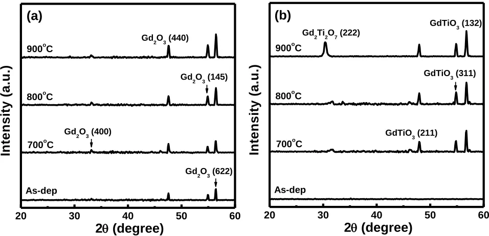
A detailed investigation of the crystalline structure of the Gd2O3 and GdTixOy films before and
after PDA treatment was understood by XRD measurements as shown in Figs. 1(a) and (b). A strong (622) peak and two weak (440) and (145) peaks are observed for the as-deposited Gd2O3 sample,
which means that the film is a polycrystalline structure. In contrast, for the GdTixOy sample, no peak
was found in the 2 diagram, indicating an amorphous structure. The temperature-induced of the crystalline structure of Gd2O3 and GdTixOy films can be followed by XRD analysis. The intensity of
three (440), (145), and (622) diffraction peaks for Gd2O3 film increased with increasing the PDA
temperature, possibly suggesting that the film is condensed during this annealing temperature to form a stoichiometric Gd2O3 film. However, the high temperature annealing will easily produce the formation
of an amorphous silica and/or a nonstoichiometric silicate layer at the oxide/Si interface [8]. In contrast, one strong GdTiO3 (132) peak and two weak GdTiO3 (211) and (311) peaks were found in
the annealed GdTixOy sample, as shown in Fig. 1(b). Besides the peaks mentioned above, the film
annealed at 900 °C had a Gd2Ti2O7 (222) peak in the 2 diagrams, indicative of a preferential
Int. J. Electrochem. Sci., Vol. 8, 2013
[image:5.596.52.530.68.299.2]610
Figure 1. XRD patterns of (a) Gd2O3 and (b) GdTixOy films annealed at various temperatures.
Figure 2. Surface roughness of Gd2O3 and GdTixOy films as a function of PDA temperatures.
The influence of thermal annealing at different PDA temperatures on the surface nature of Gd2O3 and GdTixOy sensing films, the outcome of AFM analysis was showed in Fig. 2. The
as-deposited film exhibited a larger surface roughness than the annealed film. The enhancement in surface
20 30 40 50 60
Gd2O3 (145)
Gd2O3 (400)
(a)
Gd2O3 (622) Gd2O3 (440)
900oC
800oC
700oC
As-dep
In
te
n
s
it
y
(
a
.u
.)
2(degree)
20 30 40 50 60
(b)
GdTiO3 (132)
GdTiO3 (211)
GdTiO3 (311)
900oC
800oC
700oC
As-dep
In
te
n
s
it
y
(
a
.u
.)
2(degree)
Gd2Ti2O7 (222)
0 5 10 15 20 25
0.0 0.2 0.4 0.6 0.8 1.0
GdTi xOy
Gd2O3
As-dep 700 800 900
S
u
rf
a
c
e
r
o
u
g
h
n
e
s
s
(
nm
)
[image:5.596.155.421.387.640.2]
roughness is possibly due to the moisture absorption of RE oxide films leading to the nonuniform volume expansion of the film [18]. The surface roughness of the Gd2O3 and GdTixOy films decreased
with increasing the PDA temperature. We believe that these films are condensed during high temperature annealing as the density increase. In addition, the GdTixOy sample shows a higher surface
roughness compared with the Gd2O3 sample. This is attributed to that the Ti adding into the Gd2O3
[image:6.596.94.501.200.440.2]film increased the growth of the grain size.
Figure 3. XPS spectra of (a) Gd 4d and (b) O 1s for Gd2O3 films annealed at various temperatures.
The effect of the annealing treatment on the compositional properties of the Gd2O3 and
GdTixOy sensing films, XPS analysis was conducted. Figure 3(a) shows the Gd 4d XPS spectra for the
Gd2O3 film after PDA treatment. The Gd 4d3/2 and 4d5/2 peaks of the reference Gd2O3 located at 147.9
and 142.8 eV [19], respectively. It is found that the Gd 4d double peaks of the as-deposited sample are shifted lower binding energy by about 0.5 eV as compared to the Gd2O3 reference position, suggesting
a poor Gd(OH)x structure because of the hydroxide formation after exposure to an air ambient [20].
For the film annealed at 700 and 800 °C, The position of Gd 4d double peaks shifts to a higher binding energy relative to the Gd(OH)x position, suggesting a small amount of Gd reacting with OH causing a
thinner Gd(OH)x. The chemical shift of the Gd 4d doublet peaks moved toward higher binding energy
for the film annealed 900 °C (4d3/2 and 4d5/2 peaks at 147.7 eV and 142.6 eV, respectively) as
compared to the sample annealed 700 and 800 °C. This shift is due to the high Gd-contented metal oxide film. The O 1s spectra for the Gd2O3 films after PDA at different temperatures are shown in Fig.
3(b) with their appropriate peak curve-fitting lines with respect to chemical states. Each fitting peak is assumed to follow the general shape of the Lorentzian-Gaussian function. In four sets of spectra, the O 1s peak at 529.3 eV represents the Gd-O bond [19], the O 1s peak at 531.4 eV assigns to the Gd-O-H bond, and the O 1s peak at 531.6 and 531.8 eV assigns to the Gd-O-Si bond [21]. It is evident that the
152 150 148 146 144 142 140 138 As-dep
In
te
n
s
it
y
(
a
.
u
.)
Binding energy (eV)
700oC Gd2O3
800oC 900oC 4d3/2 4d5/2
(a) Gd
536 534 532 530 528 526 As-dep
In
te
n
s
it
y
(
a
.
u
.)
Binding energy (eV)
700oC 800oC 900oC
Int. J. Electrochem. Sci., Vol. 8, 2013
612 as-deposited film has only O 1s peak at 531.4 eV corresponding to Gd-(OH). This finding indicates that the reaction of Gd2O3 film with water causes the hydroxide formation in the Gd2O3 film. The O 1s
peak intensity corresponding to Gd2O3 increased with increasing the PDA temperature. This finding is
attributed to the reaction of oxygen with Gd atom forming a Gd2O3 structure. On the other hand, the
shift of the O 1s peak (Gd silicate) for the sample annealed at 900 °C to a higher binding energy was increased by 0.2 eV. This is possibly due to the diffusion of oxygen atom from the high-k film to the Gd2O3/Si interface, resulting in the formation of a thicker Gd silicate layer.
Figure 4. XPS spectra of (a) Gd 4d, (b) Ti 2p, and (c) O 1s for GdTixOy films annealed at various
temperatures.
Figure 4 shows the Gd 4d, Ti 2p, and O 1s core level XPS spectra for the GdTixOy films
annealed at different PDA temperatures. The binding energy of Gd 4d3/2 and 4d5/2 peaks at 148.7 and
143.7 eV can be assigned to the Gd2Ti2O7 structure. The chemical shift to higher binding energy for
Gd 4d double peaks indicates the difference between the Gd-O-Ti bonding in Gd2Ti2O7 and that in
Gd2O3. For the as-deposited sample, the Gd 4d3/2 and 4d5/2 peaks at 147.8 and 142.9 eV, respectively,
suggest a poor crystal structure. It is found that the shift of the Gd 4d double peaks for annealed sample to a higher binding energy increases with increasing the PDA temperature. This can be explained by the formation of a better crystal structure during high temperature annealing. For the film annealing at 900 °C, the chemical shift of the Gd 4d double peaks moved toward high binding energy for the case of the GdTixOy film (4d3/2 and 4d5/2 peaks at 148.5 and 143.5 eV, respectively). It should
be noted that the peak of the Ti 2p1/2 and 2p3/2 energy levels appeared at 464.9 and 458.9 eV for the
as-deposited film [Fig. 4(b)], respectively, indicating a poor crystal structure incorporating Ti in the form of TiOH, which probably formed in the surface region of the sample during its exposure to air [12].
For the film annealed at 900 °C, the Ti 2p doublet (Ti 2p1/2 and Ti 2p3/2 at 465.9 and 460 eV,
152 150 148 146 144 142 140 138 As-dep
In
te
n
s
it
y
(
a
.
u
.)
Binding energy (eV)
700oC Gd2O3 Gd2Ti2O7
800oC 900oC 4d3/2 4d5/2 (a) Gd
468 466 464 462 460 458 456 As-dep
In
te
n
s
it
y
(
a
.
u
.)
Binding energy (eV)
700oC 800oC 900oC
TiO2 Gd2Ti2O7
2p3/2 2p1/2
(b) Ti
536 534 532 530 528 526 As-dep
In
te
n
s
it
y
(
a
.
u
.)
Binding energy (eV)
700oC Gd2Ti2O7
GdTiO3
800oC 900oC
[image:7.596.24.573.215.457.2]
respectively) is shifted to higher binding energy compared to the Gd2Ti2O7 reference position (Ti 2p1/2
and Ti 2p3/2 at 465.2 and 459.4 eV, respectively) [22]. This shift was attributed to Ti in GdTixOy
compound consisting of Gd2Ti2O7 and GdTiO3. Figure 4(c) displays the O 1s spectra with appropriate
curve-fitting of peaks for the GdTixOy films after PDA treatment. In the four sets of spectra, the O 1s
peaks at 529.3, 530.1, 531.2, and 532.5 eV represent the Gd–O (Gd2O3), Gd–O–Ti (GdTiO3), Gd–O–
Ti (Gd2Ti2O7), and Gd–O–Si (GdSixOy) bonds [21-22], respectively. The as-deposited film exhibited
one weak Gd silicate and three strong Gd2Ti2O7 GdTiO3, and Gd2O3 peaks, suggesting a poorly
crystalline structure. The O 1s peak intensity corresponding to Gd2O3 decreased with increasing the
PDA temperature, whereas the O 1s peak intensity with respect to Gd2Ti2O7 increased accordingly.
This phenomenon is consistent with the reaction of O and Gd atoms with Ti atoms, forming a well-crystallized Gd2Ti2O7 film. Furthermore, the O 1s peak intensity corresponding to GdTiO3 remained
rather constant for annealed sample. This result is in good agreement with the XRD data showing several intensive diffraction peaks. The O 1s peak corresponding to the Gd silicate components of the film annealed at 800 °C had higher intensity compared to 700 °C, suggesting that Gd atoms diffused from the oxide film to form a thicker Gd silicate layer at the oxide–Si interface.
3.2. Sensing characterization
The reference voltage (VREF) related to the surface potential () depends on the acido-basic
properties of the sensing film and the electrolyte pH. The value of can be determined from the equation 1
) (
1 303
.
2 pH pH
q kT
pzc
………eq. 1
where k is Boltzmann’s constant, T is the temperature of the system, q is the elementary charge, pHpzc is the pH at the point of zero charge, and is a parameter that indicates the chemical sensitivity
of the gate oxide. The pHpzc of pH-ISFET is given by the equation 2
5 . 0
10
log
b a pzc
K K
pH ……….. eq. 2
where Ka and Kb denote the equilibrium constants at acid and base point, respectively. In
addition, the value is related to the chemical sensitivity of gate oxide and is determined by the density of surface hydroxyl groups, which is given as the equation 3.
DL b a s kTC
K K N q2 2
Int. J. Electrochem. Sci., Vol. 8, 2013
614 where Ns is the total number of surface site per unit area and CDL is the double layer
capacitance derived from the Gouy-Chapman-Stern model [23]. In pH-EIS sensing, the change in the pH of the solution caused a shift in the reference voltage of the C–V curves.
Figure 5. C-V curves response of (a) Gd2O3 and (b) GdTixOy EIS devices with annealing at 900 °C
when inserted into solutions with pH values from 2 to 12. The inset shows the reference voltage of (a) Gd2O3 and (b) GdTixOy EIS devices with annealing at 900 °C as a function of pH values.
This result is mainly due to the ionization of the surface hydroxyl groups by either hydrogen ions or hydroxyl ions. The effect of the PDA temperature on the pH sensitivity of the Gd2O3 and
GdTixOy sensing films can be realized by using the site-binding model to describe the ionic absorption
processes at the electrolyte/oxide interface [24].
Figures 5(a) and (b) demonstrate the pH dependence of one group of C–V curves for the Gd2O3
and GdTixOy EIS devices annealed at 900 °C. These normalized C–V curves were shifted as a result of
H+ ions modifying the surface potential through dipole formation on the sensing membrane. This EIS device has distorted C–V curves in the solutions from pH 2 to 12. This may be attributed to the presence of interface traps in the oxide. A set of C-V curves was measured as a function of different pH solutions to determine the pH sensitivity of the sensing film. The inset of Fig. 5(a) and (b) displays the reference voltage (the voltage required to achieve a normalized capacitance of 0.5) of Gd2O3 and
GdTixOy sensing membranes after PDA at 900 °C as a function of pH, respectively. During a cycle
from pH 2 to 12, such a GdTixOy EIS device exhibits a higher pH sensitivity of 64.13 mV/pH
compared with Gd2O3 EIS device.
To evaluate the sensing performance of the Gd2O3 and GdTixOy EIS devices after PDA at
different temperatures, we recorded a set of C–V curves at the pH ranging from pH 2 to 12. The pH
-1.0 -0.5 0.0 0.5
0.2 0.4 0.6 0.8 1.0 Gd 2O3
(a)
pH2 pH4 pH6 pH8 pH10 pH12N
o
rm
a
li
z
e
d
c
a
p
a
c
it
a
n
c
e
Substrate bias (V)
2 4 6 8 10 12
-0.6 -0.4 -0.2 0.0 VR E F ( V ) pH value S=59.63 mV/pH R2 =0.99951
-0.5 0.0 0.5 1.0 1.5
0.2 0.4 0.6 0.8 1.0 GdTi xOy
(b)
pH2 pH4 pH6 pH8 pH10 pH12N
o
rm
a
li
z
e
d
c
a
p
a
c
it
a
n
c
e
Substrate bias (V)
2 4 6 8 10 12
[image:9.596.26.568.157.398.2]
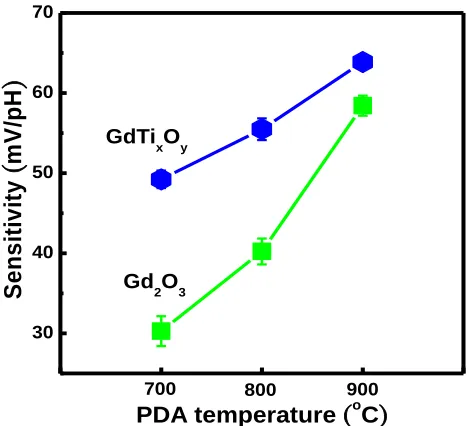
sensitivity of Gd2O3 and GdTixOy EIS devices as a function of PDA temperatures is shown in Fig. 6.
The pH sensitivity of EIS device increases with increasing the PDA temperature. In addition, GdTixOy
[image:10.596.164.400.158.371.2]EIS device exhibits a higher pH sensitivity than Gd2O3 EIS one.
Figure 6. pH sensitivity as a function of PDA temperatures for high- Gd2O3 and GdTixOy EIS devices.
Figure 7. Drift characteristics as a function of times for (a) Gd2O3 and (b) GdTixOy EIS devices
annealed at various temperatures, measured in the pH= 7 solution.
0 5 10 15 20
30 40 50 60 70
Gd
2O3
GdTixOy
700 900
S
e
n
s
it
iv
it
y
(
m
V
/p
H
)
PDA temperature (oC)
800
10-2 10-1 100 101 102
100
101
102
103
Gd2O3
0.60 mV/hr
0.75 mV/hr
0.68 mV/hr (a)
700oC
800oC
900oC
V R
E
F
(
m
V
)
Time (hr)
10-2 10-1 100 101 102
100
101
102
103
GdTixOy
0.64 mV/hr 0.56 mV/hr 0.40 mV/hr (b)
700oC
800oC
900oC
V R
E
F
(
m
V
)
[image:10.596.26.560.446.693.2]Int. J. Electrochem. Sci., Vol. 8, 2013
616
Figure 8. Hysteresis characteristics of (a) Gd2O3 and (b) GdTixOy EIS devices annealed at different
temperatures during the pH loop of 747107.
Figure 9. (a) Scheme of hybrid configuration of a glucose EIS biosensor. The typical calibration curves of (b) GdTixOy EIS glucose biosensor and (c) glucose assay kit.
0 5 10 15 20 25
-0.7 -0.6 -0.5 -0.4 -0.3 -0.2 -0.1 Gd
2O3
pH=7
(a) 700oC
800oC 900oC
pH=10 pH=7 pH=7 pH=4 V R E F ( V ) Time (min)
0 5 10 15 20 25
0.0 0.1 0.2 0.3 0.4 0.5
GdTixOy
pH=7
(b) 700oC
800oC 900oC
pH=10 pH=7 pH=7 pH=4 V R E F ( V ) Time (min) PCB Cu line (Colloidal silver) Al electrode p-type Si
GdTixOy sensing film
SU8
Analyte Reference electrode
Glucose oxidase-immobilized alginate film
Epoxy
SU8
(a)
0 1 2 3 4 5 6 7
-180 -165 -150 -135 -120 -105 1.597 mM (b)
R2=0.98977 VR E F ( m V ) Glucose (mM)
0 1 2 3 4 5 6 7
0.04 0.06 0.08 0.10 0.12 0.14 1.585 mM
R2=0.99943
[image:11.596.48.559.97.331.2] [image:11.596.58.508.419.689.2]
This result could be attributed to the higher surface roughness of the GdTixOy sensing film as
observed in the previous AFM analysis. With the higher surface roughness, the number of surface sites will increase accordingly, which, therefore, contributes to a higher detection sensitivity as previously our discussed in the site-binding model [25]. We find that the GdTixOy sensing membrane annealed at
900 °C has a higher pH sensitivity of 64.13 mV/pH than other PDA temperatures. This result is attributed to the Gd2Ti2O7 and GdTiO3 combining a GdTixOy compound.
Figures 7(a) and (b) show the drift characteristics of Gd2O3 and GdTixOy EIS devices annealed
at various temperatures as a function of time, measured in the pH 7 solutions for 12 h. The drift rate of a pH-ISFET can be explained through the penetration of ions contained in the electrolyte into the sensing membrane [26]. The charged electrolyte ions can penetrate the hydrated layer of the sensing membrane and cause the decrease in effective gate oxide thickness [27]. Therefore, the change of gate capacitance induces the non-ideal effects in the ISFETs. The total amount of penetrating ions and the duration of the penetration process depend on the ion mobility of the sensing membrane. The change in the reference voltage can be written as VREF=VREF(t)-VREF(0). The degradation slope of the reference
voltage variation reflects the stability of an EIS device. The GdTixOy EIS device annealed at 900 °C
exhibited the best long-term stability (slope=0.4 mV/h); in contrast, the Gd2O3 EIS capacitor featured a
high drift of 0.6 mV/h. The small drift effect resulted from the low mobility of ions due to the low density of crystal defects in the film, while a high drift rate is attributed to a larger number of crystal defects producing the high mobility of ions.
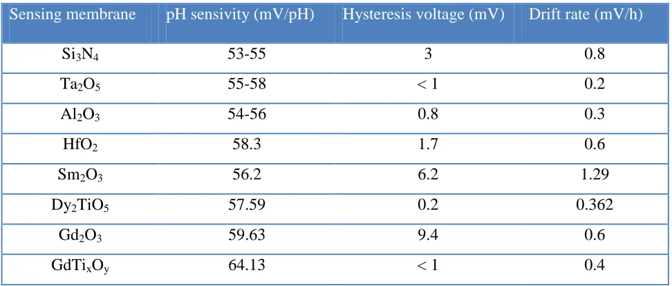
Table 1. Comparison of sensing parameters for an EIS device fabricated with a Si3N4, Ta2O5, Al2O3,
HfO2, Sm2O3, Dy2TiO5, Gd2O3, and GdTixOy.
Sensing membrane pH sensivity (mV/pH) Hysteresis voltage (mV) Drift rate (mV/h)
Si3N4 53-55 3 0.8
Ta2O5 55-58 < 1 0.2
Al2O3 54-56 0.8 0.3
HfO2 58.3 1.7 0.6
Sm2O3 56.2 6.2 1.29
Dy2TiO5 57.59 0.2 0.362
Gd2O3 59.63 9.4 0.6
GdTixOy 64.13 < 1 0.4
Figures 8(a) and (b) depict the hysteresis phenomenon of Gd2O3 and GdTixOy EIS devices
[image:12.596.56.542.450.657.2]Int. J. Electrochem. Sci., Vol. 8, 2013
618 defined as the reference voltage difference between the initial and terminal voltages measured in the above cycle. The EIS device incorporating a GdTixOy sensing film exhibits a smaller hysteresis voltage
than that of Gd2O3 film. This outcome is attributed to the fast response of such a GdTixOy EIS device
due to a better GdTixOy structure and a lower defect chemistry. Furthermore, the GdTixOy EIS device
annealed at 900 °C had a lower hysteresis voltage of ~1 mV than other annealing temperatures. This may be attributed to a low number of crystal defects. In contrast, the 700 °C-annealed sample shows a high hysteresis voltage variation (23 mV), suggesting a large density of crystal defects to create interior sites. These would be sites that can respond to changes of the chemical composition of the tested solution, leading to large variations in the reference voltage.
The measured as well as extracted sensing parameters are summarized in Table 1, where the data from EIS devices incorporating a Si3N4 [29-30], Ta2O5 [31], Al2O3 [29-30], HfO2 [32], Sm2O3
[33], and Dy2TiO5 [34], are shown for comparison. Our present GdTixOy sensing film exhibits superior
better pH sensitivity. Although the GdTixOy EIS device did feature slightly high values of hysteresis
and drift, the thickness of the GdTixOy sensing film can be decreased to lower these values.
3.3. GdTixOy EIS glucose biosensor
In this study, we demonstrated a GdTixOy EIS biosensor with glucose oxidase-immobilized
alginate film to detect directly glucose in serum. Fig. 9(a) illustrates the hybrid configuration of a GdTixOy EIS biosensor. Since the measurement was carried out in serum, a layer of alginate gel could
serve as a filter membrane to possibly avoid the contact of biomolecules with oxide surface, which may prevent unnecessary interference during the detection. Glucose oxidase is a well-known enzyme that catalyzes the oxidation of glucose to yield gluconic acid and hydrogen peroxide while consuming oxygen [35], as described in the reaction.
H D
D
O H D
O H O
D glu eoxidase
gluconoate lactone
glucono
lactone glucono
glucose 2 2 cos 2 2
In the enzymatic reaction of glucose, the amount of gluconic acid is proportional to the concentration of the glucose and the subsequent dissociation of glucose acid generates the hydrogen ions. As a result, the underlying EIS sensor can detect an increase of local pH in the biomembrane upon addition of glucose. Fig. 9(b) demonstrates that the VREF value shows a linear dependence on the
concentration of glucose in the range from 0.5 mM to 6 mM. It is found that the slope of calibration curve of glucose is negative, suggesting that the increase in glucose concentration causes local pH increase near the oxide layer and thus decreases the VREF value of EIS biosensor. Based on the
calibration curve, the sensitivity of a GdTixOy EIS sensor for glucose is about 8.37 mV/mM. It is
diluted by 1X PBS to ensure that the change in the VREF was only induced by the local pH change in
the biomembrane. Furthermore, the dilution treatment allows the buffer capacity of serum is similar to those of standard solutions of glucose [37]. As shown in Fig 9(b), a red circle represents the averaged reference voltages (130.4 mV) from 3 times measurements of serum sample, which also correspond to the serum glucose at a concentration of 1.597 mM. In order to verify the accuracy of a GdTixOy EIS
biosensor, glucose assay kit was used to quantify its concentration in diluted serum and the measured value was directly compared with the one estimated by a GdTixOy EIS biosensor. As shown in Fig
9(c), the standard curve of glucose assay kit displays a good linearity (R2= 0.99) and thus the concentration of glucose in diluted serum can be calculated as 1.585 mM [red circle in Fig. 9(c)]. This concentration level is nearly identical to the value determined by a GdTixOy EIS biosensor with
glucose oxidase immobilized alginate film, suggesting our device is able to accurately quantify the concentration of glucose in serum. Because we demonstrated that a GdTixOy EIS biosensorexhibited
high sensitivity to pH change and the ability of quantifying the biomolecules under a physiological condition, it is expected that this biosensor can potentially serve as the diagnosis tool for general clinical examinations.
4. CONCLUSION
We have developed a highly pH sensitive EIS sensor with a thin layer of Gd2O3 and GdTixOy
by using sputtering technique. We employed XRD, XPS, and AFM analyses to confirm the presence of Gd2O3 and GdTixOy structures in the EIS devices. The GdTixOy EIS device with annealing at 900 °C
exhibited a higher sensitivity (64.13 mV/pH), a smaller hysteresis voltage (1 mV), and a lower drift rate (0.4 mV/h), relative to those of the systems that had been subjected to other annealing conditions. This result is attributed to the combination of Gd2Ti2O7 and GdTiO3 forming a GdTixOy compound and
its higher surface roughness. Finally, we successfully demonstrate the use of GdTixOy EIS with
glucose oxidase-immobilized alginate film for the detection of serum glucose. The GdTixOy EIS
glucose biosensor shows a good linearity (R2 = 0.99) in the concentration range of 0.5-6 mM. Furthermore, the sensitivity of glucose oxidase immobilized EIS biosensor for glucose is about 8.37 mV/mM. The concentration of serum glucose measured by a GdTixOy EIS biosensor is nearly identical
to that determined by commercial assay kit. It is expected that a highly sensitive GdTixOy EIS based
biosensor is promising for the extended application on general clinical diagnosis.
ACKNOWLEDGMENT
This work was supported by the National Science Council, Taiwan, Republic of China, under contract no. NSC-98-2111-E-182-056-MY3.
References
Int. J. Electrochem. Sci., Vol. 8, 2013
620 2. S. V. Dzyadevych, A. P. Soldatkin, A. V. Elskaya, C. Martelet, and N. Jaffrezic-Renault, Anal. Chim.
Acta, 568 (2006) 248.
3. M. J. Schoning and A. Poghossian, Electroanalysis, 18 (2006) 1893. 4. T. M. Pan, C. D. Lee and M. H. Wu, J. Phys. Chem. C, 113 (2009) 21937.
5. J. L. Her, C. W. Lin, K. Y. Chang, and T. M. Pan, Int. J. Electrochem. Sci., 7 (2012) 387. 6. G. D. Wilk, R. M. Wallace, and J. M. Anthony, J. Appl. Phys., 89 (2001) 5243.
7. M. Houssa, High-k Gate Dielectrics, Institute of Physics, London (2004).
8. M. Fanciulli and G. Scarel (Eds.), Rare Earth Oxide Thin Film: Growth, Characterization, and Applications, Springer, Berlin (2007).
9. J. Paivasaari, M. Putkonen, and L. Niinisto, Thin Solid Films, 472 (2005) 275.
10.O. Engstrom, B. Raeissi, S. Hall, O. Buiu, M. C. Lemme, H. D. B. Gottlob, P. K. Hurley, and K. Cherkaoui, Solid State Electron., 51 (2007) 622.
11.H. Ono and T. Katsumata, Appl. Phys. Lett., 78 (2001) 1832. 12.S. Jeon and H. Hwang, J. Appl. Phys., 93 (2003) 6393.
13.M. H. Cho, D. W. Moon, S. A. Park, Y. S. Rho, Y. K. Kim, K. Jeong, C. H. Chang, J. H. Gu, J. H. Lee, and S. Y. Choi, Appl. Phys. Lett., 84 (2004) 678.
14.A. Laha, E. Bugiel, H. J. Osten and A. Fissel, Appl. Phys. Lett., 88 (2006) 172107. 15.R. B. van Dover, Appl. Phys. Lett., 74 (1999) 3041.
16.S. Jeon and H. Hwang, Appl. Phys. Lett., 81 (2002) 4856. 17.T. M. Pan and C. H. Lu, Thin Solid Films, 519 (2011) 8149.
18.Y. Zhao, M. Toyama, K. Kita, K. Kyuno, and A. Toriumi, Appl. Phys. Lett., 88 (2006) 072904. 19.Y. A. Teterin and A. Y. Teterin, Russ. Chem. Rev., 71 (2002) 347.
20.Y. Zhao, K. Kita, K. Kyuno, and A. Toriumi, Appl. Phys. Lett., 89 (2006) 252905.
21.J. F. Moulder, W. F. Stickle, P. E. Sobol, and K. D. Bomben, Handbook of X-Ray Photoelectron Spectroscopy: A Reference Book of Standard Spectra for Identification and Interpretation of XPS Data, Physical Electronics, Eden Prairie, MN (1995).
22.J. Chen, J. Lian, L. M. Wang, R. C. Ewing, and L. A. Boatner, Appl. Phys. Lett., 79 (2001) 1989. 23.R. E. G. van Hal, J. C. T. Eijkel, and P. Bergveld, Sens. Actuators B, 24 (1995) 201.
24.C. D. Fung, P. W. Cheung, and W. H. Ko, IEEE Trans. Electron Devices, 33 (1986) 8.
25.T. M. Pan, K. Y. Chang, C. W. Lin, S. W. Tsai, and M. H. Wu, Sen. Actuators B, 160 (2011) 850. 26.C. C. Wen, T. C. Chen, and J. N. Zemel, IEEE Trans. Electron Devices, 26 (1979) 1945.
27.L. Bousse, S. Mostarshed, B. van der Schoot, and N. F. de Rooij, Sens. Actuators B, 17 (1994)157. 28.L. Bousse, H. H. van den Vlekkert, and N. F. de Rooij, Sens. Actuators B, 2 (1990) 103.
29.Y. Miao, J. Guan, and J. Chen, Biotechnol. Adv., 21 (2003) 527.
30.T. Matsuo, M. Esashi, and H. Abe, IEEE Trans. Electron Devices, 26 (1979). 31.A. Poghossian and M. J. Schoning, Electroanalysis, 16 (2004) 1863.
32.C. M. Yang, C. S. Lai, T. F. Lu, T. C. Wang, and D. G. Pijanowska, J. Electrochem. Soc., 155 (2008) J326.
33.M. H. Wu, C. H. Cheng, C. S. Lai, and T. M. Pan, Sen. Actuators B, 138 (2009) 221. 34.T. M. Pan and C. W. Lin, J. Phys. Chem. C, 114 (2010) 17914.
35.B. R. Eggins, Chemical Sensors and Biosensors, John Wiley & Sons, New York (2002). 36.A. P. Soldatkin, A. V. Elskaya, A. A. Shulga, L. I. Netchiporouk, A. M. Nyamsi Hendji, N.
Jaffrezic-Renault, and C. Martelet, Anal. Chim. Acta, 283 (1993) 695.