Rochester Institute of Technology
RIT Scholar Works
Theses Thesis/Dissertation Collections
7-2015
Dynamic Voltage and Frequency Scaling for
Wireless Network-on-Chip
Pratheep Joe Siluvai Iruthayaraj
Follow this and additional works at:http://scholarworks.rit.edu/theses
This Thesis is brought to you for free and open access by the Thesis/Dissertation Collections at RIT Scholar Works. It has been accepted for inclusion in Theses by an authorized administrator of RIT Scholar Works. For more information, please [email protected].
Recommended Citation
Dynamic Voltage and Frequency Scaling for Wireless
Network-on-Chip
by
Pratheep Joe Siluvai Iruthayaraj
A Thesis Submitted in Partial Fulfillment of the Requirements for the Degree of Master of Science in Computer Engineering
Supervised by
Dr. Amlan Ganguly
Department of Computer Engineering Kate Gleason College of Engineering
Rochester Institute of Technology Rochester, NY
July 2015
Approved By:
_____________________________________________ ___________ ___
Dr. Amlan Ganguly
Primary Advisor – R.I.T. Dept. of Computer Engineering
_ __ ___________________________________ _________ _____
Dr. Dhireesha Kudithipudi
Secondary Advisor – R.I.T. Dept. of Computer Engineering
_____________________________________________ ______________
Dr. Reza Azarderakhsh
ii
Dedication
I would like to dedicate this thesis to my parents Mr. Irudayaraj and Mrs. Regina Rosi who
have supported me from the beginning of this journey. I would also like to dedicate this to
iii
Acknowledgements
I take this opportunity to express my profound gratitude and deep regards to my primary
advisor Dr. Amlan Ganguly for his exemplary guidance, monitoring and constant
encouragement throughout this thesis. Dr. Amlan dedicated his valuable time to review my
work constantly and provide valuable suggestions which helped in overcoming many
obstacles and keeping the work on the right track. I would like to express my deepest
gratitude to Dr. Dhireesha Kudithipudi and Dr. Reza Azarderakhsh for sharing their
thoughts and suggesting valuable ideas which have had significant impact on this thesis. I
am grateful for their valuable time and cooperation during the course of this thesis. I also
take this opportunity to thank my research group members for all the constant support and
iv
Abstract
Previously, research and design of Network-on-Chip paradigms where mainly
focused on improving the performance of the interconnection networks. With emerging
wide range of low-power applications and energy constrained high-performance
applications, it is highly desirable to have NoCs that are highly energy efficient without
incurring performance penalty. In the design of high-performance massive multi-core
chips, power and heat have become dominant constrains. Increased power consumption
can raise chip temperature, which in turn can decrease chip reliability and performance and
increase cooling costs.
It was proven that Small-world Wireless Network-on-Chip (SWNoC) architecture
which replaces multi-hop wireline path in a NoC by high-bandwidth single hop long range
wireless links, reduces the overall energy dissipation when compared to wireline
mesh-based NoC architecture. However, the overall energy dissipation of the wireless NoC is
still dominated by wireline links and switches (buffers).
Dynamic Voltage Scaling is an efficient technique for significant power savings in
microprocessors. It has been proposed and deployed in modern microprocessors by
exploiting the variance in processor utilization. On a Network-on-Chip paradigm, it is more
likely that the wireline links and buffers are not always fully utilized even for different
applications. Hence, by exploiting these characteristics of the links and buffers over
different traffic, DVFS technique can be incorporated on these switches and wireline links
v
In this thesis, a history based DVFS mechanism is proposed. This mechanism uses
the past utilizations of the wireline links & buffers to predict the future traffic and
accordingly tune the voltage and frequency for the links and buffers dynamically for each
time window. This mechanism dynamically minimizes the power consumption while
substantially maintaining a high performance over the system. Performance analysis on
these DVFS enabled Wireless NoC shows that, the overall energy dissipation is improved
vi
Table of Contents
Dedication ... iiAcknowledgements ... iii
Abstract ... iv
Table of Contents ... vi
List of Figures ... viii
List of Tables ...x
Chapter 1 Introduction ...1
1.1. Network-on-Chip (NoC)... 2
1.2. Dynamic Voltage Frequency Scaling (DVFS) ... 4
1.3. Motivation ... 7
1.4. Thesis Contribution ... 8
Chapter 2 Related Work ...11
Chapter 3 Wireless NoC Architecture ...13
3.1. Small World Topology ... 14
3.2. Flow Control and Routing ... 16
3.3. Wireless Interface ... 18
3.4. Antenna and Transceiver ... 19
3.5. Performance Metrics ... 20
3.6. Performance Evaluation ... 22
Chapter 4 Dynamic Voltage Frequency Scaling for WiNoC ...26
vii
4.2. History-based DVFS... 29
4.2.1 Network Traffic Characteristics ... 29
4.2.2 History-based DVFS Policy ... 33
4.2.3 DVFS Controller and Hardware Implementation ... 35
4.3. Performance Evaluation of DVFS-enabled WiNoCs ... 37
4.3.1 Energy Dissipation Characteristics ... 37
4.3.2 Bandwidth and Latency Characteristics ... 39
Chapter 5 Conclusion and Future Work ...43
viii
List of Figures
Fig. 1: Network-on-Chip Architectures [19]. (a) SPIN, (b) CLICHÉ, (c) Torus, (d) Folded torus, (e) Octagon, (f) BFT ... 4Fig. 2: VF variations in a DVFS System [35] ... 5
Fig. 3: Architecture for small-world WiNoC ... 15
Fig. 4: Network Switch with virtual channels ... 17
Fig. 5: (a) On-chip metal zig-zag antenna (reproduced from [3]) (b) On-chip antenna placement on the die (reproduced from [23]) ... 20
Fig. 6: Bandwidth characteristics of mesh and SWNoC... 23
Fig. 7: Latency characteristics of mesh and SWNoC ... 24
Fig. 8: Energy characteristics of mesh and SWNoC... 25
Fig. 9: DVFS Mechanism on Switches and Links ... 27
Fig. 10: Power gate transistor width versus processor performance [56] ... 28
Fig. 11: Utilization profile for uniform traffic (a) Link Utilization profile (b) Buffer Utilization profile ... 32
Fig. 12: Voltage and Delay Curve ... 34
Fig. 13: Finite State Machine for DVFS Controller ... 35
Fig. 14: Total Network Energy for different NoC Architectures... 38
Fig. 15: Total Network Energy for Map-reduced traffic ... 39
Fig. 16: Utilization profile for Map-reduced traffic (a) Link Utilization profile (b) Buffer Utilization profile ... 40
ix
Fig. 18: Bandwidth characteristics for Map-reduced traffic ... 41
Fig. 19: Latency characteristics for different architectures ... 42
x
List of Tables
Table 1: Voltage/Frequency/Threshold Combinations………34
1
Chapter 1
Introduction
Network-on-Chip (NoC) architectures have become a primary focus for researchers
for designing high performance and energy efficient multicore processors and
System-on-Chip (SoC) architectures that can integrate hundreds of cores in a single chip [1].
Traditional network fabrics suffer from an important performance and power
consumption limitation in designing massive multicore chips, where a data transferred
between two distant cores because high power consumption and latency issues [2].
However, NoCs have been identified to show increased performance by inserting
long-range wired links using the principle of small-world graphs [3]. As the system size
scales up, the small-world topology takes advantage of the inherent multi-hop nature of the
largely separated communicating cores and reduces the average hop count by introducing
a relatively long-distance direct shortcuts. These network fabrics can further be improved
by replacing the single hop long-range wired links with energy efficient, wireless links.
The wireless shortcuts have been shown to carry a substantial amount of traffic, thus
enabling significant energy savings through these low power wireless links.
However, the overall energy savings in the system can further be improved by
optimizing the characteristics of the wireline links and associated switches based on the
data traffic it takes. Dynamic voltage and frequency scaling (DVFS) is a popular technique
that enables power optimization of electronic systems without significantly compromising
the system performance. The required voltage and frequency levels in the DVFS is
optimized based on the traffic pattern generated by the benchmark applications. Mainly
2
savings in processing cores. This paper extends the technique by performing DVFS on
NoC platform by characterizing the voltage and frequency levels based on the utilizations
of each individual links and switches. These DVFS enabled switches and links helps
reducing the energy dissipation of a multi-core chip and consequently provides high energy
savings for a network-on-chip platform.
1.1.
Network-on-Chip (NoC)
One of the major problems in future SOC designs arises from non-scalable delays
in global wires [19]. Global wires carry signals across a chip and typically do not scale in
length with technology scaling [20]. Though gate delays scale down with technology,
global wire delays typically increase exponentially or linearly by inserting repeaters. Even
after repeater insertion [21], the delay may exceed the limit of one or multiple clock cycles.
In ultra-deep submicron processes, it is claimed that 80 percent or more of the delay of
critical paths will be due to interconnects [22]. As a result, many large designs use as hoc
FIFO buffers to synchronously propagate data over large distances to overcome this
problem. According to the ITRS report, “Global synchronization becomes prohibitively
costly due to process variability and power dissipation, and cross-chip signaling can no
longer be achieved in a single clock cycle.” [23]. Thus, system design must work on
networking and distributed computation paradigms with functional blocks integrated into
the communication backbone. The most frequently used on-chip interconnect architecture
is an arbitrated bus, where all communication devices share the same transmission medium.
Advantages of such shared-bus architectures are simple topology, low area and
3
can be quite high. Moreover, every additional IP block added to the bus adds to this
parasitic capacitance, in turn increasing propagation delay. As the bus length and/or the
number of IP blocks increases, the associated bit transfer delay over the bus becomes large
and will 3 eventually exceeds the targeted clock period. This places a limit on the number
of IP blocks that can be connected to a bus and thereby limits the system scalability [24].
One solution to deal with this problem is to split the bus into multiple segments and employ
a hierarchical architecture [25]; however, this is ad hoc in nature and has the inherent
limitations of the bus-based architecture. In SoCs consisting of several IP blocks, bus-based
interconnects will face serious bandwidth problems as all attached devices must share the
same medium [24]. To overcome the above-mentioned problems, use of a
communication-centric approach to integrate IPs in complex SoCs is advocated. This new model separates
the resource elements (i.e., the IPs) from the communication infrastructure (i.e., the
network). The need for global synchronization thus disappears. This new approach is
explicitly parallel, exhibits modularity to minimize global wires and utilizes locality in
power minimization [26]. In a network-centric approach, communication between IPs
happens in the form of packets. A common characteristic of such architectures is that the
IP blocks communicate with each other using intelligent switches or routers. As such, these
switches dubbed infrastructure IPs (I2Ps) [26] provide a robust data transfer medium for
the functional IP modules. There is another manner of explaining the relevance of Network
on Chips [27]. Reliable communication between circuit components requires a protocol
definition that provides some rules describing how the interaction shall take place. These
rules ensure that the overall system performance requirements are met, while physical
4
use ad-hoc 4 approaches that often fail to meet some strict scalability requirement of
next-generation SOC designs. Bottlenecks can arise in performance, throughput, power, energy,
reliability, synchronization, predictability and concurrency Designers traditionally stuck to
point-to-point connections and bus-based techniques. This approach is acceptable for a
[image:15.612.99.512.216.468.2]small number of blocks when the performance/ latency trade-off is relatively simple.
Fig. 1: Network-on-Chip Architectures [19]. (a) SPIN, (b) CLICHÉ, (c) Torus, (d) Folded torus, (e) Octagon, (f) BFT
1.2.
Dynamic Voltage Frequency Scaling (DVFS)
One active area of work on NoC has focused on dynamically varying operating
voltage and frequency levels to achieve a balance between power and performance [29].
This technique, referred to as DVFS, is used quite often in SoC designs [30]. Dynamic
voltage and frequency scaling (DVFS) was introduced in the 90’s [31] to dramatically
5
of the system with respect to changing workloads [32, 33, 34, 35]. Fig. 2 shows the time
varying pattern of voltage and frequency in a system exhibiting DVFS [35]. Alternative
techniques using voltage/frequency islands (VFIs) for IP blocks are used in achieving fine
grain system-level power management [36]. Use of VFIs in the NoC context can provide
better power-performance tradeoffs than single voltage, single clock frequency case as it
benefits from the natural partitioning and mapping of applications onto the NoC platform.
Despite the huge potential for energy savings with 6 VFIs, the NoC design methodologies
considered so far are limited to a single voltage clock domain [37, 38, 39]. Studies that do
consider multiple VFIs assume that each module/core in the design belongs to a different
[image:16.612.112.498.361.578.2]island and different islands are connected by point-to-point (P2P) links [40, 41].
Fig. 2: VF variations in a DVFS System [35]
Power-gating is a standby-leakage reduction method developed in [42, 43, 44, 45,
6
supplies to parts of a design in standby mode [47]. Clock gating was also proposed as a
power saving technique [48, 49, 40]. Some studies indicate that the clock signals in digital
computers consume a large (15–45%) percentage of the system power [51]. Thus, the
circuit power can be greatly reduced by reducing the clock power dissipation. Many clock
power reduction techniques have focused on reduced voltage swings, buffer insertion, and
clock routing [52]. In many cases, switching of the clock causes a huge 7 gate activity. In
circuits with controllable clocks, master clock is used to derive all other clocks which,
based on certain conditions, can be slowed down or stopped completely with respect to the
master clock [53].
In this thesis mainly the DVFS circuits and techniques are applied to each switch
and wireline links in the NoC such that each switch and link is contained in its own
independent clock and voltage domain. Lowering the supply voltage leads to a square
reduction in dynamic power based on the dynamic power-voltage relationship given as,
𝑃𝑑𝑦𝑛 = 𝛼𝐶𝑉2𝑓
Where, α is the switching probability or activity, C is the total load capacitance, Vdd is the
supply voltage, and f is the clock frequency. Without altering the supply voltage, power
can be reduced with frequency reduction, but the energy consumption per operation
remains the same. Supply voltage reduction on the other hand, contributes directly to
energy reduction, where the dynamic energy consumption of a gate is a direct function of
the supply voltage: 𝐸 = 𝐶𝑉𝑑𝑑2. Leakage power is reduced as well with reduced supply voltage under normal circumstances. DVFS becomes increasingly important as leakage
power becomes dominant contribution to power consumption in very deep-submicron
7
and thermal effects [55]. Slower parts of the chip can be speeded up with higher voltages,
and hotter parts can be cooled with lower voltages.
Reduction in supply voltage results in an increased gate propagation delay (td),
𝑡𝑑 = 𝐶𝑉𝑑𝑑/(𝑉𝑑𝑑 − 𝑉𝑡)𝛼
Where, Vt is the threshold voltage, and α is the velocity saturation index. To guarantee
correct operation of a synchronous system, the frequency must normally be scaled along
with the voltage. The performance overhead of frequency and voltage scaling can be
mitigated in a multi-core network-on-chip architecture by taking advantage of the variation
in workloads across the buffers and wireline links in the network. Switches (buffers) can
operate at a higher voltage during periods of high utilization, and at lower voltages during
periods of low utilization to minimize energy dissipation.
1.3.
Motivation
The limitations and design challenges associated with existing NoC architectures
has led to the emergence of Wireless Network-on-Chip, that enables technology to design
high bandwidth and low power multicore architectures[13],[11]. It is shown in [13] that
the network consumes a significant part of the chip’s power budget and it can be almost
50% depending on the application. Most of the existing works related to the design of
wireless NoC demonstrate its advantage in terms of latency and energy dissipation
provided by the wireless channels only. The main emphasis always has been on the
characteristics of the wireless links. However, the overall energy dissipation of the wireless
NoC can be improved even further if the characteristics of the wireline links and buffers
8
Dynamic Voltage Frequency Scaling (DVFS) is known to be an efficient power
management technique. Taking advantage of the characteristics of the wireline links and
buffers in the interconnection network, DVFS can be incorporated for significant energy
savings in Wireless NoC system. This thesis is aimed at implementing DVFS scheme in
the interconnection network of small world wireless NoC system with efficient history
based DVFS controller for wireline links and buffers in the network, for significant energy
savings.
1.4.
Thesis Contribution
In this thesis, it will be demonstrated that by implementing Dynamic Voltage and
Frequency Scaling on interconnection networks for Wireless NoCs with efficient DVFS
controller, significant power savings can be achieved when compared to existing power
management techniques in Wireless NoCs. The history based DVFS technique will be
implemented on wireline links and buffers by taking advantage of the utilization
characteristics over a time window to predict the future utilization and vary the voltage and
frequency accordingly for significant energy savings. This proposed system will prove to
be more energy efficient than previous NoC paradigms. The proposed system is
implemented with other existing topologies and will be evaluated for performance
characteristics and energy savings. Furthermore, the trade-off between performance and
energy will be established for different traffic conditions. The following points will
summarize the contributions made during this work.
9
o Design and implementation of Dynamic Voltage Frequency Scaling for
Wireless NoCs
o Design and development of history-based DVFS controller.
Evaluation of Wireless NoC Schemes
o Evaluation of energy savings over Wireless NoCs and DVFS-enabled
Wireless NoCs
o Evaluation of performance trade-off over DVFS-enabled Wireless
NoCs
o Evaluation of DVFS-enabled Wireless NoCs for different traffic
patterns
Development of simulation framework
o Develop a cycle accurate simulator to implement the wireless NoC
architectures with Dynamic Voltage and Frequency Scaling for wireline
links and buffers.
o Develop an efficient algorithm to implement the DVFS controller for
history based prediction mechanism.
o Obtain experimental results of DVFS-enabled Wireless NoC
architecture with other wired and wireless architectures with respect to
the following parameters using the cycle accurate simulator.
Peak achievable bandwidth
Latency Overheads
Packet energy dissipation
10
Publication
o Nassef Mansoor, Pratheep Joe Siluvai Iruthayaraj, Amlan Ganguly,
“Design Methodology for a Robust and Energy-Efficient
Millimeter-wave Wireless Network-on-Chip”, IEEE Trans. on Multi-Scale
11
Chapter 2
Related Work
Various research groups have investigated power and thermal management of
multicore-based computing platforms. Dynamic voltage and frequency scaling (DVFS) is
a popular methodology to optimize the power usage/heat dissipation of electronic systems
without significantly compromising overall system performance. Hence DVFS can be
applied to multi-core processors; to all cores or to individual cores independently [4].
Multi-core chips implemented with multiple Voltage Frequency Islands (VFI) design styles
are other promising alternatives. VFI is shown to be effective in reducing on-chip power
dissipation [5] [6]. Various research groups have addressed designs of appropriate DVFS
control algorithms for VFI systems [7]. Some researchers have also recently discussed the
practical aspects of implementing DVFS control on a chip, such as tradeoffs between
on-chip verses off-on-chip DC-DC convertors [4], the number of allowed discrete voltage levels,
and centralized verses distributed control techniques [11]. Thermal-aware techniques are
principally related to power-aware design methodologies using DVFS [8]. It is shown that
distributed DVFS provides considerable performance improvement under thermal duress
[8].
Most of the existing works principally address power and thermal management
strategies for the processing cores only. Network consume a significant part of the chip’s
power budget; generally affecting overall temperature. However, there is little research on
how they contribute to the thermal issues [9]. Thermal Herd, proposed in [9], provides a
distributed runtime scheme for thermal management that allows routers to collaboratively
12
minimizing performance impact. For the first time, [10] addressed the problem of
simultaneously dynamic voltage scaling of processors and communication links for the
real-time distributed systems. Intel’s recent multi-core-based single chip cloud computers
(SCC) incorporate DVFS both in the core and the network levels. However, all of the
above-mentioned works principally consider standard multi-hop interconnection
network-levels for the multi-core chips; the limitations of which are well known.
A comprehensive survey regarding various WiNoC architectures and their design
principles are presented in [12]. It is already shown that the small-world network
architecture with long-range wireless shortcuts can significantly improve the energy
consumption and achievable data rate of massive multicore computing platforms [12].
Here, we complement that effort by simultaneously addressing the power and thermal
management of WiNoC-based multi-core processing platforms by incorporating
13
Chapter 3
Wireless NoC Architecture
The earlier interconnect technologies have been used in existing NoC platforms
without significant architectural innovations, which undermines the performance gains.
However, the emerging technologies make direct connections between physically distant
cores on the chip viable due to their high communication bandwidth and low power
dissipation characteristics. This allows innovation in the design of the NoC architecture to
maximize the utilization of the performance benefits of these emerging interconnects,
specifically the wireless communication channels. Many naturally occurring networks are
known to have the so-called small-world property. Networks with the small-world property
have a very short average path length, which is commonly measured as the number of hops
between any pair of nodes. The average shortest path length of small-world graphs is
bounded by a polynomial in log(N), where N is the number of nodes, which makes them
particularly interesting for efficient communication with minimal resources [16, 17]. This
feature of small-world graphs makes them particularly attractive for constructing scalable
WiNoCs. Most complex networks, such as social networks, the Internet, as well as certain
parts of the brain exhibit the small-world property. This makes them scalable with increase
in system size. Thus such connection topologies are suitable for modern multi-core
systems, which have hundreds of cores on a single die. The adopted small-world topology
essentially inserts long-range links in the NoC. However, long wireline interconnects incur
high energy dissipation and latency in data transfer. So as many long-range links as
possible are replaced with wireless interconnects based on the scalable small-world
14
3.1.
Small World Topology
In this type of topology, each core is connected to a NoC switch and the switches
are interconnected using wireline and wireless links. The topology is a small-world
network where the links between switches are established following a power law
distribution as shown below.
ij ij j i ij ij f l f l j i P , (1)
Where, the probability of establishing a link, between two switches, i and j, P(i,j),
separated by an Euclidean distance of lij is proportional to the distance raised to a finite
power [17]. The distance is obtained by considering a tile-based floorplan of the cores on
the die. The frequency of traffic interaction between the cores, fij, is also factored into (1)
so that more frequently communicating cores have a higher probability of having a direct
link. This frequency is expressed as the percentage of traffic generated from i that is
addressed to j. This frequency distribution is based on the particular application mapped to
the overall NoC and is hence known prior to wireless link insertion. Therefore, the apriori
knowledge of the traffic pattern is used to establish the topology with a correlation between
traffic distribution across the NoC and network configuration as in [18]. This optimizes the
network architecture for non-uniform traffic scenarios. The parameter α govern the nature
of connectivity. Higher the value of alpha, lesser the number of longer links which brings
down the total wiring cost for the system. Also, it is established in [17] that choosing a
value of α<D+1, where D is the dimension of the network a small-world network
connectivity can be established. In our case the NoC is arranged in a 2D tile and
15
connectivity [17] for which it also noticed that the system has maximum throughput with
minimum wiring cost. As the links are established probabilistically following (1) the
number of ports of each switch may not be the same. The average number of ports per
switch is however constrained to be 5 to have the total number of connections same as that
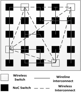
of a mesh. Fig. 1. Shows the small-world WiNoC architecture of 25 core system where
each core is associated with a NoC Switch, connected using wireline links and few long
[image:26.612.136.473.266.653.2]distant cores using wireless links.
Fig. 3: Architecture for small-world WiNoC
NoC Switch
Wireless
Switch
interconnect
Wireline
16
3.2.
Flow Control and Routing
For a conventional NoC system, there can be basically three types of switching that
can be considered for data routing. Namely, Circuit Switching, Packet Switching and
Wormhole Switching.
In case of circuit switched networks, a dedicated path is reserved for the complete
duration of the transmission. Even though the network bandwidth is reserved during the
transmission it is highly inefficient when there are many nodes waiting for transmission
along the same path which eventually degrades the system performance.
In case of packet switching, data is divided into packets and sent over the network
to the destination. Even though there is no reservation of path for transmission, the packets
needs to be buffered in the switches along the path to the destination. In an SOC, this
means more area overhead for the switches which are not acceptable as on-chip silicon real
estate is limited.
In this research work, wormhole switching is adopted wherein packets are divided
into small units called flow control units or flits. The size of flit is chosen such that a single
flit can traverse a single hop in a single clock cycle. These flits are transmitted along the
network across switches .Hence the large buffer requirement for the switches are avoided.
The first flit or the header flit of a packet contains the routing information. This information
enables the switches to setup the path and the rest of the flits follow this path in a pipelined
fashion [2]. But a problem associated with such a switching technique is that distinct
messages cannot be sent over a switch at the same time, as the path would be reserved for
a particular packet till it is completely transmitted. Hence to solve this problem a concept
17
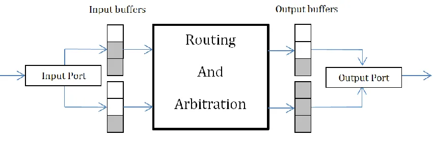
Basically a virtual path is reserved for each distinct message. This is accomplished
by reserving separate buffers for each message in all the switches along the path, forming
a distinct virtual path for each message. Fig. 4 shows a block diagram of how this is
accomplished. Here node A and node B are allocated separate buffers along the path which
enables the switch to receive and send messages from both the nodes, simultaneously using
[image:28.612.95.520.259.399.2]a multiplexer.
Fig. 4: Network Switch with virtual channels
WiNoC has adopted wormhole routing in which data is transferred via flits using
virtual channels (VCs) [14]. WiNoC is essentially an irregular architecture and in irregular
architectures it is important to achieve distributed and deadlock-free routing of data flits.
This is achieved through a layered shortest path routing policy (LASH) [15]. In LASH,
shortest paths between different source-destination pairs are separated into multiple virtual
layers with specific VCs dedicated for each layer. This avoids cyclic dependencies between
paths in a particular layer. Computation of the path for each packet would result in a large
overhead hence, the shortest path between any source and destination is pre-computed
18
corresponding to all possible final destinations. As a result, the memory required to store
the routing table is linearly proportional to system size. When a header flit arrives at a
particular switch the next switch is determined from the routing table based on the final
destination of the packet. The header flit is then routed to the appropriate port along the
particular VC reserved for its source/destination pair. Only the next switch is determined
at each intermediate switch making the routing decision fast and efficient. Since the routing
paths are the shortest paths, high data rates can be achieved with moderate number of VCs
to avoid deadlock [15]. In order to grant access to the wireless channel to multiple WIs in
a distributed manner, token flow control is adopted. Only after all the flits belonging to a
particular packet are transmitted, the token is forwarded to the next WI. Since WIs provide
shorter pats to route packets, many messages would try to access them leading to
congestion. To avoid congestion at the WIs, if no buffer space is available at the wireless
port of a switch then the packet is routed through the shortest available wired path.
3.3.
Wireless Interface
The two important WI components are the antenna and the transceiver. The on-chip
antenna for the mSWiNoC has to provide the best power gain for the smallest area
overhead. A metal zigzag antenna has been demonstrated to possess these characteristics
and hence is used for this work [11]. To ensure high throughput and energy efficiency, the
WI transceiver circuitry has to provide a very wide bandwidth as well as low power
19
3.4.
Antenna and Transceiver
Suitable on-chip antennas are necessary to establish wireless links for WiNoCs. In
[13] the authors demonstrated the performance of silicon integrated on-chip antennas for
intra- and inter-chip communication. They have primarily used metal zig-zag antennas
operating in the range of tens of GHz. Design of an ultra-wideband (UWB) antenna for
inter- and intra-chip communication is elaborated in [19]. This particular antenna was used
in the design of a wireless NoC [9] mentioned earlier in chapter 1. The above mentioned
antennas principally operate in the millimeter wave (tens of GHz) range and consequently
their sizes are on the order of a few millimeters. If the transmission frequencies can be
increased to THz/optical range then the corresponding antenna sizes decrease, occupying
much less chip real estate. Characteristics of metal antennas operating in the optical and
near-infrared region of the spectrum of up to 750 THz have been studied [20]. Antenna
characteristics of carbon nanotubes (CNTs) in the THz/optical frequency range have also
been investigated both theoretically and experimentally [21-22]. Although CNT antennas
will support higher data bandwidth but significant manufacturing challenges need to be
overcome to make them feasible for adoption in mainstream chip fabrication processes.
That is why a metal based CMOS process compatible antenna structure is used in this work
which can be adopted in the near future.
The on-chip antenna for the proposed wireless NoC has to provide the best power
gain for the smallest area overhead. A metal zig-zag antenna [23] has been demonstrated
to possess these characteristics. This antenna also has negligible effect of rotation (relative
angle between transmitting and receiving antennas) on received signal strength, making it
20
used in [3] designed with 10μm trace width, 60μm arm length and 30° bend angle. The
axial length depends on the operating frequency of the antenna. The characteristics of the
antennas are simulated using the ADS momentum tool. High resistivity silicon substrate
(=5kΩ-cm) is used for the simulation. The details of the antenna simulation setup and
antenna structure are shown in Fig. 5(a) [24]. To represent a typical inter-subnet
communication range the transmitter and receiver were separated by 20 mm. The forward
transmission gain (S21) of the antenna obtained from the simulation is shown in Fig. 5(b).
As shown in Fig. 5(b), we are able to obtain a 3 dB bandwidth of 16 GHz with a center
frequency of 57.5 GHz. For optimum power efficiency, the quarter wave antenna needs an
axial length of 0.38 mm in the silicon substrate.
633 µm Silicon Substrate
(εr=11.7)
SiO
2 (εr=3.9)
2 µm
Free Space (εr=1)
Antenna
Dis tan
ce betw een An
ten nas (d
)
60 µm
A x ia l L e n g th 3 0 ° 1 0 µ m
Zig- Zag Antenna
Fig. 5: (a) On-chip metal zig-zag antenna (reproduced from [3]) (b) On-chip antenna placement on the die (reproduced from [23])
3.5.
Performance Metrics
The experiments are carried out using a cycle accurate simulator implementing the
NoC architectures with 3-stage switches namely, input, output arbitrations and routing [2].
[image:31.612.127.477.392.535.2]21
the number of interconnects. As shown in [30] irregular networks of size 64, 128 and 256
cores require 4, 6 and 9 layers for deadlock-free routing. Each layer is considered to have
a single VC reserved. The mesh architecture is considered to have 4 VCs in each input and
output port. Each VC has a buffer depth of 2 flits. A uniform random spatial distribution
of traffic is used for the all experiments. All the NoC components are driven with a 2.5GHz
clock. All simulations are performed for ten thousand cycles allowing for transients to
settle in the first few thousand cycles. If the wireline links are long enough to take more
than 1 clock cycle for transmission of a flit they are pipelined by insertion of FIFO buffers
such that between any two stages it is possible to transfer an entire flit in 1 clock cycle.
The on-chip zig-zag antennas are able to provide a bandwidth of 16GHz around a center
frequency of 60GHz [3] while the transceivers [23] are able to sustain a maximum data
rate of 6Gbps. All the wireless switches are equipped with the same transceivers. We have
considered a flit size of 32 bits and a packet size of 64 flits.
The metrics for performance evaluation are maximum achievable bandwidth and
packet energy dissipation. Maximum achievable bandwidth is the peak sustainable data
rate in number of bits successfully routed per second. Bandwidth, B can be determined as,
𝐵 = 𝑡𝛽𝑁𝑓 (2) Where, t is the maximum throughput in number of flits received per core per clock
cycle at network saturation, is the number of bits in a flit, N is the number of cores in the
NoC and f is the clock frequency. The throughput is directly obtained from system level
simulations performed by the NoC simulator.
The packet energy dissipation, Epkt is the average energy dissipated in transmission
22
𝐸𝑝𝑘𝑡 =(∑ (𝐿𝑖−ℎ𝑖𝜆)𝐸𝑏𝑢𝑓+ℎ𝑖𝐸𝑤𝑖𝑟𝑒𝜆)+𝑁𝑠𝑖𝑚𝐸𝑤𝑖𝑟𝑒𝑙𝑒𝑠𝑠
𝑁𝑝𝑘𝑡 𝑖=1
𝑁𝑝𝑘𝑡 (3)
Where, Npkt is the number of packets routed in the NoC, Liis the latency of the ith
packet, hi is the number of hops in the path of the packet and Ebufis the energy dissipation
of a flit in the NoC switch buffers. The energy dissipation of a wireline hop is Ewireand
is the packet length in number of flits. Nsim is the duration of the simulation and Ewireless is
the energy dissipated by all the wireless transceivers in the WiNoC in one cycle.
3.6.
Performance Evaluation
Experimental Setup:
In this section, a complete evaluation on the basis of bandwidth, latency and energy
dissipation is carried out comparing the wired and wireless network architectures of
SWNoC and mesh-based NoC. GEM5, a full system simulator is used to obtain detailed
network-level information. An 8x8 core network with 64 routers, each with 8 virtual
channels and 16 flit buffers per input port is assumed. Fixed length packets of 64 flits
where, the head flit leading 63 body flits, and each flit being 32-bits wide are assumed.
Similar to the wired links, wireless links are also incorporated with warm-hole routing. The
NoC simulator uses switches synthesized from an RTL level design using TSMC 65nm
CMOS process, using Synopsys Design Vision. Energy dissipation of the network switches
were obtained from the synthesized net-list by running Synopsis Prime Power, while
energy dissipated by wireline links were obtained through HSPICE simulations taking into
consideration length of the wireline links. Each wireless link can sustain data rate of
23 Performance Characteristics:
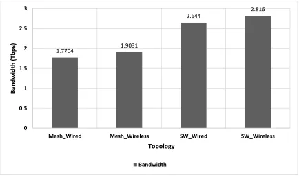
Here, presented is the bandwidth, latency and packet energy profiles of the wired
and wireless implementation of small-world and mesh based NoCs. Fig. 6 shows the
bandwidth characteristics, Fig. 7 shows the latency characteristics and Fig. 8 shows the
energy dissipation profile for different NoC topologies. It can be observed from Fig. 6 that
when comparing traditional mesh based NoCs, small-world topology has better
performance in terms of bandwidth and particularly, small-world with 10 wireless nodes
[image:34.612.90.524.319.576.2]have the superior performance over other implementations.
Fig. 6: Bandwidth characteristics of mesh and SWNoC
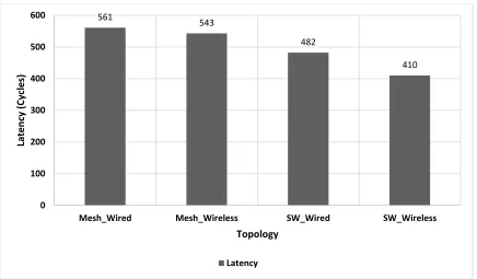
It can be observed from Fig. 7 that for all of the network topologies considered, the
latency of SWNoC is lower than that of the mesh architectures. This is due to the
small-1.7704 1.9031
2.644 2.816
0 0.5 1 1.5 2 2.5 3
Mesh_Wired Mesh_Wireless SW_Wired SW_Wireless
B
an
d
wi
d
th
(Tb
p
s)
Topology
24
world architecture of SWNoC with direct long-range, one-hop wireless links that enables
a smaller average hop-count than that of mesh. With this significant decrease to the overall
latency in the SWNoC architecture, an opportunity is formed to further increase energy
[image:35.612.90.526.207.462.2]savings to match the performance of SWNoC with that of the baseline mesh architectures.
Fig. 7: Latency characteristics of mesh and SWNoC
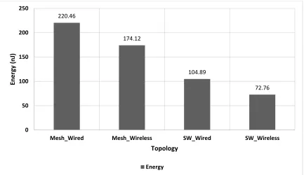
Now, evaluating the energy dissipation characteristics of the mesh and small-world
with wired and wireless counterparts, it is evident that introduction of wireless links in the
topology could avoid energy dissipation of few long range wireline links. In addition, the
small-world topology reduces the multi-hop communication and thus ensures less energy
dissipation due to long range wireline links. Further, by replacing long range wireline links
by wireless links, the energy dissipation is significantly reduced as shown in Fig. 8
561
543
482
410
0 100 200 300 400 500 600
Mesh_Wired Mesh_Wireless SW_Wired SW_Wireless
Late
n
cy
(
Cy
cl
e
s)
Topology
25
Fig. 8: Energy characteristics of mesh and SWNoC
Hence, it was clearly seen from these performance analysis that small-world
wireless network-on-chip architectures significantly improves overall energy dissipation
and performance when compared to mesh-based architectures.
220.46
174.12
104.89
72.76
0 50 100 150 200 250
Mesh_Wired Mesh_Wireless SW_Wired SW_Wireless
En
e
rg
y
(n
J)
Topology
26
Chapter 4
Dynamic Voltage Frequency Scaling for WiNoC
It is established that Small-world Wireless Network-on-Chip is an enabling
architecture to improve power efficiency and performance characteristics of multi-core
architectures. The inherent SWNoC architecture modifies the distribution of network
traffic patterns among network elements significantly. The execution flow of a program on
a multicore NoC generally contains periods of heavy computation followed by periods of
inter-core data exchange. During periods of high computation, network usage may be at a
minimum, allowing the voltage and frequency of links and switches to be tuned down in
order to save energy. Hence, it is possible to vary the voltage and frequency of the SWNoC
switches and links depending on the traffic-dependent bandwidth requirements.
Here in this thesis, a fully distributed fine-grain DVFS is employed on switches and
links, where the ports and links are tuned according to their utilizations following a history
based algorithm that predicts the future traffic characteristics on the network based on what
was seen in the past. The utilization characteristic is chosen to be a relevant metric to
determine whether DVFS should be performed.
4.1.
DVFS Architecture and Modeling
Most DVFS architectures apply only a single DVFS controller to an entire chip
using an on-chip or off-chip DC-DC converter. A fine grain DVFS implementation can
increase the effectiveness of DVFS by tuning the supply voltage to individual parts of the
chip. One way to achieve this is to supply discrete voltages to the chip, and have the
27
Fig. 9 shows a concept diagram of DVFS with five voltage supplies using PMOS
power gates [8]. Current flow through power gate transistors result in a voltage drop that
negatively impacts performance. The amount of voltage drop, VPG, is related to the
dimensions of the power gates: VPG = IPGRPG, where IPG is the current through the power
gates, RPG is directly related to L/W where L and W are the length and width of the power
gate transistors respectively. The voltage drop causes an increase in the power gate’s delay.
Voltage drop can be reduced by making W/L as large as possible, which can be
accomplished by adding power gates in parallel.
To accurately measure the performance loss associated with the power gates, a
precise current profile from the processor core is first obtained with SPICE simulations.
This current waveform is then used to create the voltage drop across the power gates, and
the resulting increase in delay can be measured. In 65nm technology, the relationship
[image:38.612.128.482.430.653.2]between power gate width and performance is shown in Fig.10.
28
Fig. 10: Power gate transistor width versus processor performance [56]
The DVFS controller in Fig. 9 contains the logic to estimate the voltage and
frequency that is required by the buffers and the links. This estimate is obtained based on
the Buffer and Link Utilization values that is obtained from the buffers in the switch. The
decision of voltage and frequency is made using an algorithm that is explained later in
this thesis. Frequency scaling is performed by incrementing or decrementing the clock
frequency based on the utilization information. A range of allowable frequencies is
assigned for each voltage setting which is shown in Table 1, where the setting of Vin are
mapped to settings of Freq_val. Therefore frequency scaling is performed automatically
29
4.2.
History-based DVFS
The mechanism controlling the DVFS has to carefully trade off power and
performance, minimizing the power consumption of the network while maintaining high
performance. Hence, in this thesis a distributed history-based DVFS policy is proposed. In
this policy, the router port predicts future communication workload based on the analysis
of prior traffic, then dynamically adjusts the voltage and the corresponding frequencies of
its buffers and links to accommodate the network load.
4.2.1 Network Traffic Characteristics
Network communication traffic characteristics can be captured with various
network traffic measures. In order to predict the network load based on what was seen in
the past, a suitable indicator has to be explored over a fixed time window. The metric to
determine whether DVFS should be performed is utilization. Tuning a given link and
buffer’s voltage and frequency is determined by the link utilization and buffer utilization
respectively.
Link Utilization
𝐿𝑈 =∑ 𝐹(𝑡)
𝑁 𝑡=1
𝑁 0 < 𝐿𝑈 < 1
Where,
LU is the Link Utilization.
N is the number of clock cycles, which is sampled within a history window size H.
30
Link Utilization is a direct measure of the traffic workload in the links of the
network. First, the number of flits that gets transferred using a particular link is captured
over a time window, then the Utilization is measure as a ratio of total flits transferred to
the number of clock cycles that is sampled within a history time window. Assuming that,
a flit takes one time unit to get transferred over the link. Link utilization can take any value
between 0 and 1. A higher link utilization (>=0.5) reflects that more data are sent to the
next router. As the history is predictive, this indicates a higher link voltage and frequency
is needed to meet the performance requirement. Conversely, lower link utilization (<0.5)
implies the existence of more idle cycles. Hence, decreasing the link frequency can lead to
power savings without significantly affecting performance.
To investigate how the predicted link utilization vary the frequency based on the
predictions, the utilization values and the clock speed is tracked with a two dimensional
8x8 mesh network. Network traffic is generated based on the bench mark traffic patterns,
for this study a uniform traffic pattern was considered. Fig. 10(a) shows the utilization of
a single link as sampled every 100 cycles (H = 100), across the entire timing simulation of
uniform load. It can be seen that at low traffic workloads (LU < 0.5), contention of the link
is less and hence the utilization is lower, correspondingly the operating frequency of the
links is also lowered. When contention starts to build in the link and when the utilization
crosses the threshold 0.5, the link operating frequency is increased and reaches its
maximum operating frequency as work load increases. The graph clearly shows the two
extreme network scenarios of lightly congested and heavily loaded along with its frequency
requirements for DVFS operation. At low network loads, since the flit will not be stalled
31
latency. At high network loads, flits will be stalled in the next router for a long time, hence
getting there faster will not be significant. In this case, link frequency can be decreased
more aggressively with minimum delay constrains. Hence, link utilization alone will not
be sufficient for guiding the history-based DVFS policy. One more measure, input buffer
utilization is investigated.
Input Buffer Utilization
𝐵𝑈 = ∑ (𝐸(𝑡)
𝑁
𝑡=1 /𝐵)
𝐻 0 < 𝐵𝑈 < 1
Where,
BU is the Buffer Utilization
E(t) is the number of VC’s in input buffer that are occupied at time t.
B is the total input buffer size.
Buffer Utilization tracks how many VC’s in each buffer switch are occupied over
a time window. As traffic increases, more flits are stored in the buffers which may lead to
contention and increase in the utilization measure. Buffer utilization is calculated over a
time window as a fraction of number of flits occupied in a buffer to the total capacity of
the buffer. Buffer utilization can take any value between 0 and 1. The input buffer
utilization is tracked downstream from the same link shown in Fig. 10(a) to investigate
how frequency scaling behaves with network traffic and contention. Fig. 10(b) shows the
graph that plots the buffer utilization and the frequency of operation that scales based on
32
(a)
[image:43.612.104.508.72.599.2](b)
Fig. 11: Utilization profile for uniform traffic (a) Link Utilization profile (b) Buffer
Utilization profile 0 0.2 0.4 0.6 0.8 1 1.2 Uti lization & Vo ltage
Time Window (Cycles)
Link Utilization Vs Link Voltage
Link Voltage Utilization 0 0.1 0.2 0.3 0.4 0.5 0.6 0.7 0.8 0.9 1 Uti lization & Vo ltage
Time Window (Cycles)
Buffer Utilization Vs Buffer Voltage
Buffer Voltage
33
4.2.2 History-based DVFS Policy
Network traffic exhibits two dynamic trends: transient fluctuations and long-term
transitions. This history-based DVFS policy filters out short-term traffic fluctuations and
adapts link frequencies and voltages carefully to traffic transitions. This is carried out by
sampling link and input buffer utilization within a fixed history window and using the
exponential weighted average utilization to combine current and past utilizations history.
Algorithm 1:
Assume that initially, 𝐿𝑈𝑝𝑎𝑠𝑡 = 1 & W = any finite number.
𝑓𝑜𝑟 𝑒𝑎𝑐ℎ(𝑡𝑖𝑚𝑒 𝑤𝑖𝑛𝑑𝑜𝑤) 𝑏𝑒𝑔𝑖𝑛
𝐿𝑈𝑝𝑟𝑒𝑑𝑖𝑐𝑡𝑒𝑑 = (𝑊 ∗ 𝐿𝑈𝑐𝑢𝑟𝑟𝑒𝑛𝑡 + 𝐿𝑈𝑝𝑎𝑠𝑡)/(𝑊 + 1)
𝐿𝑈𝑝𝑎𝑠𝑡 = 𝐿𝑈𝑝𝑟𝑒𝑑𝑖𝑐𝑡𝑒𝑑
𝐵𝑈𝑝𝑟𝑒𝑑𝑖𝑐𝑡𝑒𝑑 = (𝑊 ∗ 𝐵𝑈𝑐𝑢𝑟𝑟𝑒𝑛𝑡 + 𝐵𝑈𝑝𝑎𝑠𝑡)/(𝑊 + 1)
𝐵𝑈𝑝𝑎𝑠𝑡 = 𝐵𝑈𝑝𝑟𝑒𝑑𝑖𝑐𝑡𝑒𝑑
𝐿𝑖𝑛𝑘𝑉𝑜𝑙𝑡 = 1𝑣
𝐵𝑢𝑓𝑓𝑒𝑟𝑉𝑜𝑙𝑡 = 1𝑣
𝑇ℎ𝑟𝑒𝑠ℎ𝑜𝑙𝑑𝑉𝑜𝑙𝑡 = 0.5𝑣
𝑖𝑓(𝐿𝑈𝑝𝑟𝑒𝑑𝑖𝑐𝑡𝑒𝑑 < 𝑇ℎ𝑟𝑒𝑠ℎ𝑜𝑙𝑑𝑉𝑜𝑙𝑡 && 𝐿𝑖𝑛𝑘𝑉𝑜𝑙𝑡 < 1)
𝐿𝑖𝑛𝑘𝑉𝑜𝑙𝑡 = 𝐿𝑖𝑛𝑘𝑉𝑜𝑙𝑡 + 0.1
𝑒𝑙𝑠𝑒𝑖𝑓(𝐿𝑈𝑝𝑟𝑒𝑑𝑖𝑐𝑡𝑒𝑑 >= 𝑇ℎ𝑟𝑒𝑠ℎ𝑜𝑙𝑑𝑉𝑜𝑙𝑡 && 𝐿𝑖𝑛𝑘𝑉𝑜𝑙𝑡 > 0.5)
𝐿𝑖𝑛𝑘𝑉𝑜𝑙𝑡 = 𝐿𝑖𝑛𝑘𝑉𝑜𝑙𝑡 − 0.1
𝑒𝑛𝑑
𝑖𝑓(𝐵𝑈𝑝𝑟𝑒𝑑𝑖𝑐𝑡𝑒𝑑 < 𝑇ℎ𝑟𝑒𝑠ℎ𝑜𝑙𝑑𝑉𝑜𝑙𝑡 && 𝐵𝑢𝑓𝑓𝑒𝑟𝑉𝑜𝑙𝑡 < 1)
𝐵𝑢𝑓𝑓𝑒𝑟𝑉𝑜𝑙𝑡 = 𝐵𝑢𝑓𝑓𝑒𝑟𝑉𝑜𝑙𝑡 + 0.1
𝑒𝑙𝑠𝑒𝑖𝑓(𝐵𝑈𝑝𝑟𝑒𝑑𝑖𝑐𝑡𝑒𝑑 >= 𝑇ℎ𝑟𝑒𝑠ℎ𝑜𝑙𝑑𝑉𝑜𝑙𝑡 && 𝐵𝑢𝑓𝑓𝑒𝑟 𝑉𝑜𝑙𝑡 > 0.5)
𝐵𝑢𝑓𝑓𝑒𝑟𝑉𝑜𝑙𝑡 = 𝐵𝑢𝑓𝑓𝑒𝑟𝑉𝑜𝑙𝑡 − 0.1
𝑒𝑛𝑑
34
Given the predicted communication link utilization LUpredicted and input buffer
utilization BUpredicted, the DVFS policy dynamically adapts its voltage scaling and
frequency scaling to achieve power savings with minimal impact on performance. It
determines whether to increase link voltage and frequency to the next higher level, decrease
link voltage and frequency to the next lower level, or do nothing. So, when a link is going
to be highly utilized, voltage frequency scaling is carried out to handle load. Similarly, if a
link is mostly idle, DVFS is carried out to save power. Otherwise, voltage frequency
scaling is conservatively carried out to minimize impact on performance. The states
depends on five voltage and frequency levels shown in Table 1. The pseudo-code of the
proposed DVFS policy is shown in Algorithm 1. The threshold voltage 0.5v is chosen
based on the plot shown in Fig.12. Since beyond 0.5v there much increase in delay which
[image:45.612.163.451.431.611.2]can considerably affect the system performance.
35
4.2.3 DVFS Controller and Hardware Implementation
The proposed DVFS policy relies only on local link and buffer utilizations
information. This avoids communication overheads in relying global information, and
permits a simple hardware implementation. To measure link utilization, a counter at each
output port gathers the total number of cycles that are used to relay flits in each history
interval. Another counter captures the ratio between the router and link clocks. A simple
multiplier combines these two counters to calculate the link utilization. Most
interconnection network routers use credit-based flow control. Current buffer utilization is
already available. Two registers store LUpast and BUpast, which feed the circuit module
calculating the exponential weighted average. Finally some combinational logic performs
the threshold comparisons and outputs signal that control the DVFS links and buffers.
Fig. 11 shows the finite state machine that was built inside the controller to switch
between different voltage and frequency levels based on the utilization values of the link
and buffers. Where, LU specifies Low Utilization (Utilization < 0.5) and HU specifies High
[image:46.612.95.516.497.606.2]Utilization (Utilization >= 0.5).
36
Table 1: Voltage/Frequency/Threshold Combinations
States Voltage (Volts) Frequency (GHz)
Normal 1 2.5
OPT 1 0.9 2.25
OPT 2 0.8 2
OPT 3 0.7 1.75
OPT 4 0.6 1.5
OPT 5 0.5 1.25
The DVFS controller were synthesized from RTL level design using 65nm
standard cell libraries from CMP [23], using Synopsys. The delay, area and power
numbers are shown in Table 2. The controller results with an area of about 300 equivalent
logic gates per router port. As the circuit does not lie on the critical path of the router, its
delay can be ignored. With power estimation for the circuit, it was found that the power
[image:47.612.87.526.523.640.2]overhead is negligible which approximately 100nW per router port.
Table 2: DVFS Controller in Overall System metrics
DVFS Controller
Power 15.332µW(~2% of Overall Chip)
Area 44850µm2 (~3% of Overall Chip)
37
4.3.
Performance Evaluation of DVFS-enabled WiNoCs
This section evaluates the performance of the history-based DVFS policy with
conservative DVFS enabled wireline links and input buffers on a NoC environment. With
the same experimental setup as explained in chapter 3, considering a buffer depth of 16
and 8 virtual channels, the DVFS enabled NoC architectures are evaluated by studying the
trade-off between network latency/throughput degradation and dynamic power savings.
One of the key goals of this thesis is to uncover the effect of DVFS enabled links and input
buffers on network power and performance, providing insights that will guide future design
of DVFS enabled Wireless NoCs.
4.3.1 Energy Dissipation Characteristics
This subsection presents the network-level energy dissipation of the SWNoC by
incorporating the DVFS technique described earlier. For completeness, the characteristics
of the conventional wireline and wireless mesh architecture incorporating DVFS technique
is shown.
Fig. 12 shows the network energy dissipation for the various architectures for 16
buffer depth and 8 virtual channels. It can be observed from Fig. 12 that among different
architectures, the network energy is much lower for the SWNoC. The two main
contributors of the energy dissipation are the switches and the interconnect infrastructure,
In the SWNoC, the overall switch energy decreases significantly compared to mesh as a
38
Fig. 14: Total Network Energy for different NoC Architectures
In this case, the hop count decreases significantly, and hence, on an average, packets have
to traverse through less number of switches and links. In addition, a significant amount of
traffic traverses through the energy efficient wireless channels in SWNoC; consequently
decreasing the interconnect energy dissipation. With the addition of DVFS, total network
energy can be further reduced. As the traffic traversing through the wireline links is heavily
reduced in the SWNoC, the opportunity for implementing DVFS is significant. From Fig.
12 it is clear that DVFS-enabled SWNoC saves 40% of energy with respect to the
Non_DVFS SWNoC implementation.
Fig. 13 shows the network energy savings on DVFS-enabled SWNoC architecture
for different traffic benchmarks. It is clear that for different traffic patterns, the
DVFS-enabled SWNoC architecture can still provide approximately 40% savings in energy
dissipation for all traffic patterns.
220.46
174.12
104.89
72.76 136.74
110.35
60.19
45.65
0 50 100 150 200 250
Mesh_Wired Mesh_Wireless SW_Wired SW_Wireless
En
ergy
(n
J)
Packet Energy
39
Fig. 15: Total Network Energy for Map-reduced traffic
4.3.2 Bandwidth and Latency Characteristics
This section accounts the bandwidth and latency penalty for implementing DVFS
mechanism on NoC architectures. Fig. 14 shows the peak achievable bandwidth for NoC
architectures with and without DVFS. It is clear that there is bandwidth penalty with the
dynamic voltage scaling on wired and wireless system regardless. However, the penalty
that is to be accounted for is only 3-4% of the peak bandwidth that was achieved without
implementing DVFS. The difference in bandwidth is mainly due to the fact that the links
and input buffers are switched between different voltages and frequency values. The
bandwidth reduction is the penalty for frequent switching characteristics of the DVFS
policy. Fig.16 clearly shows the voltage fluctuations that does not follow the predictions
because of the smaller steps. Hence there is bandwidth and latency limitations for different
traffic patterns. 173.72 188.1 193.56 208.7 167.64 195.3 106.37 127.19 114.7 127.12 101.76 119.56 0 50 100 150 200 250
Histogram Kmeans Linear
Regression
Matrix Multiplication
PCA Word Count
E ne rgy ( nJ )
Energy for Different Traffic Patterns
40
(a)
[image:51.612.103.508.71.595.2](b)
Fig. 16: Utilization profile for Map-reduced traffic (a) Link Utilization profile (b) Buffer
Utilization profile 0 0.2 0.4 0.6 0.8 1 1.2 Uti lization & Vo ltage
Time Window (Cycles)
Link Utilization Vs Link Voltage
Link Voltage Utilization 0 0.2 0.4 0.6 0.8 1 1.2 Uti lization & Vo ltage
Time Window (Cycles)
Buffer Utilization Vs Buffer Voltage
Buffer Voltage
41
Fig. 17: Bandwidth characteristics for different architectures
This degradation will not be a dominant concern when there is 40% energy
reduction in the system. Still the DVFS-enabled small-world wireless performance is better
than the small-world wired implementation. In low-power applications, 3-4% performance
compromise is acceptable with 40% energy savings
Fig. 18: Bandwidth characteristics for Map-reduced traffic
1.7704 1.942 2.7494 2.8902 1.7034 1.8391 2.6882 2.7924 0 0.5 1 1.5 2 2.5 3 3.5
Mesh_Wired Mesh_Wireless SW_Wired SW_Wireless
Ban d w id th (T b p s)
Bandwidth
Without-DVFS With-DVFS 2.457 2.5492.797 2.852 2.669
2.484
2.312 2.461
2.609 2.752 2.618
2.447 0 0.5 1 1.5 2 2.5 3
Histogram Kmeans Linear
Regression
Matrix Multiplication
PCA Word Count
B an dw idth ( T bp s )
Bandwidth for Different Traffic Patterns
[image:52.612.122.491.470.657.2]42
Latency penalty is not very significant as shown in Fig. 15. However, the latency
is high in few architectures because of slowing down of the links and buffers by frequency
scaling, where one flit takes 2 cycles to be transfers from one link to another instead of 1
flit per cycle. Hence, there is a negligible amount of increase in cycles in few NoC
architectures. However, the DVFS-enabled SWNoC shows very less change in the latency
numbers which still proves to be a better architecture for maintain the desired frequency
[image:53.612.106.508.265.431.2]with significant amount of energy savings.
Fig. 19: Latency characteristics for different architectures
Fig. 20: Latency characteristics for Map-reduced traffic
561 529 382 359 577 535 412 375 0 200 400 600 800
Mesh_Wired Mesh_Wireless SW_Wired SW_Wireless
La ten cy (Cy cle s)
Latency
Without-DVFS With-DVFS 432 421 416 397 429 427 447 439 425 412 438 433 370 380 390 400 410 420 430 440 450 460Histogram Kmeans Linear
Regression
Matrix Multiplication
PCA Word Count
La ten c y ( Cy c les )
Latency for Different Traffic Patterns
[image:53.612.118.487.486.652.2]43
Chapter 5
Conclusion and Future Work
In this thesis, it is demonstrated that how a small-world DVFS-enabled wireless
network-on-chip improves the energy dissipation of a multi-core chip. By adopting a
small-world interconnection infrastructure, where long distance communications will be
predominantly achieved through high performance specialized single hop wireless links,
communications can be made significantly more energy efficient. To further extend the
energy savings, implementing network level DVFS on wireline links and input buffers, a
significant energy savings can be achieved. Just as DVFS in microprocessors exploits the
variance in processor utilization to tune processor voltage and frequencies
![Fig. 1: Network-on-Chip Architectures [19]. (a) SPIN, (b) CLICHÉ, (c) Torus, (d) Folded torus, (e) Octagon, (f) BFT](https://thumb-us.123doks.com/thumbv2/123dok_us/90105.8483/15.612.99.512.216.468/network-chip-architectures-spin-cliche-torus-folded-octagon.webp)
![Fig. 2: VF variations in a DVFS System [35]](https://thumb-us.123doks.com/thumbv2/123dok_us/90105.8483/16.612.112.498.361.578/fig-vf-variations-in-a-dvfs-system.webp)
![Fig. 5: (a) On-chip metal zig-zag antenna (reproduced from [3]) (b) On-chip antenna placement on the die (reproduced from [23])](https://thumb-us.123doks.com/thumbv2/123dok_us/90105.8483/31.612.127.477.392.535/fig-chip-metal-antenna-reproduced-antenna-placement-reproduced.webp)

![Fig. 10: Power gate transistor width versus processor performance [56]](https://thumb-us.123doks.com/thumbv2/123dok_us/90105.8483/39.612.125.478.81.349/fig-power-gate-transistor-width-versus-processor-performance.webp)