Rochester Institute of Technology
RIT Scholar Works
Theses Thesis/Dissertation Collections
4-2012
An Industrial Fluid Multi-Sensor
Nicholas O. Liotta
Follow this and additional works at:http://scholarworks.rit.edu/theses
This Thesis is brought to you for free and open access by the Thesis/Dissertation Collections at RIT Scholar Works. It has been accepted for inclusion in Theses by an authorized administrator of RIT Scholar Works. For more information, please [email protected].
Recommended Citation
i
An Industrial Fluid Multi-Sensor
A Thesis Submitted in Partial Fulfillment of the
Requirements for the Degree of
Master of Science in Electrical Engineering
By
Nicholas O. Liotta
Approved by:
__________________________________________ Date_________________ Dr. Lynn F. Fuller (Thesis Advisor)
__________________________________________ Date_________________ Dr. Sergey E. Lyshevski (Thesis Committee Member)
__________________________________________ Date_________________ Dr. Ivan Puchades (Thesis Committee Member)
__________________________________________ Date_________________ Dr. Sohail A. Dianat (Chair Electrical and Microelectronic Engineering)
DEPARTMENT OF ELECTRICAL AND MICROELECTRONIC ENGINEERING KATE GLEASON COLLEGE OF ENGINEERING
ROCHESTER INSTITUTE OF TECHNOLOGY ROCHESTER, NEW YORK
ii
Acknowledgments
I would like to thank Dr. Fuller for his guidance and support throughout my
Thesis. I have learned a great deal from you. Thanks for teaching me so much about
Microelectronics. I would like to thank Dr. Lyshevski for his mentorship during my time
at RIT and for being on my Thesis committee. Thank you for always pushing me in your
classes to reach my full potential. I would like to thank Dr. Puchades for his help
troubleshooting, pushing me to understand everything, and always being there to answer
any questions along the way. I would like to thank Dan Smith for always being willing to
help and teach me things I did not know before. It has been a lot fun working with you. I
would like to thank Luis Gan for his help and friendship. I would like to thank Clare for
always being there and supporting me in whatever the endeavor may be. I would like to
thank my family for their unconditional love and support. Lastly, I want to thank the
iii
Abstract
Determining oil quality is an important part of any industry that uses oil as
lubrication. Over time oil quality degrades with use or from contaminants being
introduced. Since the majority of systems that use oil are closed systems there is no way
to remove contaminants or recycle the oil to its original state. The only option is to
change the oil. Even with frequent oil changes there is still a chance that a contaminant
can be introduced, causing a failure. Currently there are sensors that test oil quality, but
they are bulky compared to a Microelectromechanical (MEMs) multi-sensor. The
objective of this project is to make a low cost industrial fluid multi-sensor to replace
larger sensors that exists today. The industrial fluids multi-sensor will measure; oil
quality, water in oil and temperature of the oil.
The quality of the oil will be determined by using Electrochemical Impedance
Spectroscopy (EIS). This will be accomplished by using an interdigitated finger (IDF)
electrodes to measure the impedance of the oil at different frequencies. With regular use
and the introduction of other contaminants the resulting impedance changes, ultimately
telling when your oil is old or contaminated and needs to be changed.
Water in oil will also be tested. An IDF capacitor with a polyimide coating will
be used to determine the water in oil. Water in oil is important to sense because the oil
does not lubricate as well if water is present. The polyimide absorbs the water, which
changes the dielectric constant of the polyimide and increases the capacitance as water is
iv
broken gasket. Not fixing this problem can lead to a seized engine or non-uniform
wearing of gears.
The temperature of the oil will be measured with a thin film resistor. The thin
film resistor changes resistance as the temperature changes. Depending on the thermal
coefficient of resistance (TCR), a greater or less change in resistance will occur for
different materials.
Two revisions of the multi-sensor were designed, manufactured and tested at RIT.
The EIS sensor and Temperature sensor were also tested by an outside company. One
temperature sensor and 18 IDF capacitors made of tantalum were designed in Design 1.
The IDF capacitors were used as either an EIS or water in oil sensor by adding
polyimide. Design 1 had three major shortcomings that lead to Design 2. The first
improvement was that all three sensors needed to put on one chip. Secondly, the nominal
capacitance of the water in oil sensor needed to be increased. Lastly a different metal
was needed for the temperature sensor because tantalum has either a positive or negative
temperature coefficient of resistance. A new fabrication process was used to fabricate
Design 2 to be able to get smaller widths and spaces of the IDFs. Two EIS, water in oil
and one temperature sensor were designed in Design 2. All of the sensors in Design 2
were nickel on top of titanium. Quality of oil, water in oil and temperature were all able
v
Table of Contents
Title Page……….i
Acknowledgments... ii
Abstract ... iii
Table of Contents... v
List of Figures ... vii
List of Tables ... ix
Chapter 1: Introduction and Background... 1
1.1 EIS Background ... 1
1.2 Water in Oil Background ... 4
1.3 Temperature Sensor Background ... 7
Chapter 2: Theory ... 8
2.1 Electrochemical Impedance Spectroscopy (EIS) ... 8
2.2 Water in Oil... 10
2.3 Temperature Sensor Theory ... 13
Chapter 3: Design ... 15
3.1 Design 1... 15
3.2 Fabrication of Design 1 Multi Sensor ... 17
3.3 Design 2... 22
3.4 Fabrication of Design 2 Multi Sensor ... 25
Chapter 4: Packaging and Test Setup ... 31
4.1 Packaging ... 31
4.2 EIS Test Setup... 34
4.3 Water in Oil Test Set Up ... 39
4.4 Temperature Test Set-up ... 40
Chapter 5: Testing Results and Discussion... 45
5.1 EIS Test Results ... 46
5.1.1 Design 1 Testing at RIT... 46
5.1.2 EIS Testing of Design 1 by an Outside Company ... 49
vi
5.2 Water in Oil Testing... 57
5.2.1 Design 1 ... 57
5.2.2 Design 2 ... 59
5.3 Temperature Sensor Testing... 62
5.3.1 Design 1 Testing at RIT... 62
5.3.2 Design 1 Testing by Outside Company ... 68
5.3.3 Design 2 Tested at RIT ... 69
Conclusion ... 71
Appendix... 73
Process Flow for Design 2 ... 73
Outside Company Testing Data of Design 1... 75
EIS Testing of Design 2 at RIT... 79
vii
List of Figures
Figure 1.1: Equivalent Circuit Used to Model EIS... 2
Figure 1.2: Impedance of Fresh (a) and Oxidized (b) Oil at 120oC of an electrode of .1 mm (square) and .35mm (triangle) electrode spacing [1]... 3
Figure 1.3: Tube in Tube Water in Oil Sensor [4]... 5
Figure 1.4: Online Oil Testing Setup [5] ... 5
Figure 1.5: IDF Sensor Used in [6]... 6
Figure 1.6: Parasitic Capacitance Shown in IDF Sensor [6] ... 7
Figure 2.1: Geometry of IDF ... 8
Figure 2.2: Electric Field Lines Between IDF ... 9
Figure 2.3: Water Solubility of Oil ... 12
Figure 2.4: Geometry of a Metal Resistor ... 13
Figure 2.5: Change in Resistance due to Temperature [8]... 14
Figure 3.1: Layout for Design 1 Multi Sensor... 17
Figure 3.2: Cross Section of Wafer before Fabrication ... 17
Figure 3.3: Cross Section of Wafer after depositing Ta ... 18
Figure 3.4: Cross Section After wafer is coated with Photoresist ... 19
Figure 3.5: Mask Layout of Design 1 Multi Sensor ... 19
Figure 3.6: Cross Section After Develop... 20
Figure 3.7: Cross Section after Plasma Etch... 20
Figure 3.8: Final Cross Section of Device ... 21
Figure 3.9: Wafer After... 21
Figure 3.10: Manufactured Multi Sensor... 22
Figure 3.11: Design 2 Chip Layout... 23
Figure 3.12: Cross Sectional View after Coating with Photoresist ... 26
Figure 3.13: Mask Used for Design 2... 26
Figure 3.14: Cross Sectional View of Design 2 after Develop... 27
Figure 3.15: Unsuccessful Lift of Ti/Ni that was Sputtered ... 27
Figure 3.16: Cross Section of Design 2 after Ti Evaporation... 28
Figure 3.17: Cross Section of Design 2 after Ni is Evaporated ... 29
Figure 3.18: Cross Section of Design 2 after Lift-Off ... 29
Figure 3.19: Parts of All Sensors under 2.5X Microscope ... 30
Figure 4.1: Final PCB for Signal Processing... 31
Figure 4.2: Polyimide applied to Design 1 (Left) and Design 2 (Right) ... 33
Figure 4.3: Packaged Design 1(Left) and Design 2 (Right) ... 34
Figure 4.4: Signal Conditioning Circuit for EIS Testing... 35
Figure 4.5: MATLAB Simulation of Bode Plots... 36
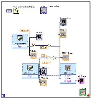
Figure 4.6: LabviewTM Block Diagram Used to Test the EIS Sensors ... 39
Figure 4.7: Circuit used to Test Water in Oil Sensor... 39
viii
Figure 4.9: Diode Output Voltage vs. Temperature ... 42
Figure 4.10: Temperature Test Circuit... 43
Figure 4.11: LabviewTM Block Diagram used to Test the Temperature Sensor... 44
Figure 5.1: Test Bench Used... 46
Figure 5.2: Labview Control Panel for Design 1... 46
Figure 5.3: Bode Plot Labview Control Panel for Design 1 ... 47
Figure 5.4: Bode Plot of Virign and Used Briggs Racing Oil ... 48
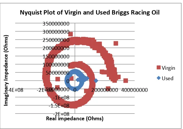
Figure 5.5: Nyquist Plots of Device 15... 49
Figure 5.6: Bode Plots of Devices 15-18 Tested by Outside Company ... 50
Figure 5.7: Nyquist Plot of Devices 15-18 Tested by Outside Company... 50
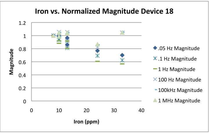
Figure 5.8: Iron vs. Magnitude Measured by Device 18 ... 52
Figure 5.9: Iron vs. Normalized Magnitude Measured by Device 18 ... 53
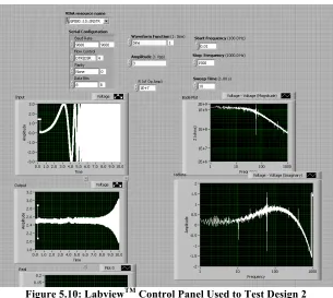
Figure 5.10: LabviewTM Control Panel Used to Test Design 2 ... 54
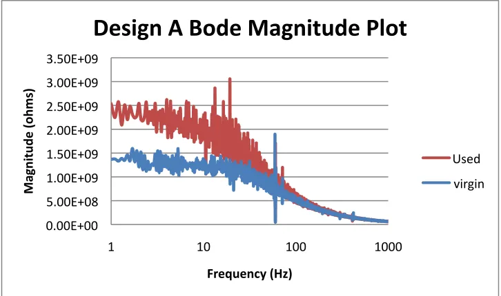
Figure 5.11: Design A Bode Magnitude Plot... 55
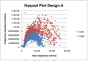
Figure 5.12: Nyquist Plot of Design A ... 56
Figure 5.13: Device 18 Water in oil Sensor... 57
Figure 5.14: Honeywell Sensor Data ... 58
Figure 5.15: Normalized Change in Capacitance of Device 18 and the Honeywell Sensor ... 59
Figure 5.16: Design A Water in oil Data ... 60
Figure 5.17: Design B Water in oil Data ... 61
Figure 5.18: Normalize Capacitance Change of Designs A and B... 62
Figure 5.19: Change in Resistance with Varying Temperatures ... 63
Figure 5.20: LabviewTM Control Panel for Temperature Testing... 64
Figure 5.21: Vout vs. Temperature of Three Different Temperature Sensors ... 65
Figure 5.22: Theoretical Change in Vout vs. Temperature with Different Temperature Coefficents ... 66
Figure 5.23:Vout vs. Temperature with Device 16-1 Tested Repeatedly ... 67
Figure 5.24: Temperature Testing Data from Outside Company ... 68
Figure 5.25: Design 2 Temperature Testing ... 70
Figure A.1: Lead vs. Magnitude Measured by Device 18 ... 75
Figure A.2: Lead vs. Normalized Magnitude Measured by Device 18 ... 75
Figure A.3: Nickel vs. Magnitude Measured by Device 18 ... 76
Figure A.4: Nickel vs. Normalized Magnitude Measured by Device 18... 76
Figure A.5: Silicon vs. Magnitude Measured by Device 18... 77
Figure A.6: Silicon vs. Normalized Magnitude Measured by Device 18... 77
Figure A.7: Soot vs. Magnitude Measured by Device 18... 78
Figure A.7: Soot vs. Normalized Magnitude Measured by Device 18... 78
Figure A.8: Design B Bode Magnitude Plot... 79
ix
List of Tables
Table 2.1: Different Values for Coefficients in Equation 2.10 [3] ... 11
Table 2.2: Water Solubility in PPM Calculated using Table 1 Values [3] ... 12
Table 3.1: Design 1 of EIS or Water in Oil Sensor ... 17
Table 3.2: Design 1 of Temperature Sensor ... 17
Table 3.3: Design 2 EIS Sensor ... 23
Table 3.4: Design 2 Water in Oil Sensor ... 24
Table 3.5: Design 2 Temperature Sensor... 24
Table 4.1: Data from the Temperature Calibration of the Diode... 41
Table 5.1: Contaminants at Different Mileages of Oil Tested... 51
Table 5.2: Shows the slopes of Device 16-1... 67
Table A.1: Process Flow used for Design 2... 74
1
Chapter 1: Introduction and Background
During a lubricant’s lifetime, a lubricant undergoes substantial chemical changes
due to a variety of degradation mechanisms: oxidative high temperature degradation;
contaminants by water glycol, fuel, soot, and wear metals [1]. It is difficult to predict
when degradation will occur or a contaminant will be introduced to the system. Oil
quality sensors need to be placed in the oil to check and be able to detect contaminants as
well as degradation in the oil. Current methods used to determine oil quality, routinely
performed by major engine and lubricant manufacturers, are frequent, repetitive and time
consuming [1]. In order to make a low cost on-line oil quality sensor electrochemical
impedance spectroscopy (EIS), water in oil and temperature sensing techniques will be
used.
1.1 EIS Background
EIS techniques can be used whenever a voltage controlled transfer of electrical
charge occurs at the interface between an electrode and an electrolyte [2]. This can be
modeled by the equivalent circuit of a resistor and capacitor in parallel, Figure 1.1. The
resistor, Re, is the resistance of the electrolyte and the capacitor, C, is the capacitance
between the electrodes and the oil. The field lines of the capacitor go through the bulk of
the oil. This allows a baseline measurement to be made when the oil is new and then a
2
Figure 1.1: Equivalent Circuit Used to Model EIS
When the electrode is first placed in oil a frequency sweep is done as a baseline
test before any contaminants or degradation occurs. A frequency sweep is done from 1
mHz to 10 MHz in [1] to demonstrate the impedance spectra or Nyquist plot of fresh and
oxidized oil. Figure 1.2 shows the difference between fresh and oxidized oil at 120oC
with an electrode spacing of 0.1 mm and 0.35 mm. The spacing of the electrode plays a
role in the Nyquist plot because the length of the field lines going through the electrolyte
changes. As the width of the spacing increases the resistance of the oil increase while the
capacitance decreases. The wider spaced electrode gives a larger response shown in [1].
It is also shown in Figure 1.2 that as the oil oxidizes the magnitude of the impedance
decreases. The impedance also changed at different temperatures, different electrode
surface areas, electrode separation distance and electrochemical potential and degree of
lubricant oxidative degradation [1]. Three different frequency ranges were used; low
frequency range of 1 mHz to 100 mHz, medium frequency range of 100 mHz to 10 Hz
and a high frequency range of 10Hz to 10MHz.
C
3
Figure 1.2: Impedance of Fresh (a) and Oxidized (b) Oil at 120oC of an electrode of .1 mm (square)
and .35mm (triangle) electrode spacing [1]
The low frequency range is affecected by the spacing between electrodes and is
measures the surface protective additives in the oil[1]. The medium frequency range is
affected by the surface of the electrodes and is driven by the charge accumulation due to
the absorption of the surface active lubricant additives[1]. The medium frequency gives
data about the additives used in the oil. The high frequency impedance is a factor
identified in the bulk of the soluton being tested[1]. The high frequency range tells how
4
Interdigitated sensor arrays and parralel plate electrodes where also tested in [1] to
see their different responses. The parallel plate electrodes were used to set a baseline for
the other sensors tested. It was concluded that both interdigitated sensor arrays and
parallel plate electrodes work to test oil quality.
Similar techniques used in [1] where used in [2] to determine the impedance of a
system and some conclusions were made. First, a large range of frequencies need to be
tested to determine the impedance of the oil. The high frequency limit gives the
electrolyte’s resistance [2]. The impedance can be plotted to see the degradation of oil in
a Nyquist plot in the complex plane. Lastly that the distance of the electrodes and
temperature play a role in the impedance plot.
1.2 Water in Oil Background
Water in oil or moisture in oil sensing has been used in transformers to make sure
that the electrical and mechanical properties do not deteriorate. It is well recognized that
water in oil has detrimental effects on trasnformer perfomance as well as other
applications where oil is used for lubrication. When the water in the oil exceeds the
solubility for that temperature, free water will form [3]. When free water forms in oil,
the oil does not act as a good lubrication any more. Water in oil testing is also good to
see if there are any leaks or gasket failures because in a closed system water should not
be introduced. Water in oil sensors have been made with a tube in tube design in [4].
5
dielectric is the oil between the inner and outter electrode, as water is added to the oil its
dielectric changes.
Figure 1.3: Tube in Tube Water in Oil Sensor [4]
Water in oil can be tested both off- and on-line. Offline water in oil testing is done by
analyzing a sample in a lab. On-line solution consist of either putting a water in oil
sensor directly into the oil or making a separate path for the oil to travel through. Figure
1.4 shows an on-line water in oil testing setup where the oil has a direct path to go
through a tube in tube sensor [5]. By having a specific track for the oil to go through
samples of the oil can be taken to see if there is any water in oil. Tube in tube solutions
are big and can be expensize to make and test the oil.
Figure 1.4: Online Oil Testing Setup [5]
Parallel plate and IDF capacitor solutions have also been made for testing water in
oil. A parallel plate capacitor with a dielectric of polyimide was tested in [5] as a water
6
is a moisture dynamic equilibrium between the polyimide film and transformer oil [5].
The relative dielectric of the polyimide changes as the water content in the oil changes
because the amount of water absorbed by the polyimide increases. The change in
capacitance was then translated through secondary circuitry to monitor the on-line water
in oil content in [5]. Another structure that measures relative humidity and uses
polyimide is an IDF capacitor.
In order to make a smaller, cost efficient humidity sensor an IDF relative
humidity sensor was made in [6]. The sensor made in [6] can be seen in Figure 1.5. The
IDF is covered with a polyimide film to increase sensitivity. Polyimide is a polymer
particularly suitable as humidity sensitive layer thanks to its full compatibility with
integrated circuit process, its great chemical stability, and its high permeability to water
[6]. After the fabrication of an IDF capacitor the polyimide can be added at the end of
the process. The polyimide layer absorbs the water which changes the dielectric of the
polyimide.
Figure 1.5: IDF Sensor Used in [6]
One disadvantage to the sensor designed in [6] is the parasitic capacitances which
appear between the interdigitated electrodes outside the polyimide film and affects the
output signal but are independent of the humidity [6]. Figure 1.6 shows the parasitic
7
parasitic capacitance needs to be reduced. Since the dielectric of silicon is roughly three
times larger than the dielectric of polyimide, the main capacitance is coming from the
substrate rather than the polyimide. This makes the substrate capacitance dominate the
capacitance of the sensor. Similar to the test done in [5] the sensor built in [6] could be
used as a water in oil sensor. The only difference would be how the capacitor is
manufactured.
Figure 1.6: Parasitic Capacitance Shown in IDF Sensor [6]
1.3 Temperature Sensor Background
Temperature is an important parameter to monitor in oil. By knowing the
temperature of oil a problem can be detected if the temperature is too high or low during
operation. Temperature also needs to be monitored for other sensors to maintain accurate
8
Chapter 2: Theory
2.1 Electrochemical Impedance Spectroscopy (EIS)
An IDF capacitor sensor was designed to test oil quality using the EIS techniques.
When the IDF is placed in the oil the system can be modeled as a capacitor and resistor in
parallel shown in Figure 1.1. The real and imaginary parts of the impedance then are
measured to see how the oil changes as contaminants are introduced. Figure 2.1 shows
the geometry of the IDF where s is the size of the spaces, w is the width of the fingers and
L is the length of the fingers
Figure 2.1: Geometry of IDF
The capacitance can be found by using Equation 2.1 [7]. Equation 2.1 takes into
consideration the number of fingers, N, s, w, and L. The dielectric of the oil is εr and the
field lines, shown in Figure 2.2, are taken into consideration by the Bessel Thompson
9
capacitance when glass is the dielectric accounts for 72% of the total capacitance and the
oil accounts for 28%.
𝐶=𝐿𝑁4𝜀0𝜀𝑟𝜋𝑛=1∞12𝑛−1𝐽𝑜22𝑛−1𝜋𝑠2𝑠+𝑤 (2.1)
Figure 2.2: Electric Field Lines between IDF
To better understand the relationship of capacitance and resistance in oil, a
parallel plate capacitor was tested in oil. A parallel plate capacitor varies both
capacitance and resistance, when in oil, by changing the area and spacing. Equation 2.2
shows the capacitance of a parallel plate capacitor.
𝐶=𝜌𝜀0𝜀𝑟𝑅 (2.2)
Equation 2.3 shows the relationship between the resistivity and resistance of the oil.
𝑅=𝜌𝑜𝑖𝑙𝑠𝐴 (2.3)
By rearranging Equations 2.2 and 2.3 to equal A, the resistivity of oil, ρoil, can be solved
for.
10
𝜌𝑜𝑖𝑙=𝑅𝐶𝑠𝜀0𝜀𝑟𝑠=𝑅𝐶𝜀0𝜀𝑟
(2.5)
From Equations 2.4 and 2.5 the resistance of the oil can be rearranged to solve the
resistance of the oil in terms of capacitance.
𝑅=𝜌𝜀0𝜀𝑟𝐶 (2.6)
This relationship between capacitance and resistance of a parallel plate capacitor in oil
holds true for IDF. By substituting the capacitance in Equation 2.1 into Equation 2.6 [1]
the resistance of the oil can be rewritten as
𝑅=𝜌𝜀0𝜀𝑟𝐿𝑁4𝜀0𝜀𝑟𝜋𝑛=1∞12𝑛−1𝐽𝑜22𝑛−1𝜋𝑠2𝑠+𝑤. [1]
(2.7)
2.2 Water in Oil
The water in oil IDF use the same theory as the EIS, but a layer of polyimide is
added on top of the IDF. The polyimide is added to increase the sensitivity to water in
the oil. Instead of only using the dielectric constant of the oil and glass the dielectric
constant of the polyimide and the dielectric constant of the water needs to be taken into
consideration. The dielectric constant of the polyimide changes as water is added to the
oil. The capacitance ratio of the capacitance, only due to the polyimide, with and without
water can be seen in Equation 2.8 [6]. For quick approximations to see how the
capacitance will change as water is absorbed Equation 2.8 can be used with the dielectric
11
absorbed by the polyimide, εpdry, . Cwet is the capacitance of the IDF when the polyimide
has absorbed water.
𝐶𝑤𝑒𝑡=𝐶𝑑𝑟𝑦𝜀𝑝𝑤𝑒𝑡𝜀𝑝𝑑𝑟𝑦
(2.8)
To calculate the dielectric of the polyimide as water is absorbed the Empirical Looyenga
formula [6], Equation 2.9, can be used to calculate εpwet. Where the γ factor is the
fractional volume of the water absorbed in the polyimide.
𝜀𝑝𝑤𝑒𝑡=𝛾𝜀𝑤𝑎𝑡𝑒𝑟13−𝜀𝑑𝑟𝑦13+𝜀𝑑𝑟𝑦133 (2.9)
The water solubility of the oil also needs to be taken into consideration. Equation
2.10 gives an expression for the saturation solubility of water in oil, rs, in ppm and
temperature, T, in oC [3]. There is some discrepancy for the coefficients A and B. Table
2.1 shows the different coefficient values from different authors. Table 2.2 shows the
data gathered by the different authors to describe the solubility of water in oil at different
temperatures.
𝑟𝑠=𝑒𝐴−𝐵𝑇 (2.10)
Coefficient Oommen Griffin Shell A 7.42 7.09 7.3 B 1670 1567 1630
Table 2.1: Different Values for Coefficients in Equation 2.10 [3]
T (oC) Oommen Griffin Shell
0 20 23 22
10 33 36 35
20 53 56 55
30 82 83 84
12
60 255 243 255 70 358 334 355 80 491 450 484 90 663 596 648 100 880 777 855
Table 2.2: Water Solubility in PPM Calculated using Table 1 Values [3]
The data in Table 2.2 was plotted in Figure 2.3. The average was taken of all of
the data and an average expression for rs was found. A new expression can now be used
to calculate rs, shown in Equation 2.11.
Figure 2.3: Water Solubility of Oil
𝑟𝑠𝑎𝑣𝑔=25.834𝑒.0363𝑇 (2.11)
yO = 24.339e0.0375x
R² = 0.992 yG = 27.136e0.035x
R² = 0.9929 yS = 26.066e0.0365x
R² = 0.993 yAVG = 25.834e0.0363x
R² = 0.9927
0 200 400 600 800 1000 1200
0 20 40 60 80 100 120
Wa
te
r S
ol
ub
ili
ty
o
f O
il
(p
pm
)
Temp (C)
Water Solubility of Oil
Oommen Griffen Shell Average
13
There is a linear relationship between the relative humidity of the oil and the moisture
content of the oil, r, shown in Equation 2.12 [3], where RH is the percent relative
humidity (%).
𝑟=𝑟𝑠𝑎𝑣𝑔𝑅𝐻100
(2.12)
2.3 Temperature Sensor Theory
The resistance of a thin film resistor can be found by knowing the resistivity, ρ,
length, L, width, w, and thickness, t, of the metal. Figure 2.4 shows the geometry of the
metal resistor. The resistance, R, can then be found by Equation 2.13.
Figure 2.4: Geometry of a Metal Resistor
𝑅
=
𝜌𝐿𝑤𝑡
(2.13)As temperature changes, the resistance of a metal resistor also changes. The
change in resistance is due to the thermal coefficient of resistance, α, is usually positive
for metals. Tantalum thought can have wither a positive or negative temperature
coefficient of resistance. Figure 2.5 shows the change in resistance of a nickel resistor
W
L
14
with temperature. The change in resistance due to α and the change in temperature, T, is
shown in Equation 2.14 [8]. RT is the new resistance at temperature, T2. The original
temperature, T1 is also needed to calculate the change in temperature. Although α has
units of ppm/oC, a change in temperature can result in a voltage change in the mV or
higher range, depending on the current.
Figure 2.5: Change in Resistance due to Temperature of a Tantalum Thin Film Resistor [8]
15
Chapter 3: Design
Two revisions of a MEMS multi sensor were designed to include EIS,
water-in-oil and temperature. A glass substrate was chosen for both revisions instead of a silicon
substrate to reduce parasitic capacitance, as seen in [6]. The advantage to a glass
substrate is the EIS and water in oil sensors are more sensitive to changes in the oil
because glass has a lower dielectric constant than silicon. The dielectric constant of glass
is 3.9 and the dielectric of oil is roughly 1.5, depending on the oil. This means that the
oil contributes to 28% of the capacitance. If silicon was used as the substrate the oil
would only contributes to 11% of the capacitance since silicon’s dielectric constant is
11.7 and the oil would only account for 11% of the change in capacitance. A glass
substrate will allow the EIS and water-in-oil to be more sensitive to contaminants,
degradation of the oil and water in oil.
3.1 Design 1
The die size for Design 1 was 5mm x 5mm, which allowed eighteen different
designs to fit on one mask. There were eighteen different IDF designs and one
temperature sensor designed. A full factorial design of experiments was done by
changing the w and s of the IDF and keeping L constant, Table 3.1. N was designed to be
the maximum number of w and s that fit with in the area given and was the overall length
l divided by L. The size of the w and s were designed to be 5µm, 12.5µm or 20µm, which
16
capacitance was constrained by the dimensions of the chip, a larger area would allow for
higher capacitances. The IDF were designed to be used for either EIS or water in oil
sensors depending on the size of w and s. The smaller w and s were designed to be the
water in oil sensors because they would have a larger change in capacitance resulting
from water added to the oil. The larger w and s were designed to be EIS sensors. But all
of the IDF designs can be used for either EIS or water in oil sensors. The only difference
is that to detect water in oil, the IDF are coated with a thin layer of polyimide. The thin
film resistor was designed to be 6kΩ on all chips. Table 3.2 shows the design of the
temperature sensor. The layout for Design 1 sensors is shown in Figure 3.1. Each chip
has one temperature sensor and one set of IDF. All of the sensors were designed to be
tantalum because tantalum does not corrode in oil and the same processing steps could be
used for all sensors.
Device s (um) w (um) l (m) L (um) N Cglass (pF) Coil (pF) C (pF)
1 5 5 0.75 4390 157 23.44 9.01 32.45
2 5 5 1 4390 209 31.25 12.02 43.27
3 5 12.5 0.5 4375 105 21.49 8.27 29.76
4 5 12.5 1.27 4375 241 49.47 19.03 68.49
5 5 20 0.5 4360 105 24.99 9.61 34.60
6 5 20 0.75 4360 158 37.48 14.41 51.89
7 12.5 5 0.5 4390 104 11.37 4.37 15.74
8 12.5 5 0.75 4390 157 17.06 6.56 23.62
9 12.5 12.5 0.3 4375 63 9.37 3.60 12.98
10 12.5 12.5 0.6 4375 126 18.74 7.21 25.95
11 12.5 20 0.45 4360 95 16.60 6.38 22.98
12 12.5 20 0.65 4360 129 22.65 8.71 31.36
13 20 5 0.35 4390 73 6.85 2.64 9.49
14 20 5 0.5 4390 104 9.79 3.77 13.56
15 20 12.5 0.35 4375 73 9.27 3.56 12.83
16 20 12.5 0.6 4375 122 15.42 5.93 21.35
17
18 20 20 0.5 4360 99 14.72 5.66 20.38
Table 3.1: Design 1 of EIS or Water in Oil Sensor
Temp s (um)
w (um)
t
(um) N rho (uΩ/cm) l
(um) L (um) R (Ω)
1 10 20 0.4 10 120 3800 38100 5720
Table 3.2: Design 1 of Temperature Sensor
Figure 3.1: Layout for Design 1 Multi Sensor
3.2 Fabrication of Design 1 Multi Sensor
Design 1 of the multi sensor was fabricated at R.I.T. during the summer of 2011.
Fabrication began with a 6 inch glass wafer. Figure 3.2 shows the cross sectional view of
the glass wafer before fabrication.
Figure 3.2: Cross Section of Wafer before Fabrication
The first step was to deposit tantalum (Ta) onto the wafer using the CVC 601.
The wafers are first loaded into the CVC 601 and the chamber is pumped down until the Glass Substrate
EIS or water in oil Sensors
18
base pressure is below 1x10⁻⁵Torr. A pre-sputter was done for 5 minutes with a radiant
heat at 200oC. Then a 2 minute sputter of TaN (9% N2) was done with power at 175
watts, 5mTorr of Ar and .5mTorr N2. This was immediately followed by a Ta sputter
with a power of 200 watts, 5.5mTorr of Ar for 30 minutes. Figure 3.3 shows the cross
sectional view after depositing Ta. The resulting Ta was 2500Ǻ thick and was alpha-Ta.
Beta-Ta was also fabricated using a higher power of 500watts.
Figure 3.3: Cross Section of Wafer after depositing Ta
The problem with getting a different Ta is they have different temperature
coefficients and the signal processing needs to account for whether or not the change in
resistance will change the voltage either positively or negatively. Alpha-Ta has a positive
temperature coefficient where beta-Ta has a negative temperature coefficient. It was
believed that the variation in thickness would only have an effect on the difference in
resistance and not have an affect on the temperature coefficient (see section Testing
Temperature Sensor Design 1 for more details).
Following the Ta sputter, the wafer was then coated with photoresist on the SSI
track one using coat.rcp. Coat.rcp is a three step process which starts which a dehydrate
bake at 140oC with a HMDS vapor prime for 60 seconds. The wafer is then spin coated
with OIR 620-10 resist at 3250 rpm for 30 seconds followed by a soft bake at 90oC for 60
19
Figure 3.4: Cross Section After wafer is coated with Photoresist
The photoresist was then exposed using the ASML Stepper with an exposure dose
of 250mJ/cm2; see Figure 3.5 for the mask design. The photoresist was then developed
using the SSI Track 2 using develop.rcp. Develop.rcp begins with a post exposure bake
of 110oC for 60 seconds. The exposure bake is followed by developing the resist with
CD-26 developer for 50 seconds, a rinse of DI water for 30 seconds and a spin dry for 30
seconds at 3750 rpm. The last step of developing the photoresist is a Hard Bake at 140oC
for 60 seconds. Figure 3.6 shows the cross sectional view of the wafer after the
photoresist is exposed and developed.
Figure 3.5: Mask Layout of Design 1 Multi Sensor
20
Figure 3.6: Cross Section After Develop
After the photoresist was developed the Ta was then plasma etched using the
LAM 490. Recipe FNIT1500 was used to etch the Ta in three steps. The first step’s
chamber pressure is 260mTorr, a gap of 1.65cm, no power and 200sccm of SF6 for 1
minute. The second step has the same parameter used in step 1, but the power is turned
onto 125watts and there is endpoint detection or a max time of 30s. The last step’s
chamber pressure is 260mTorr, a gap of 1.65cm, 125 watts power and 200sccm of SF6 for
a 40% over etch. Figure 3.7 shows the cross sectional view after the plasma etch.
Figure 3.7: Cross Section after Plasma Etch
The last step of fabrication is to strip the photoresist in acetone, rinse in DI water
and then spin rinse dry. The final cross sectional view is shown in Figure 3.8. Upon
completion of fabrication the wafer was inspected under a microscope to make sure there
are not unwanted opens or shorts on the devices. Figure 3.9 shows the wafer after
21
Figure 3.8: Final Cross Section of Device
Figure 3.9: Wafer After
After fabrication the devices were cut using the wafer saw and the capacitance
and resistance were checked. Some of the chips were hand painted with polyimide to
turn the IDF into water in oil sensors.
Device #5 and #10 had shorts from manufacturing defects from the mask, so none
of those chips worked. The devices with s=5µm had shorts on all the devices. This may
be because the fingers were to close together that a small particle can short the device
from the wafer saw or from some unknown factor. Only a couple of devices with
s=12.5µm worked, but the majority had similar problems as with s=5µm and would be
hard to consistently manufacture following this process. The majority of the devices with
s=20µm worked. Figure 3.10 shows a manufactured multi sensor with w=20µm and Glass Substrate
22
s=20µm. In order to consistently get smaller w and s a new process would need to be
made.
Figure 3.10: Manufactured Multi Sensor
3.3 Design 2
A redesign was needed after testing Design 1. Design 2 needed to address the
following improvements; all sensors need to be on one chip, increase the nominal value
of the capacitance of the water in oil sensor, be able to solder to the chip and fix the
crystal structure problem of Ta. All three sensors where integrated onto one 6.5mm x
6.5mm chip, Figure 3.11 shows the chip layout. This was accomplished by designing
23
Figure 3.11: Design 2 Chip Layout
The EIS sensor has similar w and s as Design 1. Two EIS sensor combinations
were designed with different w and s because 20µm worked well in Design 1. An IDF
with 15µm w and s was designed to give a larger capacitance. The EIS sensor was made
with two different L. The first L was made to fit between the EIS pads, the same as in
Design 1, but the second L was designed to fit inside the pads of the temperature sensor.
The second L is smaller than the first because it had to spaced away from the temperature
sensor’s pads to avoid making electrical shorts. The total capacitance is the capacitance
from the two different Ls added together in parallel. This was done to optimize the
length of the chip. Table 3.3 shows the EIS designs.
EIS s (um) w (um) l1 (um) l2
(um) N1 N2
Cglass1 (pF) Cglass2 (pF) Cglass Total (pF) Coil (pF) Ctotal (pF)
A 15 15 3970 3970 67 57 9.02 7.67 16.70 4.64 21.33
B 20 20 3960 3960 50 43 6.75 5.74 12.49 3.47 15.96
Table 3.3: Design 2 EIS Sensor
Temperature Sensor
24
The water in oil sensor needed a larger nominal capacitance. This was achieved
by decreaseing the size of the w and s to either 2 or 3µm and increasing N. Table 3.4
shows the two different water in oil designs. By increasing the nominal capacitance the
change in capacitance will increase and will be easier to measure.
Water in Oil s (um) w (um) l1 (um) l2
(um) N
Cglass (pF) Cpolyimid (pF) Ctotal (pF)
A 2 2 3996 3996 500 68.13 26.20 94.33
B 3 3 3994 3994 333 45.40 17.46 62.86
Table 3.4: Design 2 Water in Oil Sensor
Soldering to the pads instead of wiring bonding became a priority for packaging,
so the metal was changed from Ta to a Titanium/Nickel (Ti/Ni). Originally a layer of Ni
was going to be sputtered ontop of the Ta, but Ni can not be plasma etched. The Ta
crystal problem would also still not be resolved. Another problem with plasma etching is
it does not consistantly etch the small w and s. So by decreasing the size of w and s for
the water in oil sensor a new manufacturing process is needed. Switching the metal to
Ti/Ni also solved the alpha/beta crystal structure problem that gives two different thermal
coefficients of resist, one positive and the other negative. By changing the metal, the
temperature sensor became easier to manufacture reliably. The overall resistance of the
temperature sensor was also increased to achieve a bigger change in voltage with
temperature change. Table 3.5 shows the design of the temperature sensor. There were
four different combinations designed in Design 2. All combinations for the EIS sensor
and water in oild sensor were manufactured with the temperature sensor.
Temp s (um) w (um) t (um) N rho (uΩ/cm) l (um) L (um) R (Ω)
1 5 5 0.15 20 9.5 4190 83900 10627
25
3.4 Fabrication of Design 2 Multi Sensor
The process to manufacture Design 2 had to be changed because of the smaller w
and s of the water in oil sensor and using a different metal, Ti/Ni. Both the smaller w and
s was too difficult to with RIT’s processing capacbilities. By changing the feature size
and the metal a new process was used to manufacture Design 2 that utilizes a negative
photoresist, evaporation and lift-off.
Design 2 of the multi sensor was fabricated at R.I.T. during the winter of
2011-2012. Fabrication began with a 6 inch glass wafer, see Figure 3.3. The first step of
processing was a piranha clean. The piranha clean is used to remove organic materials
that could have formed on the glass substrate. A piranha clean is a 1:1 solution of
Sulfuric Acid (H2SO4) and Hydrogen Peroxide (H2O2) that is heated to 130oC. The wafer
is then placed in the solution for 15 minutes. The piranha clean is followed a DI rinse for
5 minutes and a spin, rinse, dry. Once the wafer is dry the wafer is ashed using the
GaSonics Asher. An oxygen plasma etch was done for 198 seconds using Recipe FF on
the GaSonics Asher. After being ashed the wafer is ready to be coated with photoresist.
The wafer was coated using SSI Track 1 recipe NLOFCOTG. First the wafer
underwent a dehydration bake with HMDS Vapor prime at 140oC for 3 minutes and was
followed by a 30 second cool. AZ nLOF 2020 negative photoresist was then hand coated
on the wafer at 2500 rpm for 60 seconds. A soft bake at 110oC for 3 minutes followed.
26
Figure 3.12: Cross Sectional View after Coating with Photoresist
The photoresist was then exposed using the ASML Stepper with an exposure dose
of 66mJ/cm2; see Figure 3.13 for the mask used. The mask had two defects on it; one
was a short one of the EIS sensors and water in oil sensors. The photoresist was then
developed using the SSI Track 2 using DEVNLOFG.rcp. DEVNLOFG.rcp begins with
an Image Reversal Bake of 110oC for 3 minutes followed by a 30 second cool. Then the
photoresist is developed with CD-26 developer for 5 seconds while spinning at 50rpm.
Then more CD-26 is dispensed for 5 seconds and the photoresist is developed for 70
seconds. After the developer a rinse of DI water is done for 30 seconds at 1000rpm. This
is followed by a spin dry for 30 seconds at 3750 rpm. Figure 3.14 shows the cross
sectional view of the wafer after the AZ nLOF 2020 is exposed and developed.
Figure 3.13: Mask Used for Design 2
27
Figure 3.14: Cross Sectional View of Design 2 after Develop
Once the photoresist is developed the wafer is ready for evaporation. Evaporation
of the Ti/Ni was chosen over sputtering because the lift-off was difficult to do and the
small features had shorts or were gone altogether. One advantage of sputtering is it can
hide changes in height. This means that when the Ti/Ni was sputtered on to photoresist
there was not a gap between the metal on top of the photoresist and the metal on the
substrate, making it difficult to off. Figure 3.15 shows IDF after an unsuccessful
lift-off with sputtered Ti/Ni. Notice that not all the spaces are cleared thus shorting the two
electrodes.
Figure 3.15: Unsuccessful Lift of Ti/Ni that was Sputtered
The CVC evaporator was used to evaporate the Ti and Ni onto the wafer. The Ti
acts as an adhesion layer between the glass and the Ni. Before evaporation, one pellet of
Ti, .110 grams, was placed in a woven tungsten (W) basket and placed into the CVC
28
thickness of the deposited Ti to be ~300Ǻ. The CVC evaporator will allow up to four
different metals to be evaporated during one run of the machine. Two pellets of Ni, .218
grams each, are placed into separate woven W baskets and are put in the next available
position in the CVC evaporator. One pellet of Ni gives a thickness of ~300Ǻ at 25cm
away from the W basket. After the Ti is deposited the operator must move the first Ni
pellet into position to be evaporated and move the second Ni pellet into position after the
first Ni pellet is evaporated.
Once the W baskets are loaded with the correct metal, the bell jar of CVC
evaporator needs to be closed and the chamber will begin to pump down. Before
evaporating the Ti, the chamber needs to be pumped down to 2x10⁻⁶Torr. The Ti can
then be evaporated by turning on the filament and slowly increasing the power to
220-240V. The Ti will begin to evaporate around 220V. The power was kept between 220V
and 240V until the Ti was completely evaporated. Figure 3.16 shows the cross sectional
view of after the Ti was evaporated.
Figure 3.16: Cross Section of Design 2 after Ti Evaporation
After the Ti was fully evaporated the first Ni pellet is moved into position to be
evaporated. After the chamber has pumped back down to 2x10⁻⁶Torr the Ni can be
evaporated. The filament was ignited and the power was slowly increased to 200V.
Around 200V the Ni begins to evaporate. The power was kept between 200V and 220V
29
until the Ni was completely evaporated. The second pellet of Ni is evaporated the same
way as the first after the chamber has pumped down again. Figure 3.17 shows the cross
sectional view wafer after both Ni pellets are evaporated. The two pellets are evaporated
separately because when evaporated at the same time, not all of the Ni is evaporated. The
Ni does not fully evaporate because the W basket usually breaks before the evaporation is
complete. The pressure in the chamber also increases because the evaporation takes a
longer amount of time and more power than evaporating the pellets separately.
Figure 3.17: Cross Section of Design 2 after Ni is Evaporated
The last process step for fabricating Design 2 was to remove the photoresist and
unwanted metal through lift-off. Lift-off was done using the Ultrasonic Wet Bench.
A square glass dish was placed with the bottom of the dish in the DI water of the
Ultrasonic Wet Bench. Half an inch of acetone was poured into the glass dish. The
ultrasonic was turned on and the wafer was placed in the acetone. While the Ti/Ni is
being lifted off a magnet was used to pick up all loose metal. The lift-off takes a couple
of minutes. After all the unwanted metal is lifted-off the wafer was rinsed in DI water.
Figure 3.18 shows the cross sectional view wafer after lift-off.
Figure 3.18: Cross Section of Design 2 after Lift-Off
30
The wafer was inspected under a microscope to make sure that the lift-off was
complete. Figure 3.19 shows a section of all three finished sensors water in oil sensor.
Visually, most of the sensors looked good. The wafer was cut using the wafer saw before
being tested. Polyimide was painted on to the water in oil sensor.
31
Chapter 4: Packaging and Test Setup
In order to test the sensors, packaging, testing procedures and signal conditioning
was created to test each sensor. After the wafers were diced each chip needed to be
packaged before being able to be tested. In order to test each sensor, three separate tests
were created with their own circuitry. LabviewTM was used to test the EIS and
Temperature sensors, while an Arduino was used to test the Water in Oil sensor. Each
test had its own signal conditioning and procedure for testing. Each circuit was then
placed onto a single PCB, shown in Figure 4.1, for final testing.
Figure 4.1: Final PCB for Signal Processing
4.1 Packaging
Before packaging any chips, they were checked under the microscope and probed
with fine tipped wafer probes. They were then connected LCR meter to check for opens
and shorts. The LCR meter showed whether or not the EIS or water in oil sensor had
32
sensor. For the capacitance sensors, the phase needs to close to -90 degrees. This
ensures that the device is purely a capacitor. Some devices had both a capacitance and
resistance. These devices were not packaged because the sensor will not work as
designed. Occasionally a device will have a phase of 90 degrees and have a short circuit,
but will show up on the LCR meter as an open. To double check that there is not any
resistance, resistance is measured using a multi-meter. The multi-meter should read
overload, which indicate that there is an open. When checking the capacitance sensors
the resistance must be zero for them to function properly. If the resistance was not zero
then that device was not packaged. The temperature sensor was also checked using the
LCR meter, but since it is resistor the LCR meter measured the resistance and made sure
there was not an open. The impedance was also measured and the phase was 90 degrees.
After each sensor on a chip was checked using the LCR meter the water in oil sensor
needed have polyimide painted onto the IDF.
Before coating the polyimide, the chip was cleaned with acetone and isopropyl
alcohol. The polyimide used was HD Microsystems PI-2556 and is painted onto the water
in oil sensors’ IDF. The polyimide is applied by taking a wire and dipping it into the
polyimide so a drop of polyimide is on the tip of the wire. The polyimide is then applied
on the IDF until all the fingers are covered. IT is important not to cover the pads with
polyimide because it is difficult to wire bond through polyimide. If one drop did not
cover the entire fingers a second drop should be applied carefully not to cover the other
sensors. Once the polyimide has been applied it needs to be cured in the oven for 30
33
PCB because the epoxy will melt at 200oC. Figure 4.2 show a chip from Design 1 and
Design 2 after the polyimide has been applied. After the polyimide has been cured the
chip or chips, Design 1, are ready to be packaged.
Figure 4.2: Polyimide applied to Design 1 (Left) and Design 2 (Right)
Copper PCBs were designed using expressPCB software and were manufactured
at RIT. A different PCB was designed for each sensor because of the different sizes and
pad placement. Design 1 needed two chips to be placed on one PCB to be able to
measure EIS, water in oil, and temperature since each chip sensed EIS or water in oil.
Since design 2 incorporates all sensors on one chip, only one chip is needed. The chips
were epoxied to the PCB and wire bonds were used to connect the pads to the PCB.
Epoxy was then used to cover the wire bonds, to prevent them from breaking during use
34
Figure 4.3: Packaged Design 1(Left) and Design 2 (Right)
The pin out for both designs is exactly the same so the same cables can be used to
test both devices. The outside pins are for water in oil, the second pins in from each side
is the temperature sensor and the middle two pins are for EIS. As long as the correct pins
are hooked up it does not matter which pin is in or out, they are interchangeable.
4.2 EIS Test Setup
In order to test oil quality using the EIS sensor, frequency analysis and the
impedance of the EIS sensor in parallel with the resistance of the oil needs to be
measured. A LabviewTM routine was created to test the sensors. Before testing the
devices the signal conditioning circuit for EIS Testing, Figure 4.4, was simulated in
MATLAB. The transfer function of the signal conditioning circuit was found by first
35
Figure 4.4: Signal Conditioning Circuit for EIS Testing
𝑍𝐶𝐸𝐼𝑆=1𝑠𝐶𝐸𝐼𝑆
(4.1)
This was then combined in parallel with the resistance of the oil, Equation 4.2, to find the
impedance at the input of the op-amp, Z1.
𝑍1=𝑅𝑜𝑖𝑙||𝐶𝐸𝐼𝑆=1𝑅𝑜𝑖𝑙+𝑠𝐶𝐸𝐼𝑆−1=𝑅𝑜𝑖𝑙1+𝑠𝐶𝐸𝐼𝑆𝑅𝑜𝑖𝑙
(4.2)
The impedance of the output, Z2, is just the resistor R2is shown in Equation 4.3. R2 was
chose to be 1MΩ to magnify voltage change at V1.
𝑍2=𝑅2 (4.3)
The transfer function is then found by dividing the impedance of the output by the
impedance of the input times negative one to account for the inverting amplifier. Z1
36
Equation 4.4 shows the transfer function of the signal conditioning circuit used for EIS
Testing.
𝐻𝑠=−𝑍2𝑍1=−𝑅2𝑅𝑜𝑖𝑙1+𝑠𝐶𝐸𝐼𝑆𝑅𝑜𝑖𝑙=−𝑅2𝑅𝑜𝑖𝑙1+𝑠𝐶𝐸𝐼𝑆𝑅𝑜𝑖𝑙
(4.4)
The transfer function in Equation 4.4 was simulated using MATLAB to better understand
what the output of the EIS testing would be when a frequency sweep was done at the
input, V. Figure 4.5 shows the bode plot simulated in MATLAB. The bode plots of the
EIS signal conditioning circuit has one pole when modeled by capacitor and resistor in
series. The magnitude continues to increase after the pole. The simulated bode plot was
done with the CEIS=90pF and Roil=20MΩ. The phase is dominated by the capacitance of
the EIS sensor and there is a 90 degree change beginning a decade before the pole at 555
rad/s and continues until a decade after the pole.
37
Although knowing the output of the circuit is important the change of impedance
at node V1 of Figure 4.1 is what we are looking for to see the change in oil quality. Since
impedance, by itself, cannot be measured using LabviewTM, nodal analysis was done to
find what the impedance is at node V1 by knowing the input and output voltages.
The voltage at the input and output can easily be measured. By using nodal
analysis at node V1, the magnitude of impedance can be found. Since impedance is the
voltage divided by the current and no current goes through the op-amp, the current
through Z1 must be the same as the current through Z2. The impedance of the EIS sensor
and Roil can then be calculated by using Equation 4.5. 2.5V was subtracted from Vout to
get rid of the DC voltage of the single power supply.
𝑍𝑚𝑎𝑔𝑉1=−𝑉𝑖𝑛𝐼=𝑉𝑖𝑛𝑉𝑜𝑢𝑡−2.5𝑉𝑅2=−𝑉𝑖𝑛𝑉𝑜𝑢𝑡−2.5𝑉𝑅2
(4.5)
The phase was found by using a Fast Fourier Transform in LabviewTM. The phase along
with the magnitude of the impedance can be used to find the real and imaginary parts of
the impedance, shown in Equations 4.6 and 4.7. After obtaining the real and imaginary
parts of the impedance a Nyquist plot can be used to compare new and used oils. In order
test the EIS sensors LabviewTM was used to control the signal generator, measure the
input and output voltages, and do frequency analysis.
𝑍𝑟𝑒𝑎𝑙=𝑍𝑚𝑎𝑔𝑉1cos𝜑 (4.6)
38
Then a LabviewTM routine began by controlling the Agilent 33220A Waveform
Generator. A sine wave with a magnitude of 3V peak to peak was logarithmically swept
for 10 seconds from .01Hz to 1500Hz. Only frequencies in the range of 1 Hz to 1k Hz
were analyzed. It was found that by starting and ending out of the frequency range of
interest the noise of the signal was greatly reduced. Two National Instruments (NI)
USB-6008s were used to measure the input signal of the waveform generator and the output
signal of the EIS signal conditioning circuit, Figure 4.1. Both NI devices were set to N
Samples, with a sample rate of 10 kHz and the number of sample was set to 100,000 or
10 seconds at a rate of 10 kHz. The input and the output where then compared using a
Dual Channel Spectral Measurement Block (DCSMB). This gave the magnitude and the
phase of the EIS signal conditioning circuit at the output. In order to get the impedance
at node V1 Equation 4.5 needed to be found. This was accomplished by inverting the
output signal, subtracting 2.5 Volts and then dividing by R2 before comparing the input
and the output signals in a DCSMB. The magnitude, real, and imaginary parts of the
impedance was taken directly taken from a DCSMB. The phase was then calculated by
taking the arctangent of the imaginary part divided by the real part of the impedance,
shown in Equation 4.8. The LabviewTM Block diagram used is shown in Figure 4.6.
39
Figure 4.6: LabviewTM Block Diagram Used to Test the EIS Sensors
4.3 Water in Oil Test Set Up
Testing of the water in oil sensor was conducted using an Arduino. The Arduino
supplied the power, ground and was programmed to find the change in capacitance. The
signal conditioning for water in oil testing consisted of an oscillating circuit. Figure 4.7
shows the oscillator circuit used to test the water in oil sensor. The oscillator circuit
outputs a square wave whose period changes as the capacitance of the water in oil sensor
changes.
40
The Arduino counts the number of pulses for 1 second and calculates the period,
T, using Equation 4.9. Equation 4.9 can be re-arranged to find the capacitance of the
water in oil sensor (CWIO), shown in Equation 4.10. The Arduino code was written by
Dan Smith.
𝑇=2ln3𝑅𝐶𝑊𝐼𝑂 (4.9)
𝐶𝑊𝐼𝑂=𝑇2ln3𝑅
(4.10)
To test for water in oil, the Water in Oil sensor was submerged in 400 mL of
virgin oil. The oil was then heated to 50o C on a hot plate to eliminate temperature as a
variable. The hotplate temperature was set to 60o C to keep the oil at 50oC. In order to
mix the water and oil a spinner was placed at the bottom of the oil and spun during the
entire test at 1500 rpm. The oil was left alone for 10 minutes to get a baseline and then .3
mL or 750 ppm of water was added every 10 minutes until there was 3 mL or 7500 ppm
of water in the oil.
4.4 Temperature Test Set-up
LabviewTM and the NI USB-6008s were again used to test the temperature sensor.
In order to characterize and test the temperature sensor, they were tested in an oven while
increasing and decreasing the temperature. Since the voltage of a diode changes by
-2.2mV/oC, a diode was used to calibrate the temperature sensor. A diode was used
41
with LabviewTM, making it easy to compare the change of temperature sensor to the
diode and automate the testing. LabviewTM was used to measure the output voltage of the
diode every 5 oC from 35 to 100oC. Figure 4.8 shows the circuit used to measure the
voltage change of the diode. Table 4.1 shows the data collected from the temperature
calibration.
Figure 4.8: Diode Circuit used to Calibrate Temperature Sensor
Temperature (oC) Vout (V)
35 0.422
40 0.392
45 0.38
50 0.372
55 0.364
60 0.351
65 0.339
70 0.324
75 0.311
80 0.3
85 0.287
90 0.273
95 0.263
100 0.252
42
From this data a linear relationship was found between the output voltage of the diode
and the temperature of the oven. Figure 4.9 shows the Diode Output Voltage vs.
Temperature. The equation found from the best fit was, T = -400.59(Vdiode) +199.98,
was then programmed in LabviewTM to change the voltage measured of the diode into
temperature.
Figure 4.9: Diode Output Voltage vs. Temperature
After calibrating the diode so temperature could be easily captured using
LabviewTM the temperature sensor was ready to be tested. A half Wheatstone bridge was
used with a matching resistor to set the output voltage at .3 V at room temperature for
Design 1. It was difficult to consistently match the reference resistor to the temperature
sensor because of variations in the thickness of the resistor. Also, since the nominal
resistance was increased by ten times in Design 2 and for better repeatability, a
potentiometer, which ranged from 1 to 100kΩ, replaced the reference resistor and the
T = -‐400.59(Vdiode) + 199.98 R² = 0.9935
0 20 40 60 80 100 120
0.2 0.25 0.3 0.35 0.4 0.45
Te
m
pe
ra
tu
re
(C
)
Diode Output Voltage (V)
Diode Output Voltage vs. Temperature
43
output voltage was set to .5 volts. The circuit used to measure the temperature sensor is
shown in Figure 4.10. As temperature increase the resistance of the temperature sensor
increases, this changes the voltage of the half Wheatstone bridge at node V1. The
voltage of the half Wheatstone bridge was then amplified by a non-inverting amplifier
and recorded at the output. The gain of the non-inverting amplifier was 11V/V. The
output voltage was then measured using the NI USB-6008 and the temperature was then
found using LabviewTM.
Figure 4.10: Temperature Test Circuit
Each sensor was placed in the oven with the diode at room temperature (24oC)
before the oven was turned on. The oven was then heated to 100oC and turned off. The
oven was then left to cool back to room temperature with the door closed. Opening the
door makes the diode cool faster than the temperature sensor. But if diode and
temperature sensor are both placed in oil, the door can be opened so the oil cools quicker,
this allowed for both the diode and temperature sensor to cool at similar rates. The
output voltages of the diode and temperature test circuit were both measured using
LabviewTM and then exported to excel to be analyzed. The LabviewTM block diagram
44
45
Chapter 5: Testing Results and Discussion
After individual chips were packaged the individual sensors were tested using the
processes described in Chapter 4. Designs 1 and 2 were both tested at RIT. Design 1’s
EIS and temperature sensors were also tested by an outside company in the Fall of 2011.
Design 2 will be tested by the same company at a later date. The test bench used can be
seen in Figure 5.1. The test bench was able to test all devices. Beakers of clean and dirty
oil were used for EIS and water in oil testing. A hotplate was used to keep the
temperature constant during water in oil testing. The oven was used to test the
temperature sensor. The Arduino was used for the single supply power source for all
signal conditioning circuits as well as measuring the water in oil. The NI USB-6008
devices were used to capture the output voltages of the EIS and temperature outputs. A
46
Figure 5.1: Test Bench Used
5.1 EIS Test Results
5.1.1 Design 1 Testing at RIT
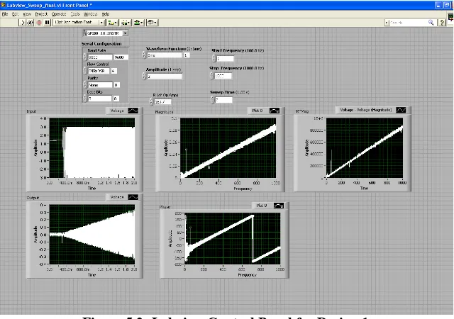
In order to test the EIS sensors a linear frequency was swept from 5 to 1000 Hz,
instead of a log sweep, and both the input and output signals were captured. Figure 5.2
shows the LabviewTM control panel used for testing Design 1. The EIS sensor on Chips
1-14 of Design 1 did not work very well. Majority of the EIS sensors were shorted
together because the lines and spaces less than 20µm were not able to be fully etched.
The fabrication process was then changed to account for this issue so smaller lines and
spaces could be made for Design 2. Devices 15-18 worked pretty well as oil quality
[image:56.612.165.485.404.629.2]sensors.
Figure 5.2: Labview Control Panel for Design 1
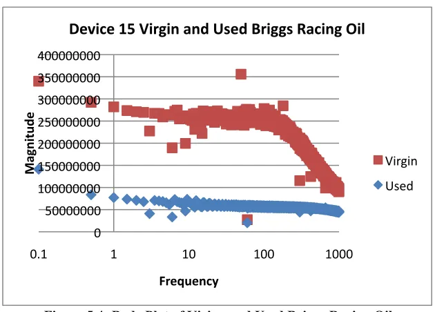
In order to asses their functionalilty, Devices 15-18 were tested in the same oil to
47
one dirty oil. The virgin oils used were Briggs Racing Oil, Royal Purple Transmission
Oil, Mobil 5W-30 engine oil. The dirty oil was Briggs Racing Oil. It was imprtant to
have a clean and dirty sample of the same oil to see the difference in impedance. Figure
5.3 shows a Bode Magnitude Plot for the response of Device 18 in Mobile 5W-30 Engine
Oil. As the frequency increases the magnitude descreases. This is what was expected to
happen with a resistor and capacitor in parallel. This is true because as low
![Figure 1.2: Impedance of Fresh (a) and Oxidized (b) Oil at 120 oC of an electrode of .1 mm (square) and .35mm (triangle) electrode spacing [1]](https://thumb-us.123doks.com/thumbv2/123dok_us/110664.10387/13.612.145.505.119.430/figure-impedance-fresh-oxidized-electrode-triangle-electrode-spacing.webp)