Int. J. Electrochem. Sci., 12 (2017) 10511 – 10523, doi: 10.20964/2017.11.38
International Journal of
ELECTROCHEMICAL
SCIENCE
www.electrochemsci.orgA Rapid, Label-free and Impedimetric DNA Sensor Based on
PNA-modified Nanoporous Gold Electrode
Wenyan Tao1,2, Peng Lin1,*, Hong Liu1, Shanming Ke1 and Xierong Zeng1 1
Shenzhen Key Laboratory of Special Functional Materials & Shenzhen Engineering Laboratory for Advance Technology of Ceramics, College of Materials Science and Engineering, Shenzhen University, Shenzhen, China
2
Key Laboratory of Optoelectronic Devices and Systems of Ministry of Education and Guangdong Pro vince, College of Optoelectronic Engineering, Shenzhen University, Shenzhen, China
*
E-mail: [email protected]
Received: 21 July 2017 / Accepted: 1 September 2017 / Published: 12 October 2017
A gold nanoparticle film was successfully prepared on highly ordered and porous anodic aluminum oxide substrate through thermal evaporation deposition technique. As-fabricated nanoporous gold electrode modified by thiol-derivative peptide nucleic acid (PNA) was applied for impedimetric DNA sensing. In-situ kinetic analysis of PNA/DNA hybridization process was realized by electrochemical impedance spectroscopy (EIS) method. Considering the special structure of nanoporous gold electrode, a new equivalent circuit model was proposed for EIS data fitting. The sensitivity of PNA-modified nanoporous gold electrode is 0.4 /cm2nM. Meanwhile, complementary DNA target could be detected at concentration as low as 10 nM, which indicating that a methodology for rapid, sensitive and label-free detection of DNA has been set-up based on nanoporous gold electrode.
Keywords: anodic aluminum oxide; nanoporous gold electrode; peptide nucleic acid; DNA sensing
1. INTRODUCTION
For example, a label-free colorimetric method was presented for simple and convenient assay of DNA methylation using unmodified Au nanorods with enzyme-linkage reaction [6]. In this method, DNA methylation and MTase activity can be readily monitored by the color change of Au nanorods.
Peptide nucleic acid (PNA) is an achiral and uncharged DNA mimic where the sugar-phosphate backbone has been replaced with a peptide like N-(2-aminoethyl) glycine polyamide structure, to which the nucleobases are connected by methylenecarbonyl linkages (Scheme 1).
'5 O
O
B a s e
O
P O
O
N a O O
B a s e
O
P O
O
N a O
n O B a s e
O
3 '
D N A
N H O
N O
B a s e
N H O
N
B a s e
O
N H O
N
n
B a s e
O
N H
P N A
Scheme 1. The structure skeleton of DNA and PNA.
PNA has been paid many attentions in electrochemical [8-10] and fluorescent method for DNA sensing [11]. PNA probe possesses two main advantages over DNA probe for hybridization: firstly, no electrostatic repulsion between PNA and negatively charged DNA, which make PNA can be highly hybridized with DNA. Secondly, PNA possesses excellent stability. PNA oligomers are neither degraded by nucleases nor proteases. Finally, no enantiomeric purity issue in PNA solution occurs due to achiral structure of PNA. Specially, facilitated by the difference in surface charge between DNA probe and duplex DNA chains, electrochemical impedance spectroscopy (EIS) method has been used in DNA sensing on the gold and boron-doped diamond electrode [12,13]. The principle of impedimetric DNA sensing is based on the formation of PNA/DNA duplex at the sensing surface. Then the negatively charged interface repels the negatively charged redox indicator, which leading to an increase in charge transfer resistance or other electric elements related to the PNA/DNA duplex. Therefore, these electric elements will increase with the increase of DNA concentration.
nano-structural films fabrication [25, 26]. AAO provides a rough surface with large surface area for supporting metal nanoparticles and formed a conductive nano-structural network which facilitates measurement of electrical property changes. Until now, there is few work based on AAO template for DNA sensing. A microfluidic-channel based electrochemical DNA biosensor was constructed by using AAO substrates as the designing templates [27]. The DNA biosensor provides 10−19 M sensitivity for detecting target DNA, which through hybridizing with flow-forced filtration of target DNA solution. Such high sensitivity is attributed to the well-defined fluidic channel structure that gives high surface area for probe DNA immobilization and enables target DNA solutions to pass through its fluidic channels for rapid and efficient hybridization. However, the fabrication of microfluidic channel is complex and time-consuming.
In this work, a type of nanoporous gold electrode fabricated on AAO substrate was used as a novel electrode for DNA sensing. Using PNA as probe, a rapid, label-free and impedimetric DNA biosensor was constructed on the nanoporous gold electrode. A new equivalent circuit model was proposed and applied in data analysis.
2. EXPERIMENTAL
2.1. Chemicals and materials
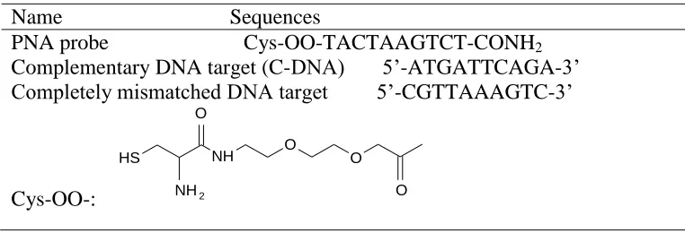
[image:3.596.107.488.533.663.2]Synthesis of PNA probe is according to the following rules: 1) the base number of PNA probe is limit in the range of 10 to18 for good affinity; 2) high purine content will cause aggregation and low solubility. It is suggested that purine content not exceeds 60%. Thiolated PNA probe was synthesized from ZIYU Biotech Co. Ltd (Shanghai, China), and target DNA were purchased from Shanghai Sangon Ltd (Shanghai, China), shown in Table 1.
Table 1. The sequences of PNA probe and DNA targets Name Sequences
PNA probe Cys-OO-TACTAAGTCT-CONH2 Complementary DNA target (C-DNA) 5’-ATGATTCAGA-3’ Completely mismatched DNA target 5’-CGTTAAAGTC-3’
Cys-OO-:
NH
O O
O
NH HS
2
O
for sample preparation was deionized on a micro-pure water purification system with resistivity of 18.2 MΩcm.
2.2 Preparation and modification of nanoporous gold electrode
Scheme 2. Schematic illustrations of PNA immobilization and PNA/DNA hybridization process on nanoporous gold electrode.
A thin gold nanoparticle film was prepared on AAO substrate by thermal evaporation deposition technique, named as nanoporous gold electrode in this work. Before film deposition, the AAO substrate were rinsed with ethanol and distilled water alternatively, dried in ambient air, and then fixed on a silicon plate. Then the AAO substrate was moved to a chamber of Nexdep Thin film 400 deposition system. The deposition rate was set at 0.1 Å/s in the vacuum of approximately 1×10⁻⁷ Torr. After desired thickness of ~40 nm was obtained, as fabricated nanoporous gold electrode was kept in a vacuum container prior to use.
H O
S H O
S H O
S H O
S H O
S H O
The modification process of nanoporous gold electrode is as follows: immersed the electrode into 10 µM thiolated PNA solution for 12 hrs, followed by rinsing with PBS and water three times to remove physically absorbed PNA molecule. Finally, the electrode was further treated with 1 mM MCH solution for 2 hrs to block the unoccupied site, rinsing with PBS and water three times prior to detection. The detail PNA modification and PNA/DNA hybridization process was shown in Scheme 2.
2.3 Measurement
Cyclic voltammetry and electrochemical impedance spectroscopy were recorded on CHI 660E working station (CHI Instruments, Inc. USA). Three-electrode system was employed with saturated calomel electrode as reference electrode, a platinum plate as counter electrode, and PNA-modified or PNA/DNA-modified nanoporous gold electrode (diameter, 3 mm) as working electrode. The amplitude of modulation potential is 5 mV, and the frequency range is from 100 kHz to 1 mHz. Data analysis was performed with ZSimpWin 3.21 software using the proposed equivalent circuit. Meanwhile, scanning electron micrographs (SEM) were obtained on a JSF-6700 field emission scanning electron microscope at an operation potential of 10 kV. At least five nanoporous gold electrodes were measured at each time and the mean value was utilized. All measurements were carried out at room temperature (25 2 C).
3. RESULT AND DISCUSSION
3.1. SEM characterization
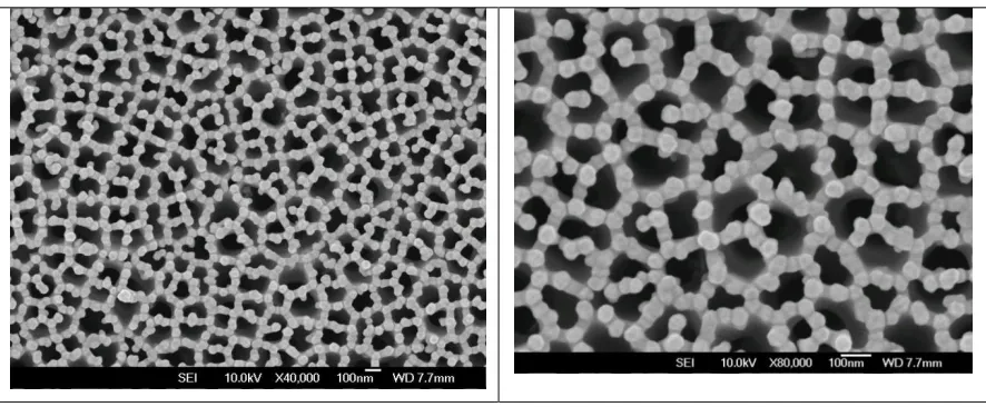
Figure 1. Field-emission SEM images of nanoporous gold electrode. The scale bar is 100 nm. The magnification is × 40000 and × 80000, respectively.
[image:5.596.77.520.469.652.2]
consists of nanoparticles in good homogeneity. It suggests that the deposited gold nanoparticles are in good crystalline structure, similar with that in the previous work [28]. Meanwhile, calculated from the images, the average diameter of gold nanoparticles and the “surface” filling factor are around 55.1 0.7 nm and 0.62 0.06, respectively. So, gold nanoparticles linked with each other along the AAO substrate frames and formed a compact structure. The special structure suggests that the physicochemical properties of nanoporous gold electrode would be affected not only by that of individual particles but also by their ring-shaped aggregates [28]. Compared to the conventional flat gold electrode, the individual particles and their linear and ring shaped aggregates make the nanoporous gold electrode possess larger active electrochemical area and higher conductivity, which facilitate the electron transfer and result in higher sensitivity for DNA sensing.
3.2. In-situ monitoring PNA/DNA hybridization
[image:6.596.159.439.295.693.2]
0.0 0.1 0.2 0.3 0.4
-100 0 100
I
(
A
.cm
-2 )
E (vs.SCE) a
b
[image:7.596.149.425.95.298.2]c
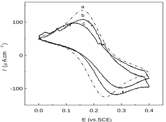
Figure 3. Cyclic Voltammograms of 1 mM Fe(CN)63-/4- on bare electrode (a), PNA-modified (b) and PNA/DNA-modified (c) nanoporous gold electrodes. 500 nM complementary DNA target was used for hybridization. Scan rate: 10 mV/s.
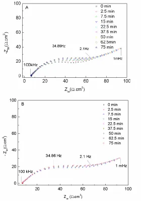
EIS is a simple and convenient method for in-situ kinetic study of PNA/DNA hybridization. Figure 2A shows the faradaic impedance spectra of PNA-modified nanoporous gold electrode in the presence of 500 nM complementary DNA target with different hybridization times. Since PNA is neutral and DNA possesses some negative charges (shown in Scheme 1), the electrode surface was turned from neutral to negative after hybridization. Obviously, the electron-transfer resistance (Rct), which is correlated to the diameter of Nyquist plot semicircle, increased gradually with increasing hybridization time.
It is consistent with the electrostatic repulsion of Fe(CN)63-/4- from the electrode interface by formation of negative charged PNA/DNA duplex, thereby introducing a barrier for interfacial electron transfer. Rct reached a plateau value after 75 minutes, indicating that the PNA/DNA hybridization reaction reached equilibrium. Impedance data for non-complementary DNA targets were shown in Figure 2B as control. No obvious change in semicircle was observed, indicating no hybridization reaction occurred for non-complementary DNA targets.
3.3. New equivalent circuit model
0 20 40 60 80
0 20 40 60 80
0 20 40 60 80 0 20 40 60 80
100 kHz
1.169 Hz
Zre(cm2)
-Z im
(
cm
2 )
100 kHz
1.169 Hz
[image:8.596.179.403.101.547.2]100 kHz 1.169 Hz
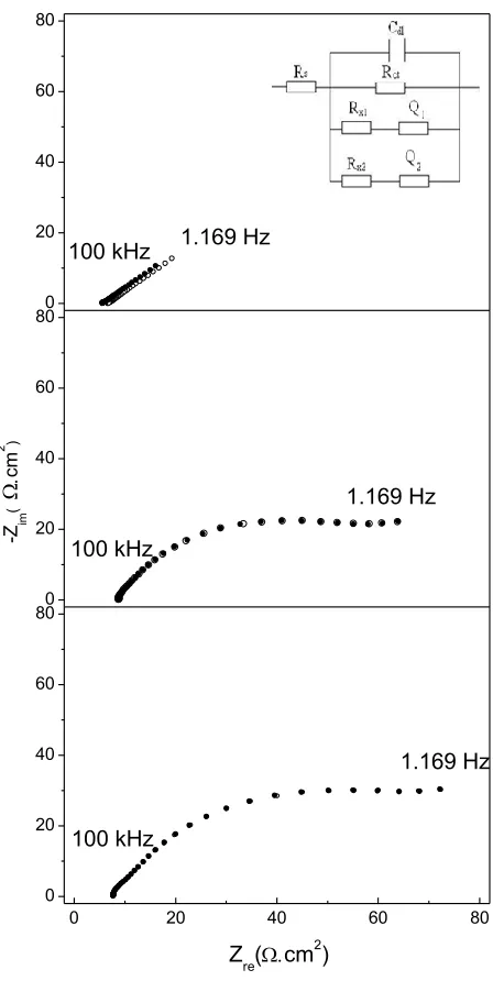
Figure 4. Representative Nyquist plots of bare (top), PNA-modified (middle) and PNA/DNA-modified (bottom) nanoporous gold electrodes in 50 mM PBS buffer containing 1mM/1mM Fe(CN)63-/4-. Measured data were shown as open circle and fitted data shown as solid ones. A new equivalent circuit model was shown in the inset figure. Rs: solution resistance; Cdl: double layer capacitance; Rct: charge-transfer resistance; Rx1: resistance through the PNA or PNA/DNA films; Rx2: pinhole/defect resistance; Q1, Q2: constant phase element.
[image:9.596.105.492.161.371.2]
corresponding to the electron-transfer-limited process was collected for data analysis. Data at lower frequency representing the diffusion-limited process is not shown in this work.
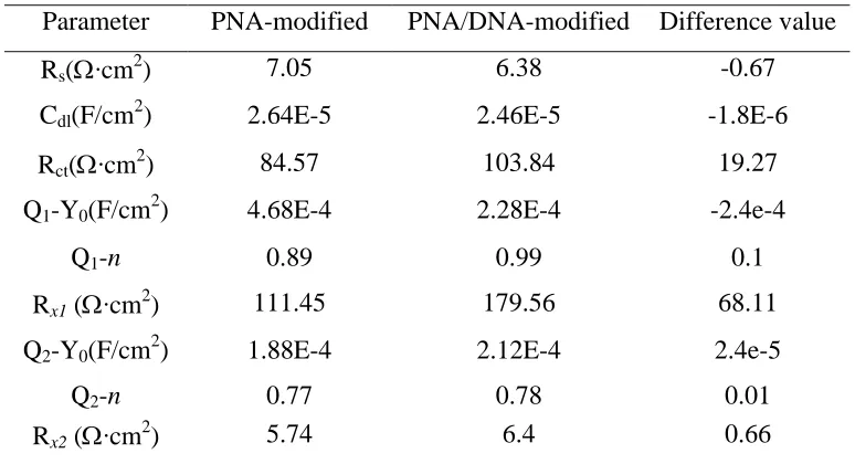
Table 2. Comparison of the fitting data analyzed by the new equivalent circuit model for PNA-modified and PNA/DNA-PNA-modified nanoporous gold electrodes
Parameter PNA-modified PNA/DNA-modified Difference value
Rs(∙cm2) 7.05 6.38 -0.67
Cdl(F/cm2) 2.64E-5 2.46E-5 -1.8E-6
Rct(∙cm2
) 84.57 103.84 19.27
Q1-Y0(F/cm2) 4.68E-4 2.28E-4 -2.4e-4
Q1-n 0.89 0.99 0.1
Rx1 (∙cm2) 111.45 179.56 68.11
Q2-Y0(F/cm2) 1.88E-4 2.12E-4 2.4e-5
Q2-n 0.77 0.78 0.01
Rx2 (∙cm2) 5.74 6.4 0.66
Complementary DNA target concentration: 200 nM
Fitted data was shown as solid line in Figure 4 and detail results were listed in Table 2. Considering the special structure of nanoporous gold electrode, reported Randles model for DNA/DNA duplex was not applicable [29, 30]. A new equivalent circuit model with paralleled (RQ) component was proposed in this work, shown in the inset figure of Figure 4. Electronic elements in the new equivalent circuit are described below. Solution resistance (Rs), is related to the resistance between reference electrode and working electrode. To minimize variations in Rs, the distance between the two electrodes was kept constant in all the measurements. The values of Rs for PNA and PNA/DNA films are almost similar, which range from 6 to 7 cm2. Cdl accounts for the double layer capacitance of the film on nanoporous gold electrode. The value for PNA/DNA film is a little smaller than that for PNA film. It may result from the increase in film thickness and charge repulsion force after PNA hybridized with DNA. Rx1 is related to resistance through PNA or PNA/DNA film; Rx2 is related to the pinhole/defect resistance of nanoporous gold electrode. The combination of Rx1 and constant phase element (Q1) accounts for resistance through PNA or PNA/DNA film. Q1 acts as a nonlinear capacitor related to film in homogeneity and electrode surface [31]. Values for Q1 range from 0.2 to 0.5 mFcm-2
3.4 DNA Sensing
5.0 5.5 6.0 6.5 7.0 7.5 8.0 0
20 40 60 80
0 100 200 300
Rct
(
cm
2 )
-log[C-DNA] (log [M])
R x1
(
.c
m
[image:10.596.156.420.120.333.2]2 )
Figure 5. The Relationship between resistances and complementary DNA target concentration.
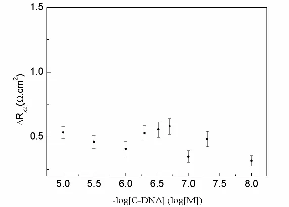
Figure 6. The Relationship between Rx2 and complementary DNA target concentration.
Generally, the charge-transfer resistance, Rct, is the key parameter, which varying with DNA target concentration. Meanwhile, in the new equivalent model, Rx1 increases with the increase of DNA concentration. Therefore, both Rct and Rx1 were plotted with DNA concentration, shown in Figure 5. Meanwhile, the relationship between Rx2 and DNA concentration was plotted as Figure 6.
[image:10.596.156.442.395.600.2]
DNA concentration. The reason is that Rx2 is only related to the pinhole/defect resistance in the electrode. No defect site formed during PNA/DNA hybridization process. The detectable concentration of complementary DNA is 10 nM using Rx1 as response factor. The sensitivity for PNA-modified electrode is 0.4 /cm2nM, which is higher than that reported in the literature [32].
The DNA sensing performance in this work was compared with those in recent reports using other techniques. Results were listed in Table 3. Obviously, flurometric method is more sensitive for DNA sensing [2, 33]. However, output signal is not so stable because the fluorescent marker is easier to quench in detection process. Meanwhile, flurometric method is involved fluorescent marker-labeling, which is tedious and time-consuming. Lower detectable DNA concentrations were obtained in other works utilizing electrochemical techniques such as CV, ADPV and DPV [34, 35], in which indicator and electrode pretreatment must be used for signal acquiring process. It should be noted that the detection limit was measured to 10 nM using Rx1 as response factor in this work. The value is lower than that reported on boron-doped diamond (BDD) electrode using the EIS technique [36], which involved BDD electrode modification process of polyaniline/polyacrylate layer. The value (10 nM) is same with that on similar working electrode-nanoporous gold electrode reported in reference [37]. In that report, SWV technique was adopted, in which the indicator of methylene blue had to be used. In this work, no label and no indicator are in need. Therefore, a methodology for rapid, sensitive and label-free detection of DNA has been set-up based on nanoporous gold electrode in this work. Additionally, it should be noted that the sensor discussed in this work was not optimized for lower detection limit. It can be significantly improved by reducing electrochemical cell volume (e.g., microfluidics) and electrode size to optimize target-to-electrode transport and reaction rates.
Table 3. Comparison of DNA sensing in some reports with that in this work Sensing
Substrate
Label/Indicator Probe Modified layer/ Pretreatment
Detection Method
Stability LOD (nM)
Ref.
NA Ce(QS)2Cl DNA None Flurometric Poor 0.07 [2]
Etched optical fiber
bi-p,p’
-4-Hydroxyphenylac etic acid
DNA Streptavidin labeled horseradish peroxidase
Flurometric Poor 0.001 [33]
CPE Methylene blue DNA Zirconia CV/DPV Common 0.2 [34]
PGE None DNA Pretreatment in
acetate buffer
ADPV Common 0.069 [35]
BBDE None DNA Polyaniline/Polyacrylate EIS Good 20 [36]
NGE Methylene blue DNA None SWV Good 10 [37]
NGE None PNA None EIS Excellent 10 TW
ADPV: anodic differential pulse voltammetry; DPV: differential pulse voltammetry; SWV: square wave voltammetry; CV: cyclic voltammetry; CPE: Carbon paste electrode; BBDE: Boron-doped diamond electrode; PGE: Pencil graphite Electrode; NGE: Nanoporous gold electrode; TW: this work; NA: not applicable.
4. CONCLUSION
component was proposed for nanoporous gold electrode. Rx1 is related to resistance through PNA or PNA/DNA film; Rx2 is related to the pinhole/defect resistance of nanoporous gold electrode. It is worth to be noticed that Rx1 increased faster than that in charge transfer resistance with the increase of DNA concentration. Therefore, using Rx1 as the response factor, sensitivity of 0.4 /cm2nM and detectable concentration of complementary DNA 10 nM were obtained on the nanoporous gold electrode.
ACKNOWLEDGEMENT
This work was supported by the National Natural Science Foundations of China (No. 21405106), the Foundation for Distinguished Young Talents in Higher Education of Guangdong, China (No. 2014KQNCX130), the Natural Science Foundation of Shenzhen University (No. 827-000022), and the Research and Development Foundation of Science and Technology of Shenzhen (Nos. JCYJ20150324141711592 and JCYJ20170302145633009).
References
1. R. M. Hawk, M. V. Chistiakova and A. M. Armani, Opt. Lett., 38 (2013) 4690.
2. M. Shamsipur, Z. Memari, M. R. Ganjali, P. Norouzi and F. Faridbod, J. Pharm. Biomed. Anal., 118 (2016) 356.
3. Y. Fan, K. Hotta, A. Yamaguchi, Y. Ding and Y. He, Appl. Phys. Lett.,105 (2014) 031103. 4. M. J. Walker and R. Rapley, Molecular Biology and biotechnology, The Royal Society of
Chemistry. Thomas Graham House, 2000, Cambridge, U.K.
5. M. Berggren and A. Richter-Dahlfors, Adv. Mater., 19 (2007) 3201.
6. X. J. Zheng, J. D. Qiu, L. Zhang, Z. X. Wang and R. P. Liang, Chem. Commun., 49 (2013) 3546. 7. A. S. Patterson, K. Hsieh, H. T. Soh and K. W. Plaxco, Trends Biotechnol., 31 (2013) 704. 8. H. Gaiji, P. Jolly, S. Ustuner, S. Goggins and M. Abderrabba, Electroanalysis, 28 (2016) 1. 9. J. D. Besant, I. B. Burgess, W. H. Liu, E. H. Sargent and S. O. Kelley, Nat. Commun., 22 (2015)
6978.
10.S. Kelley, R. Gasparac, M. Lapierre-devlin and B. Taft, Electrocatalytic nucleic acid hybridization detection. US20040913925 [P] 2004-08-06.
11.P. M. Sabale, J. T. George and S. G. Srivatsan, Nanoscale, 6 (2014) 10460. 12.Y. Wang, C.J. Li, X. H. Li, Y. F. Li and H. Kraatz, Anal. Chem., 80 (2008) 2255. 13.J. Weng, J. Zhang, H. Li, L. Sun, C. Lin and Q. Zhang, Anal. Chem., 80 (2008)7075.
14.14.Y. Park, S. Kim, I. H. Jang, Y. S. Nam, H. Hong, D. Choi and W. G. Lee, Analyst, 1 (2016) 451.
15.W. Shi, Y. Q. Shen, D. T. Ge, M.Q. Xue, H. H. Cao, S. Q. Huang, J. X. Wang, G. L. Zhang, and F. B. Zhang, J. Membrane Sci., 325 (2008) 801.
16.F. Liu, J. Y. Lee and W. J. Zhou, Small, 2 (2006) 121.
17.A. Santos, T. Kumeria and D. Losic, Trends Anal. Chem., 44 (2013) 25.
18.P. Ciambelli, L. Arurault, M. Sarno, S. Fontorbes, C. Leone, L. Datas, D. Sannino, P. Lenormand and S. Le Blond Du Plouy, Nanotech., 22 (2011) 265613.
19.F. Li, L. Zhang and R. Metzger, Chem. Mater., 10 (1998) 2470.
20.C. C. Lu, Y.S. Huang, J. W. Huang, C. K. Chang and S. P. Wu, Sensors, 10 (2010) 670. 21.H. Masuda and K. Fukuda, Science, 268 (1995) 1466.
22.H. Masuda and M. Satoh, Jpn. J. Appl. Phys., 35 (1996) L126.
23.H. Masuda, K. Yada and A. Osaka, Jpn. J. Appl. Phys., 37 (1998) L1340.
25.Y. Piao, H. Lim, J. Y. Chang, W. Y. Lee and H. Kim, Electrochim. Acta, 50 (2005) 2997. 26.H. Su, Y. Li, X.Y. Li and K. S. Wong, Opt. Express, 17 (2009) 22223.
27.Y. J. Kim, J. E. Jones, H. Li, H. Yampara-Iquise, G. L. Zheng, C. A. Carson, M. Cooperstock, M. Sherman and Q. S. Yu, J. Electroanal. Chem., 702 (2013) 72.
28.Y. S. Li, H. M. Su, K .S. Wong and X. Y. Li, J. Phys. Chem. C., 114 (2010) 10463. 29.Y. T. Long, C. Z. Li, H. B. Kraatz and J. S. Lee, Biophys. J., 84 (2003) 3218. 30.X. Li, J .S. Lee and H. B. Kraatz, Anal. Chem., 78 (2006) 6096.
31.M. Dijksma, B. A. Boukamp, B. Kamp and W. P. Bennekom, Langmuir, 18 (2002) 3105. 32.A. Kukol, P. Li, P. Estrela, P. K.o-Ferrigno and O. Migliorato, Anal. Biochem., 374 (2008) 143. 33.S.Y. Niu, Q.Y. Li, R. Ren and S.S. Zhang, Biosens. Bioelectron., 24 (2009) 2943.
34.S.H. Zuo, L. F. Zhang, H. H. Yuan, M. B. Lan, G. A. Lawrance and G. Wei, Bioelectrochemistry, 74 (2009) 223.
35.M. H. Pournaghi-Azar, E. Alipour, S. Zununi, H. Froohandeh and M. S. Hejazi, Biosens. Bioelectron., 24 (2008) 524.
36.H.R. Gu, X.D. Su and K. P. Loh, J. Phys. Chem. B, 109 (2005) 13611. 37.P. Daggumati, Z. Matharu and E. Seker, Anal. Chem., 87 (2015) 8149.