Abstract— Residue Number System (RNS) is often used in Cryptographic applications. Choice of a unique base for RNS is an important factor in implementing RNS. Bit folding after multiplication is a commonly used method for implementing RNS. In this paper an architecture based on modulo 2n-3 arithmetic is implemented. Each word of partial product is mapped once normal and then with one bit left shift with reference to the base number. The results are tabulated in terms of delay and area with Xilinx tool. Efficiency of implementation is compared with results available in literature.
Keywords— Modulo Arithmetic, Residue Number System, Squarer.
I. INTRODUCTION
Various choices of moduli for modulo arithmetic have been considered in recent literature. Several authors have considered power of two related moduli such as 2n, 2n-1and 2n+1 in their works, e.g., Szabo and Tanaka [1], Soderstrand et al.[2], P.V.Ananda Mohan [3] and A.R.Omondi [4]. Other moduli such as 2n-3, 2n+3 have gained importance due to their ease in performing multiplication operation. Few authors viz., Sheu et al. [5], P.V. Ananda Mohan [6] and Muralidharan and Chang [7] have worked on four moduli set {2n-1, 2n+1, 2n-3, 2n+3} for developing efficient RNS-to-binary reverse converters. However design of forward binary-to-RNS converters for the moduli 2n-3, 2n+3 have been investigated by Adamdis and Vergos[8], Spyrou et al[9], Strollo and Caro[10], and others. Majority of the literature is focused on multipliers. Squarers with modulo 2n+1 designed by Vergos and Efstathiou[11] have received due consideration. Squarers based on moduli 2n-3, 2n+3 have received very less attention. Although multipliers can be used for squaring operation, specialized squarer is frequently used in cryptography and therefore need attention.
A modulo 2n-3 squarer has been implemented and reported in this paper. Design of the squarer is presented in section II. Implementation and results are presented in sections III and IV respectively. Section V concludes the paper. References are listed in section VI.
Revised Manuscript Received on December 12, 2019.
* Correspondence Author
Nagaraj Aiholli*, E&C , KLECET, Belagavi 590008 ,India [email protected]
Uday Wali, C-Quad Research, Desur IT Park, Belagavi, 590014 India, [email protected]
Rashmi Rachh, CS, VTU Post Graduate Studies, Belagavi-590010 India, [email protected]
II. NOVELSQUARERSBASEDONMODULO2N-3
Multiplication of two n-bit numbers results in a product of (2n-1) bits. Partial products obtained during multiplication
range from n bits to (2n-1) bits. In each partial product word, bits beyond n bit are (rotated) mapped once normal and then with one bit left shift. For example, for n = 5, 2n-3=29, mapping of partial product word 0 1001 0011 = 147 can be represented as
1 0011 = 19 mod 29 = 19
0100 = 4 mod 29 = 4
01000 = 8 mod 29 = 8
[image:1.595.315.556.466.842.2]All the partial product words after mapping are converted into their equivalent decimal number in terms of bits. These bits are added using a carry save adder (CSA) tree followed by a carry propagate adder at the final stage. A modulo 2n-3 operation on the output of final stage will give the square of the input number. The proposed squarer has various stages shown in the block diagram in below Fig.1. This approach for squarers has been described in literature. Fig 2(a) shows the partial product bits after multiplication of the input with itself. Fig 2(b) indicates the bits after mapping and rearranging the partial product bits in the matrix.
Fig. 1. Block diagram showing steps used in proposed squarer design
(a)
a3a0 a2a0 a1a0 a0a0
a2a1 a1a1 a1a0 a3a1
a2a1 a2a0 a3a2 a2a2
a3a0 a3a3 a3a2 a3a1
a3a3 a3a2 a3a1 a3a2 a2a2 a3a1
Depth 5 6 7 4
(b)Fig.2. Bit matrices (a) of a 4×4 bit multiplier and (b) after reduction mod 13.
Implementation of Arithmetic unit for RNS
using 2
n
-3 as Base
Nagaraj.Aiholli, Uday.Wali , Rashmi.Rachh
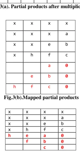
Fig 3(a) illustrates partial products matrix for mod 13 squarer of a 4 bit number. Fig 3(b) shows partial products after mapping. It may be noted that are original bits below fourth bit position which need not be rewritten. Fig 3(c) shows the bits after rearranging respectively. Bits in Fig.3 (b) are packed to yield Fig.3(c). Partial products are obtained with conventional method of multiplication. Bits beyond 4 bits for 4 bit squarer are mapped once normal and then with one bit left shift as illustrated in Fig.2(b). Bits are then packed vertically. Final row shows depth of each column.
x x x x
a x x x
e b x x
h f c x
Fig. 3(a). Partial products after multiplication
x x x x
x x x a
x x e b
x h f c
a 0
e b 0
h f c 0
Fig.3(b).Mapped partial products
Fig. 3(c). Rearranged partial products
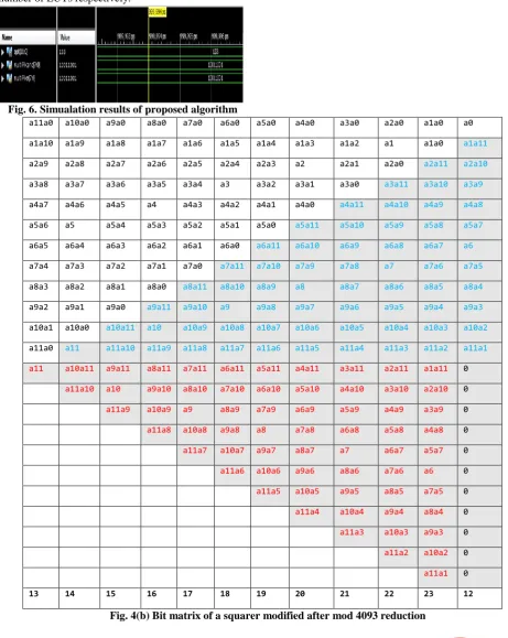
Each row of bits is converted into its decimal equivalent in terms of bit vector. Each word is reduced with the modulo operation. Bits are then added with a CSA tree. In the first row of full adders, top three rows are added and then one row at a time. If no bits are remaining to be added, we stop that column at that level. The final sum and carry vectors are added using a 4-bit Carry Propagate Adder (CPA). The sum so obtained is subjected to final modulo reduction. The resulting value is equivalent to that obtained from conventional approach. Same approach is extended to 8 bit (mod 253) and 12 bit (mod 4093) squarer respectively. These are depicted in Fig.4(a) and 4(b) respectively. (Fig.4(b) is on next page.) A flowchart with the steps of algorithm is shown in Fig. 5.
a7a0 a6a0 a5a0 a4a0 a3a0 a2a0 a1a0 a0 a6a1 a5a1 a4a1 a3a1 a2a1 a1 a1a0 a7a1
a5a2 a5a1 a5a0 a7a5 a6a5 a5 a5a4 a5a3 a6a1 a6a0 a7a6 a6 a6a5 a6a4 a6a3 a6a2 a7a0 a7 a7a6 a7a5 a7a4 a7a3 a7a2 a7a1 a7 a7a6 a7a5 a7a4 a7a3 a7a2 a7a1 0 a7a6 a6 a6a5 a6a4 a6a3 a6a2 0 a7a5 a6a5 a5 a5a4 a5a3 0 a7a4 a6a4 a5a4 a4 0 a7a3 a6a3 a5a3 0 a7a2 a6a2 0
a7a1 0
9 10 11 12 13 14 15 8
Fig.4(a) Bit matrix of a squarer modified after mod 253 reduction
Jaberipur et al[19] have considered two vectors {l,h} and {l’,h’}. Vectors h, 2h, h’ and 2h’ are added which require multiplication by 3. Another approach for modulo 2n-3 multiplier is described by Matutino et al[20]. He illustrates his work by an equation
(AxB) 2 n
-3 = (3.P1 + P0) 2 n
-3 (1) where P0 are the original bits and 3.P1 is after mapping once normal and then with one bit left shift. Jaberipur[19] and Matutino[20] have worked on multiplication of two inputs using modulo operation. Their work is related to modulo reduction of the partial product bits. However, their procedure requires modulo reduction of every word and hence slower. Our procedure requires modulo operation to be performed only once on the final sum to get the square of given input.
Fig. 5.Flowchart of squarer
x x x x
x x x a
x x e b
x h f c
[image:2.595.308.548.48.208.2] [image:2.595.76.262.176.269.2] [image:2.595.91.244.254.543.2] [image:2.595.346.515.406.800.2]III. SOFTWAREIMPLEMENTATIONAND TESTING
We have used Xilinx ISE design suite 14.7 as a design tool with programming done in verilog. Implementation of the proposed algorithm has been synthesized using the same tool. The target implementation device is a Xilinx FPGA viz., Virtex 6 XC6VLX75T in FF484 package and -3 speed grade, under the Xilinx ISE 14.7 working environment.
[image:3.595.59.521.179.759.2]The Integrated SIM is used for the behavioral verification. The speed is measured in terms of delay and the area in terms of number of LUTsrespectively.
Fig. 6. Simualation results of proposed algorithm
The simulation waveform is shown above. Values of multiplicand and multiplier used for simulation are:
multiPlicand[7:0] = 10011001 = 15310; multiPlier[7:0] = 10011001 = 15310; Expected result of the squarer is
153x153 = 23409 = 133 mod 253 which is observed in Fig. 6 above as
Opt[12:0] = 10000101=133(decimal). The RTL schematic obtained using the Xilinx tool is represented in Fig.7.
a11a0 a10a0 a9a0 a8a0 a7a0 a6a0 a5a0 a4a0 a3a0 a2a0 a1a0 a0
a1a10 a1a9 a1a8 a1a7 a1a6 a1a5 a1a4 a1a3 a1a2 a1 a1a0 a1a11
a2a9 a2a8 a2a7 a2a6 a2a5 a2a4 a2a3 a2 a2a1 a2a0 a2a11 a2a10
a3a8 a3a7 a3a6 a3a5 a3a4 a3 a3a2 a3a1 a3a0 a3a11 a3a10 a3a9
a4a7 a4a6 a4a5 a4 a4a3 a4a2 a4a1 a4a0 a4a11 a4a10 a4a9 a4a8
a5a6 a5 a5a4 a5a3 a5a2 a5a1 a5a0 a5a11 a5a10 a5a9 a5a8 a5a7
a6a5 a6a4 a6a3 a6a2 a6a1 a6a0 a6a11 a6a10 a6a9 a6a8 a6a7 a6
a7a4 a7a3 a7a2 a7a1 a7a0 a7a11 a7a10 a7a9 a7a8 a7 a7a6 a7a5
a8a3 a8a2 a8a1 a8a0 a8a11 a8a10 a8a9 a8 a8a7 a8a6 a8a5 a8a4
a9a2 a9a1 a9a0 a9a11 a9a10 a9 a9a8 a9a7 a9a6 a9a5 a9a4 a9a3
a10a1 a10a0 a10a11 a10 a10a9 a10a8 a10a7 a10a6 a10a5 a10a4 a10a3 a10a2
a11a0 a11 a11a10 a11a9 a11a8 a11a7 a11a6 a11a5 a11a4 a11a3 a11a2 a11a1
a11 a10a11 a9a11 a8a11 a7a11 a6a11 a5a11 a4a11 a3a11 a2a11 a1a11 0
a11a10 a10 a9a10 a8a10 a7a10 a6a10 a5a10 a4a10 a3a10 a2a10 0
a11a9 a10a9 a9 a8a9 a7a9 a6a9 a5a9 a4a9 a3a9 0
a11a8 a10a8 a9a8 a8 a7a8 a6a8 a5a8 a4a8 0
a11a7 a10a7 a9a7 a8a7 a7 a6a7 a5a7 0
a11a6 a10a6 a9a6 a8a6 a7a6 a6 0
a11a5 a10a5 a9a5 a8a5 a7a5 0
a11a4 a10a4 a9a4 a8a4 0
a11a3 a10a3 a9a3 0
a11a2 a10a2 0
a11a1 0
13 14 15 16 17 18 19 20 21 22 23 12
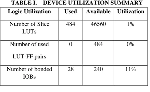
TABLE I. DEVICE UTILIZATION SUMMARY
IV. SIMULATIONRESULTS
The device utilization summary report shows the number of LUTs utilized. The device summary report also gives number of LUT pairs and some of IO blocks used. The total gate delay is 22.188ns. As compared to the delay obtained in the proposed work for the squarer, that by Jaberipur [19] for an 8 bit multiplication is 6.4ns. Hence the results of work in this paper are comparable to that of Jaberipur in terms of delay. The xpower analyzer tool is used to calculate power consumption of the circuit which is about 1.293W.
We have not been able to provide any comparative statement on performance of the squarer as there is no published literature on squarers designed specifically for modulo 2n-3 RNS.
V. CONCLUSION
The main focus of this paper is to implement a squarer for 2n-3 modulo RNS. The design demonstrated here shows 8 and 12 bit units but also works for quite higher number of bits. The future work may be to implement the design on Virtex-7 FPGA and Virtex-6 low power design FPGA. Main focus of this research is to show that a method exists whose results are comparable to the results by Jaberipur [19] in terms of delay. While the initial studies are already more efficient than that reported in literature, there is ample scope to improved low power and speed performance of the design.
REFERENCES
1. N. Szabo and R. Tanaka,” Residue Arithmetic and Its applications in Computer Technology”, McGraw Hill, 1967.
2. M.A. Soderstrand, G.A. Jullien, W.K. Jenkins and F. Taylor, (Eds), “Residue Number System Arithmetic: Modern Applications in Digital Signal Processing”, IEEE Press,1986.
3. P.V. Ananda Mohan, “Residue Number Systems: Algorithms and Architectures”, Kluwer, 2002.
4. A.R. Omondi, A.B. Premkumar, “Residue Number Systems: Theory and implementation”, (Imperial College Press, 2007) 5. M.H. Sheu, S.H. Lin, C. Chen and S.W. Yang, “An efficient VLSI
design for a residue to binary converter for general Balance moduli (2n-3, 2n-1, 2n+1, 2n+3)”, IEEE Transactions on Circuits and Systems, Express Briefs, 2004, Vol. 51, pp 52- 55, 2004. 6. P.V. Ananda Mohan, “New Reverse converters for the moduli set
{2n-3, 2n+1, 2n-1, 2n+3}”, AEU, 2008, Vol.62, pp 643-658, 2008.
7. R. Muralidharan and C.H. Chang,” Fixed and variable
8. D. Adamidis and H.T. Vergos,”RNS
multiplication/sum-of-squares Units”, IET computers Digit Tech, Vol. 1, pp. 38-48, 2007.
9. A. Spyrou, D. Bakalis and H.T. Vergos, “Efficient architectures for modulo 2n-1 squarers”, Proc. IEEE International Conference on
DSP 2009, pp. 1-6, 2009.
10. A. Strollo and D. Caro,” Booth Folding encoding for high performance Squarer circuits”, IEEE Transactions on CAS, Part II, Vol.50, pp. 250- 254, 2003.
11. H.T. Vergos and C. Efstathiou,” Efficient modulo 2n+1squarers”, Proc. XXI Conference on Design of Circuits and Integrated systems, DCIS, 2006
12. R. Muralidharan, C.H. Chang and C. Jong,” A low complexity modulo 2n+1 squarer design”, Proc. IEEE Asia Pacific conference on Circuits and Systems, pp. 1296-1299, 2008.
13. H.T. Vergos, C. Efstathiou, “Diminished-1 modulo 2n+1 squarer design”, Proc.IEE Comput. Digi. Tech, Vol.152, pp.561-566, 2005.
14. D. Bakalis, H.T. Vergos and A. Spyrou,” Efficient modulo 2n±1squarers”, Integration, the VLSI journal, Vol.44, pp. 163-
174, 2011.
15. D. Bakalis and H.T. Vergos, “Area-efficient multi-moduli squarers for RNS”, Proc. 13th Euromicro conference on Digital SystemDesign: Architectures, methods and Tools, pp. 408-411, 2010.
16. B. Cao, T. Srikanthan and C.H. Chang, “A new design method to modulo 2n-1 squaring”, Proc. ISCAS, pp. 664- 667, 2005.
17. A.E. Cohen and K.K.Parhi, “Architecture Optimizations for the RSA Public Key Cryptosystem: A Tutorial”, IEEE Circuits and Systems Magazine, Vol. 11, pp.24 – 34, 2011.
18. H. Pettenghi, R. Chave and L. Sousa, “Method for designingmodulo {2n±k} binary to RNS converters’’, Proceedings of the Conference on Design of Circuits and integrated Systems, DCIS, 2013.
19. Ahmadifar. H. and Jaberipur. G. ”Improved modulo -(2n+3)multipliers”, International Symposium on Computer
Architecture and Digital Systems, (CADS), pp.31-35, 2013. 20. Pedro. M. Matutino, R. Chaves and L. Sousa,” Arithmetic units for
RNS Moduli {2n-3} and {2n +3} operations”, 13th Euromicroconference on Digital System Design: Architectures, methods and Tools, 2010.
21. L. Huihua, L.Lei and Z. Wanting, “High-Speed and High-efficient Modulo (2n-3) Multipliers”, International Conference on
Education, Management, Computer And Society (EMCS 2016). 22. Nagaraj.Aiholli, Rashmi Rachh, Uday.Wali, “Design of
Arithmetic unit for RNS using 2n-3 as Base”, International
Conference on Electrical, Electronics, Communication, Computer Technologies and Optimization Techniques (ICEECCOT 2018), In Press.
23. Siva.S.Sinthura, Afreen Begum et al, “Implementation and Analysis of different 32-bit multipliers on aspects of Power, Speed and Area”, Interenational Conference on Trends in Electronics and Informatics(ICOEI 2018).
24. Manoj.Sharma, Richa.verma, “Disposition(reduction) of (negative) partial product for 4 Booth’s Algorithm”, World Congress on Information and Communication Teechnologies, 2011.
AUTHORSPROFILE
Nagaraj.R.Aiholli received his B.E degree from BVB College of Engineering and Technology, Hubli. He graduated with MTech degree from Visvesvaraya Technological University, Belagavi. He is currently pursuing his PhD from Dr.M.S.Sheshagiri’s KLE College of Engineering and Technology, Belagavi under the banner of Visvesvaraya Technological University, Belagavi. He is presently working as Assistant Professor in Electrical department at Jain College of Engineering, Belagavi. He has more than 16 years of teaching experience. He has published a paper in international journal and presented paper in two International conferences including IEEE. His Logic Utilization Used Available Utilization
Number of Slice LUTs
484 46560 1%
Number of used
LUT-FF pairs
0 484 0%
Number of bonded IOBs
Uday Wali is a Professor in Dept. of EEE at KLE Dr M S Sheshgiri College of Engineering. & Technology, Belagavi, Karnataka India. He has obtained Bachelor of Engineering in Electrical and Electronics Engg. from Karnataka University Dharwad (1981) and Ph.D from IIT Kharagpur (1986). He is a fellow of Institute of Engineers (India) and CEO of C-Quad Computers, Desur IT Park, Belagavi. He has 30 years of teaching and 15 years of industrial experience. His current research interests are Artificial Intelligence, Neural Networks, and Processor Design.
[image:5.595.49.261.161.597.2]Dr Rashmi Rachh graduated in Electrical Engineering from Karnatak University Dharwad. She obtained her M.Tech from Manipal and PhD from Visvesvaraya Technological University, where she is currently a professor. She has received best paper awards in national and international conferences. Her research interests are Cryptography, Data Science, Analytics and Artificial Intelligence.