Rochester Institute of Technology
RIT Scholar Works
Theses Thesis/Dissertation Collections
12-6-2017
Modeling and Implementation of HfO2-based
Ferroelectric Tunnel Junctions
Spencer Allen Pringle
Follow this and additional works at:https://scholarworks.rit.edu/theses
This Thesis is brought to you for free and open access by the Thesis/Dissertation Collections at RIT Scholar Works. It has been accepted for inclusion in Theses by an authorized administrator of RIT Scholar Works. For more information, please [email protected].
Recommended Citation
Modeling and Implementation of HfO
2-based
Ferroelectric Tunnel Junctions
Spencer Allen Pringle
December 6, 2017
A Thesis Submitted in Partial Fulfillment
of the Requirements for the Degree of Master of Science
in
Microelectronic Engineering
Spencer Allen Pringle
Committee Approval:
We, the undersigned committee members, certify that Spencer Pringle has completed the requirements for the Master of Science degree in Microelectronic Engineering.
Dr. Santosh KurinecAdvisor Date
Professor, Microelectronic Engineering
Dr. Dhireesha Kudithipudi Date
Professor, Computer Engineering
Mr. Mark Indovina Date
Lecturer, Electrical Engineering
Dr. Robert Pearson Date
Programs Director, Microelectronic Engineering
Dr. Sohail Dianat Date
Acknowledgments
The author would like to thank Dr. Santosh Kurinec for being consistently helpful, encouraging, and supportive throughout the completion of this work. Her helpful advice and fruitful discussions of quantum mechanics were always productive. Huge thanks to Mr. Mark Indovina for assitance implementing address systems and other system design. Many thanks to Dr. Dhireesha Kudithipudi for help learning and understanding the implementation of FTJ devices in neuromorphic systems and the many applications of such architectures. Also, many thanks to NamLAB and the University of California, Berkeley, for agreeing to deposit their own ferroelectric films for further implementation and testing of ferroelectric tunnel junctions.
This work was supported in part by the National Science Foundation, Grant# ECCS-1541090. Any opinions, findings, and conclusions or recommendations ex-pressed in this material are those of the author and do not necessarily reflect the views of the National Science Foundation.
inspiration to keep striving to be a better person.
Abstract
HfO2-based ferroelectric tunnel junctions (FTJs) represent a unique opportunity as
both a next-generation digital non-volatile memory and as synapse devices in brain-inspired logic systems, owing to their higher reliability compared to filamentary resistive random-access memory (ReRAM) and higher speed and lower power con-sumption compared to competing devices, including phase-change memory (PCM) and state-of-the-art FTJ. Ferroelectrics are often easier to deposit and have simpler material structure than films for magnetic tunnel junctions (MTJs). Ferroelectric HfO2 also enables complementary metal-oxide-semiconductor (CMOS) compatibility,
since lead zirconate titanate (PZT) and BaTiO3-based FTJs often are not.
No other groups have yet demonstrated a HfO2-based FTJ (to best of the author’s
knowledge) or applied it to a suitable system. For such devices to be useful, system designers require models based on both theoretical physical analysis and experimental results of fabricated devices in order to confidently design control systems. Both the CMOS circuitry and FTJs must then be designed in layout and fabricated on the same die.
This work includes modeling of proposed device structures using a custom python script, which calculates theoretical potential barrier heights as a function of material properties and corresponding current densities (ranging from 8×10³ to 3×10⁻² A/cm2
with RHRS/RLRS ranging from 5×10⁵ to 6, depending on ferroelectric thickness).
Signature Sheet i
Abstract iv
Table of Contents v
List of Figures viii
List of Tables xi
List of Symbols xii
1 Introduction 1
1.1 Research objectives . . . 2
1.2 Thesis organization . . . 2
1.3 Neuromorphic Computing with Memristors, ReRAM . . . 4
1.4 Using Ferroelectric Tunnel Junctions . . . 5
2 Physics of Ferroelectric Materials 6 2.1 Crystal structure . . . 6
2.2 Polarization in ferroelectrics and dielectrics . . . 7
2.3 Non-intrinsic ferroelectrics . . . 8
2.4 Ferroelectric domains . . . 9
2.5 Area-dependent effects . . . 9
3 Brief History and Applications of FTJ Implementations 11 3.1 Early memory using large-dimension PZT . . . 11
3.2 More recent implementations with BaTiO3 . . . 11
3.3 Applications of FTJs . . . 13
3.4 Alternative technologies . . . 14
3.4.1 Filamentary ReRAM . . . 14
3.4.2 Magnetic tunnel junctions . . . 15
CONTENTS
4 Analysis of M1-Fe-M2 Structure 17
4.1 Band structure in the absence of polarization field . . . 17
4.2 Band structure under polarization . . . 18
4.3 Extraction of tunnel Current and (by extension) resistance states . . 21
5 Design of Ferroelectric HfO2-based FTJs and Integration with CMOS Process 23 5.1 FTJ design . . . 23
5.2 State of the art FTJs . . . 26
5.3 Designed CMOS-process with FTJ-fabrication steps . . . 28
5.4 Process simulation . . . 36
6 System Design and Simulations for Digital Memory Applications 38 6.1 Read/Write scheme . . . 38
6.2 Linear resistance change simulation . . . 40
6.3 Timing-based simulation . . . 41
6.4 Address systems . . . 43
6.5 Simulation results - 4×4 Array . . . 45
7 Conclusions 50 7.1 Future Work . . . 51
A Python Program Code 59 A.1 Core Code . . . 59
A.2 GUI Code . . . 78
B Partial Process - FTJ-devices only 90 C Athena code 93 D sap1951 FTJ THESIS 45 97 D.1 Linear Resistance FTJ Model . . . 97
D.1.1 Verilog Model . . . 98
D.2 Polarization-Timing FTJ Model . . . 101
D.2.1 Verilog Model . . . 102
D.3 SAP ADDRESS COLUMN R . . . 115
D.4 SAP ADDRESS COLUMN W . . . 118
D.6 SAP ADDRESS ROW W . . . 124
D.7 SAP ADDRESS GND vcc . . . 127
D.8 SAP FTJ DIGITAL LOW 4 x 4 . . . 130
D.9 SAP TRISTATE MEM 4x vcc . . . 132
D.10 SAP TRISTATE MEM 4x TESTBENCH . . . 134
List of Figures
1.1 Diagram representation of the dependencies of various implementation stages of the technology presented in this thesis. . . 3 2.1 Ferroelectric polarization (a) and weak magnetic moment (b) of
multi-ferroic Bi2NiMnO6 at 7K, from Shimakawa et. al [1]. The red line on
(a) is what this plot would look like for a perfect dielectric. . . 7 2.2 Simple representation of the atomic structures of a ferroelectric as its
prototype phase (left) relaxes into one of two polar phases (middle and right) after the application of an external field. A ferroelectric would remain in the corresponding state even after the removal ofEapp, while
a dielectric would deflect (as shown) during stimulus application but relax to the non-polar phase (left) once that field was removed. . . 7 2.3 Simple diagram of domains in a model ferroelectric film. . . 9 3.1 ”Bender memory” schematic from [2]. This 8-bit device stores data
as remanent polarization in the top-most ferroelectric material. Write pulse is≈1 ms of 20-30 V/mil. . . 12 3.2 Performance of FTJs for (a) fresh device with PZT ferroelectric and
(b) device with BaTiO3 ferroelectric after -1.2V priming pulse, taken
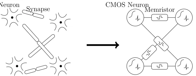
from Contreras et. al [3]. . . 13 3.3 Simple diagram of (left) a physical model of neurons and synapses, the
brain’s computation devices, and (right) their electronic implementa-tion in a typical brain-inspired computing system. . . 15 4.1 The energy band diagram of an metal-insulator-metal (MIM) with a 2
nm thick insulator with Ea = 2 eV and metals having χ1 = 4.08 eV,
χ2 = 4.85 eV, normalized to the fermi energy. . . . . 18 4.2 The Fowler-Nordheim tunneling current of an MIM with material
prop-erties listed in Section 4.1. . . 19 4.3 (a) Diagram of charge densities created for left polarized ferroelectric
4.4 The energy band diagrams, at V = 0, of an FTJ with material prop-erties given in Section 4.2, for positive (towards electrode 1 (M1)) and negative (towards electrode 2 (M2)) polarization. . . 21 4.5 The Fowler-Nordheim tunneling current of an FTJ with material
prop-erties consistent with those used in Figure 4.4, showing a memory win-dowHRS/LRS ≈2.3. . . 22 5.1 Simulated HRS/LRS increases with larger screening length ratio before
plateauing around δ2
δ1 ≈60. For an Al/Al:HfO2/p+ Si FTJ with 2 nm
ferroelectric. . . 24 5.2 Simulated HRS/LRS for increasing δ1, showing a maximum. For an
Al/Al:HfO2/p+ Si FTJ with 2 nm ferroelectric. . . 25
5.3 Simulated HRS/LRS and HRS resistivity for an Al/Al:HfO2/p+ Si
FTJ with varying ferroelectric thickness. . . 25 5.4 Athena simulation of CMOS devices tuned for low threshold voltages
(left) and FTJ device (right). . . 36 5.5 Athena simulation of FTJ device (SiO2 substitued for ferroelectric). . 37 5.6 Zoom of FTJ device showing≈250 nm device width. . . 37 6.1 An address scheme which, though appropriate for a stand-alone device,
would be inappropriate for devices in an array. . . 39 6.2 A simple schematic showing the typical connectivity of FTJ devices in
an array, for both memory or neuromorphic logic applications. Lines and columns only connect through FTJ devices and do not connect at intersections. Dotted lines indicate an arbitrary number of repeated lines and columns. . . 39 6.3 An address scheme appropriate for FTJs in an array. . . 40 6.4 Non-addressed devices in the same row, for various write/read states.
Non-addressed devices in the same column would experience the op-posite bias. In this way, these devices will not be disturbed. . . 40 6.5 Changing polarization as a function of time for varying applied voltages
for a sample with Vc≈0.9 V. . . 42
6.6 Changing polarization as a function of time binned for domains existing in 0.2V intervals for a sample withVc≈0.9 V. Only a subset of curves
LIST OF FIGURES
6.7 Maximum polarization for domains binned to 0.2V intervals, resem-bling a noisy normal distribution with a long right-sided tail. . . 44 6.8 Time until polarization saturation for domains binned to 0.2V
inter-vals. Higher energy domains (oriented less parallel to the applied field) switch faster due to excess energy. . . 45 6.9 Schematic of address systems connected to a single FTJ. Note the
in-verted output taken above the reference resistor and the pass transistor to bypass that resistor while writing and applying vcc. The FTJ simu-lates with a low resistance state (LRS) of 300 KΩ and high resistance state (HRS) of 10 MΩ. The reference resistor is 2 MΩ. . . 47 6.10 Simulation results from a single FTJ device connected to address
cir-cuitry designed with 45 nm CMOS. Wenh1ifollows the same curve as Wenh2i in this simulation. Notice that the output, Y, transitions low when reading (Ren high) an FTJ in LRS and transitions high when reading an HRS FTJ. Write and read times are 10 ns. . . 48 6.11 Simulation results from a single FTJ device connected to address
cir-cuitry designed with 45 nm CMOS. Wenh1iis constantly off in this sim-ulation; testing for write disturb when programming a different device in the same row, once in an array. The FTJ state remains unchanged even after write enable toggles for high and low writes, verifying that this system is robust against write disturbs of non-addressed devices. 48 6.12 Small portion of waveform while writing binary 0 to 15 in one row
while all other FTJ in the 4×4 array are in HRS. . . 49 6.13 Waveform and simulation log for random binary numbers being written
3.1 Performance of alternative technologies compiled from various sources. MTJ values from Aziz et. al and Lee et. al. [5,6], all other from Ebong et. al. and Kim [7, 8] unless otherwise referenced in table. . . 14 5.1 Tables comparing relevant performance data for this research work to
state of the art FTJs. LSMO stands for LaxSr1−xMnO3 and CCMO
is Ca0.96Ce0.04MnO3. Area units are µm2. Pd is surface power density
List of Symbols
Term Description Units/Value
P Polarization µC/cm2
Pr Remanent polarization µC/cm2
tsat Saturation time s
tpdf Propagation delay falling s
tpdr Propagation delay rising s
tf Fall time s
tr Rise time s
σp Polarization surface charge density (in ferroelectric) µC/cm2
σs Screening charge density (in electrode) µC/cm2
E Electric field V/cm
Ec Coercive electric field of ferroelectric V/cm
Vc Coercive voltage of ferroelectric film V
V Applied voltage V
d Thickness of ferroelectric nm
δx Screening length in electrode ”x” nm
Ec Energy at the conduction band edge eV
Ev Energy at the valence band edge eV
EF Fermi level eV
Eg Band gap energy eV
χx Work function of metal ”x” eV
Ea Electron affinity of dielectric eV
ψ Potential eV
kB Boltzmann’s constant 8.617×10⁻⁵ eV/K
Jtun Fowler-nordheim tunneling current density A/cm2
Jth Thermionic emission current density A/cm2
¯
ψ Average potential barrier eV
ψ0 Maximum potential barrier eV
m∗ Electron effective mass kg
me Electron rest mass 9.11×10⁻³¹ kg
NA Acceptor concentration cm−3
x
c0 Atomic density cm−3
VDD Write voltage high rail V
VSS Write voltage low rail V
vdda Read voltage high rail V
vssa Read voltage low rail V
gnd 0V, ground V
q Elementary charge 1.602×10⁻¹⁹ C
T Temperature K
ε0 Vacuum permittivity 8.854×10⁻¹⁴ F/cm
εf Ferroelectric permittivity F/cm
Chapter 1
Introduction
Traditional CMOS devices are reaching fundamental physical limits of scaling and nonvolatile memory devices based on charge-storage are no longer meeting require-ments for future high-speed systems [9–12]. In addition, the trend towards portable computers, smart phones, health telemetry, and smart building integration has re-newed desire for ultra-low-power devices [13]. Neuromorphic computing (NMC) sys-tems show huge potential to enable such power performance; taking inspiration from information processing in electro-chemical biological systems (specifically the brain) and emulating or reproducing that operation using electronic devices [11].
more than 3 orders of magnitude compared to conventional image processing [15], and the SpiNNaker chip proves power consumption improvement by consuming merely a few nanojoules per neuron event [16]. Further, one can look to the IBM TrueNorth and SyNAPSE chips for more proof of high speed and low power computation. How-ever, optimal synapse devices must be two-terminal devices which exhibit low power operation, high speed, high reliability, high endurance, and good memory window with continuous states. Three potential candidates are ReRAM, covered more com-pletely in Section 3.4.1, MTJs, and FTJs.
1.1
Research objectives
This thesis work evaluates incorporation of HfO2-based FTJ in NMC and nonvolatile
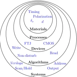
digital memory applications, specifically focusing on device performance/optimization and system enablement. It explores material properties, basic device performance, process development for CMOS integration, and related system design including sim-ulated performance. By optimizing material properties of its various parts, the device can exhibit a range of performance from ultra low power with large memory window to low power with better speed performance when implemented with address systems (lower τ = RC). This research work thereby endeavors to provide a full founda-tion, see Figure 1.1, for further exploration and fabrication of HfO2-based FTJ, both
specifically at RIT and (with process modifications for varying CMOS device types and sizes) at any facility.
1.2
Thesis organization
CHAPTER 1. INTRODUCTION
Timing
Polarization
δx d
Materials
Processes
FTJ CMOS
Devices
Write
Read Non-disturb
Algorithms
Veriloga Address
Scan/Hold Output
[image:19.612.200.450.70.321.2]Systems
Figure 1.1: Diagram representation of the dependencies of various implementation stages of the technology presented in this thesis.
properties of ferroelectric materials and highlights some specific aspects which are of concern to their implementation in FTJs. Chapter 3 reviews the history of ferro-electric memories, the discovery and subsequent explanation of FTJs, and the ideal applications of these devices while also presenting alternative technologies and com-paring their performance. After demonstrating the advantages of FTJs, Chapter 4 presents simulation (from quantum-mechanical basis) of device operation, with corre-sponding band structures and current densities in each memory state (using a custom python script). Finally, an FTJ using ferroelectric HfO2 is designed and simulated in
Chapter 5 and its performance is compared to other state of the art FTJs. In this same chapter, a CMOS-integrated fabrication process for HfO2-based FTJ devices
pre-sented. This work therefore provides a nearly comprehensive overview of FTJ devices from materials to systems, including ferroelectric HfO2 device simulation, the design
of a full CMOS-integrated fabrication process, and Cadence Virtuoso system design and simulation with custom Verilog-A behavioral analog models of designed FTJs.
1.3
Neuromorphic Computing with Memristors, ReRAM
Neuromorphic systems with ReRAM as synapse elements have been reported which take advantage of the intrinsic similarity between such devices and synapses (both are two-terminal and behave memristively). ReRAM devices inherently pass more cur-rent as they are programmed further (provided they can be so-designed) and therefore provide both space-reduction (compared to larger CMOS elements or register imple-mentation) and simplification of STDP response generation. In their papers, Ambro-gio et. al report low-power (≈105 power reduction) generation of STDP signals with
ReRAM 1 transistor - 1 resistor (1T1R) synapse elements constituting a neuromor-phic system capable of unsupervised learning of MNIST handwritten digits achieving 86% accuracy [17]. Further, the power consumption of the system was reduced to 1×10⁻¹² Joules per neuron event, using a series of short pulses for write/read, and
enable ultra-low power computation [18]. Park et. al used TiOx-based ReRAM in
CHAPTER 1. INTRODUCTION
1.4
Using Ferroelectric Tunnel Junctions
An FTJ is very similar to a ReRAM device in function (both two terminal mem-ristors), but differs in mechanism. Where ReRAM elements are either filamentary (create/break a mechanical filament on program/erase) or non-filamentary (often in-volving changing concentration of oxygen vacancies at the barrier interface) [20], a change in resistance for an FTJ is based on the changing internal polarization field magnitude and direction of a ferroelectric material separated by two electrodes of dif-ferent materials (specifically having differing Debye lengths) [4]. Since, optimally, a synaptic element will have a smooth (analog) transition from having seen no potenti-ation (and little response) to many recent potentipotenti-ations (and large response), an FTJ for such application should include a ferroelectric material with as many domains as possible and a low coercive electric field such that the ferroelectric depolarizes under the absence of repeated stimuli. Such a film will be slightly thicker than typical for FTJ used in non-volatile memory (NVM) and of a larger area. These properties are in contrast to those required for NVM (high coercive field and low # of polarization do-mains). Ferroelectric HfO2 is a good candidate due to the large difference in resistive
states possible,the ability to get a large number of domains in even small areas, and high speed performance with write/read times of 10 ns [21]. Interestingly, HfO2-based
Physics of Ferroelectric Materials
Ferromagnetism (permanent magnetic moment) was the first ferroic property dis-covered and was so-named because it occurs often in iron-containing alloys. Ferro-electricity is a property of materials which exhibit spontaneous electric polarization (dipole moment density) and although most ferroelectrics do not contain iron, was so-named because of it’s relation to the other ferroics (materials which can polarize in some way) and was classified as such. In a basic sense, a ferroelectric is a dielectric that (once stimulated) exhibits a non-zero reversible polarization at 0 applied electric field, as shown in Figure 2.1. This remanent polarization, Pr, is due to an internal
potential, covered in more detail in the next few sections. Most ferroelectrics are ei-ther transition metal oxides or chalcogenides. Additionally, materials can exhibit any ferroic property independent of the others, and will also always be piezoelectric, and a material which exhibits any two or more (excluding piezoelectricity) is considered ”multiferroic” [22].
2.1
Crystal structure
CHAPTER 2. PHYSICS OF FERROELECTRIC MATERIALS
Figure 2.1: Ferroelectric polarization (a) and weak magnetic moment (b) of multiferroic Bi2NiMnO6 at 7K, from Shimakawa et. al [1]. The red line on (a) is what this plot would look like for a perfect dielectric.
T
>
T
c-+
+
+
T
<
T
cand
←−−
E
app-+
+
+
T
<
T
cand
−−→
E
app-+
+
+
Figure 2.2: Simple representation of the atomic structures of a ferroelectric as its prototype phase (left) relaxes into one of two polar phases (middle and right) after the application of an external field. A ferroelectric would remain in the corresponding state even after the removal ofEapp, while a dielectric would deflect (as shown) during stimulus application but relax to the non-polar phase (left) once that field was removed.
represented in Figure 2.2, and exhibits an aggregate total polarization field based on the orientation of domains (as a function of defects and grain boundaries). This topic (and more complicated derivations of the physical phenomena of ferroelectrics) is explored more completely in the famous book by Lines and Glass [22].
2.2
Polarization in ferroelectrics and dielectrics
[image:23.612.125.526.300.396.2]atom to remain in that position (along an arbitrary plane) follows a quadratic curve with only one minimum at the zero-field position. This is because a simple dielec-tric has a centrosymmedielec-tric crystal structure. A similar plot of atomic energy versus position in a ferroelectric unit cell would instead behave as (x2+a)(x2+b) +c and
exhibit two separate minimas. This is because the crystal structure of a ferroelectric is non-centrosymmetric, and is the physical origin of the macroscopic polarizability of a ferroelectric film [22]. Furthermore, the polarization at zero applied field is called remanent polarization, Pr. It can be either expressed in each polarization state
(pos-itive Pr,+ or negative Pr,−) or as the total of both states 2Pr = Pr,+ +Pr,− (often
in the case of symmetric states, where Pr,+ = −Pr,−). The electric field required
to transition from one polarization state to the other (where P passes through 0) is called the coercive electric field, Ec=Vc/d [22]. Figure 2.1 shows a ferroelectric film
with 2Pr = 8µC/cm2 and Ec= 0.1 MV/cm.
2.3
Non-intrinsic ferroelectrics
Though most ferroelectrics were classically demonstrated as bulk materials and later implemented as thin films, recent improvements in film deposition technologies have enabled the engineering of materials which could be called ”non-intrinsic” ferro-electrics. Typically, the crystallization of a material proceeds in an effort to min-imize total energy and occurs unconstrained (meaning the atoms are free to move within the lattice). Recently, a group from NamLAB deposited films of HfO2 by
atomic layer deposition (ALD) and incorporated varying atomic % of Si atoms. After annealing, unconstrained, the material crystallizes to a mixture of typical monoclin-ic/tetragonal phases (which are centrosymmetric). However, by capping the HfO2
with a thin film of TiN and annealing at a temperature such that the TiN atoms were likely still in a stable form, the HfO2 crystallizes to orthorhombic phase and is
CHAPTER 2. PHYSICS OF FERROELECTRIC MATERIALS
[image:25.612.169.479.69.130.2]↑
←
↓
→
↓
Figure 2.3: Simple diagram of domains in a model ferroelectric film.
of the atomic stress from Si doping, the extra strain energy introduced by the cap-ping material, and the inhibition of relaxation modes available when un-capped. The Ferroelectric Device Research at RIT (FeDR RIT) group, working with NaMLAB, have successfully demonstrated similar material results at RIT by doping HfO2 with
Al, using similar capping and anneal strategies.
2.4
Ferroelectric domains
A realistic ferroelectric film will not be perfectly oriented all the same direction, as considered in Figure 2.2, but instead have many differently oriented crystal clusters, due to defects. A very basic visualization of this effect is shown in Figure 2.3, and is explored more thoroughly in the book by Lines and Glass [22]. In general, the maximum size of a domain can be extracted based on crystal parameters but for most materials is roughly 20 to 100 nm.
2.5
Area-dependent effects
The response of an FTJ can be affected by the domains which exist in the ferroelectric, with reference to the area of the device. Consider, if the maximum domain size is close to the area of FTJ devices, some devices will encompass only one domain which is oriented parallel to the applied field. These devices would have maximum performance, since the entire film contributes to polarization (Pmax). However, this
Chapter 3
Brief History and Applications of FTJ Implementations
3.1
Early memory using large-dimension PZT
Though not FTJs, ferroelectric memories were first reported in an MIT masters thesis by Dudley Allen Buck in 1952 [24]. Larger ferroelectric memory arrarys by Bell Labs were also discussed in a Scientific American article in 1955 by Ridenour [25] though a good explanation of such devices was not given until a 1973 IEEE article by Kaufman [2]. These ”bender memory” devices used 5 mil (127 µm) thick PZT ferroelectric films sandwiched between conducting electrodes, shown in Figure 3.1, to store data in polarization which creates a positive or negative pulse (while clamped, due to the electrostrictive and piezoelectric response) in response to application of a read voltage. These devices were very high power (30 V/mil write, 45V read) and very slow (≈ 1 ms) [2].
3.2
More recent implementations with BaTiO
3As covered briefly in Section 4.2, Contreras et. al discovered the first FTJ using BaTiO3, a ferroelectric well known since it’s initial synthesis as a bulk material. In
that paper, the group had investigated both Pt/PZT/SrRuO3and SrRuO3/BaTiO3/SrRuO3
-Figure 3.1: ”Bender memory” schematic from [2]. This 8-bit device stores data as re-manent polarization in the top-most ferroelectric material. Write pulse is ≈1 ms of 20-30 V/mil.
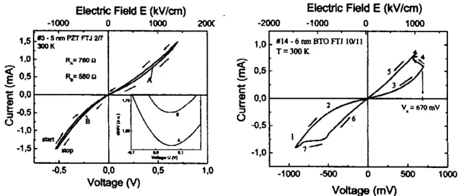
based FTJ had a memory window of HRS/LRS ≈ 3, shown in Figure 3.2 [3]. As already discussed in Section 4.2, the memory window is heavily dependent on the dissimilarity of screening lengths between electrodes and, considering this FTJ has the same material for both electrodes, it’s surprising that the performance is so good. The group (Contreras, Kohlstedt, et. al) clears up this incongruity in their 2005 paper where, in addition to using the findings of Zhuravlev et. al [4] to explain FTJ per-formance, they report that the interface between bottom electrode and ferroelectric exhibits a Ruddelsen-Popper interfacial layer which modifies the effective screening length for that electrode, increasing asymmetry and therefore memory window [26].
Groups have continued to research BaTiO3-based FTJs, including a recent 2013
paper by Wang et. al which presents a device with Co and La0.67Sr0.33MnO3 as
electrodes. The group achieves a memory window HRS/LRS ≈ 100 with a 2 nm ferroelectric and demonstrates switching times as fast as 13 ns (for relatively high write voltages, ≈ 3Vc). They also use extracted values to design a Verilog-A model
[image:28.612.206.443.78.261.2]CHAPTER 3. BRIEF HISTORY AND APPLICATIONS OF FTJ IMPLEMENTATIONS
Figure 3.2: Performance of FTJs for (a) fresh device with PZT ferroelectric and (b) device with BaTiO3 ferroelectric after -1.2V priming pulse, taken from Contreras et. al [3].
3.3
Applications of FTJs
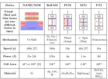
FTJ devices are ideal for two main applications; non-volatile digital memory and brain-inspired computing. Portable electronics demand fast, low-power storage de-vices and, as shown in Table 3.1, FTJ provide the highest speed and lowest power.
Device NAND/NOR ReRAM PCM MTJ FTJ Visual (Red and blue boxes are two different states in time)
n+-PolySi Control Gate SiO2Barrier Oxide
n+-PolySi Floating Gate SiO2Tunnel Oxide
n+S/D n+S/D
p−-Si Substrate
[image:30.612.146.505.64.325.2]M1 ... ... ... ... ... ... ... ... ... .... ... ... M2 M1 M2 M1 → ← ← ← M2 M1 ↑ ↓ M2
Mechanism Vt Shift
O2Vac./
Filamen-tary
Phase change
e− Spin
(Mag) Polarization
Speed (s) 400u [27] 500n 50n 30n [27] 10n
Power (J) 15u [28] 250n 6p 1.4u 30f
Cell Area 4F2or 10F2[29] 25F2 16F2 1.3F2 22F2
Material Si Ag, a-Si,
W Ge2Sb2Te5 MgO(mag)
BaTiO2
(now HfO2)
Table 3.1: Performance of alternative technologies compiled from various sources. MTJ values from Aziz et. al and Lee et. al. [5, 6], all other from Ebong et. al. and Kim [7, 8] unless otherwise referenced in table.
and non-volatile memory applications.
3.4
Alternative technologies
Memristors can be implemented by a few different technologies, each with their own characteristic strengths and shortcomings, which are discussed in this section.
3.4.1 Filamentary ReRAM
CHAPTER 3. BRIEF HISTORY AND APPLICATIONS OF FTJ IMPLEMENTATIONS
Neuron
[image:31.612.159.502.72.205.2]Synapse CMOS NeuronMemristor
Figure 3.3: Simple diagram of (left) a physical model of neurons and synapses, the brain’s computation devices, and (right) their electronic implementation in a typical brain-inspired computing system.
are well-understood and widely used, they are not very low power (3.5V program pulses applied to devices with Ravg ≈1MΩ) and are rather slow (≈100 µs program
times, ≈500 µs read) [32].
3.4.2 Magnetic tunnel junctions
The MTJ is designed as a tunnel oxide sandwiched between two ferromagnetic ma-terials. One of the ferromagnets is pinned to be magnetized in a direction, while the other is free to magnetize parallel or anti-parallel to it (controlled by inducing a magnetic field in it by passing a large current through a nearby conducting material). When both magnetic films are oriented parallel the tunnel resistance through the de-vice is lower than when anti-parallel (due to the effect of spin-transfer torque). These devices can achieve memory windows as high asHRS/LRS ≈1000, but usually have higher current density in both states than FTJs and also require rather large current pulses to write the magnetic state [5, 6].
3.4.3 Phase-change memory
Chapter 4
Analysis of M1-Fe-M2 Structure
At its core, an FTJ is a modified MIM so it’s logical to start by examining an MIM and modifying our analysis to reflect the different material properties. All band structure and current density figures in this section, except Figure 4.3, are simulated results performed in this work using a custom python program included in Appendix A.
4.1
Band structure in the absence of polarization field
An MIM with non-ferroelectric insulator has no internal polarization field and there-fore returns to the same zero-field band structure, shown in Figure 4.1, after any external field application (for d = 2 nm thick insulator with Ea = 2 eV and metals
havingχ1 = 4.08 eV,χ2 = 4.85 eV). The thermionic emission current, from electrons
which gain sufficient energy from phonon interaction to surmount the barrier, of such a device is calculated using Equation 4.1, and for our example is roughly 1e-41 A/cm2 (practically ”0” current) at 0.5V. Since this MIM has an insulator with thickness less than the penetration distance of the electron wave, an appreciable current occurs due to Fowler-Nordheim tunneling,Jtun, when electrons are able to quantum-mechanically
tunnel through the triangular or trapezoidal energy barrier. This current, calculated using Equation 4.2, is shown in Figure 4.2 and is the main current contributing mech-anism for this type of device (7e4 A/cm2 at 0.5V for this example). Like most MIMs,
where the current becomes ”zero” and also has a slight asymmetry between curves under negative and positive applied voltage.
−6 −4 −2 0 2 4 6 8
0 0.5 1 1.5 2 2.5 3
M1
I
M2
(χ1−Ea) (χ2−Ea)
Position (nm) P oten ti al ab o v e EF (eV)
[image:34.612.131.518.128.376.2]Band diagram of an MIM
Figure 4.1: The energy band diagram of an MIM with a 2 nm thick insulator withEa= 2 eV and metals havingχ1 = 4.08 eV,χ2 = 4.85 eV, normalized to the fermi energy.
Jth=AthT2exp(−ψ0/kBT)(1−exp(−qV /kBT))
where, Ath=
4πm∗qk2
B h3
(4.1)
Jtun=J0
¯
ψexp
−Atun
q
¯
ψ
−( ¯ψ+qV) exp
−Atun
q
¯
ψ+qV
J0=
q
2πh(βd)2 ψ¯= 1
d d
Z
0
ψ(x)dx, is mean barrier height
Atun=
4πβd√2m∗
h β is a correction factor, usually 1
(4.2)
4.2
Band structure under polarization
When the first FTJ was discovered by Contreras et. al in 2002, BaTiO3 ferroelectric
origi-CHAPTER 4. ANALYSIS OF M1-FE-M2 STRUCTURE
−1 −0.8 −0.6 −0.4 −0.2 0 0.2 0.4 0.6 0.8 1 102
103
104 105
Applied voltage, V (V)
Absolute
curren
t
densit
y
(
|
A
|
/
cm
2 )
[image:35.612.126.522.75.324.2]Current density versus applied voltage
Figure 4.2: The Fowler-Nordheim tunneling current of an MIM with material properties listed in Section 4.1.
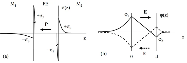
nally published purely as a dissemination of experimental results. [3] It was not until 2005 that the phenomenon was explained by Zhuravlev et. al, who postulated that the ferroelectric polarization, P, induces equal and opposite surface charge densities, σp =−P, which exist in infinitessimally thin sheets at the interfaces of each contact
and the ferroelectric. Shown in Figure 4.3, the surface charges must then be locally screened by each electrode, thereby inducing screening charge densities, σs, as given
by Equation 4.3, with screening lengths (or debye lengths) in metal 1, σ1, and metal
2,σ2, given by Equation 4.4. Finally, these charges modify the zero-polarization band
structure with additional potentials within both electrodes and the ferroelectric, as given by Equation 4.5 and shown in Figure 4.3 by Zhuravlev et. al [4]. Though not explicitly given by the group, it is clear that the additional potential contribution within the ferroelectric is given by Equation 4.6.
σs=
P d εf(δ1+δ2) +d
Figure 4.3: (a) Diagram of charge densities created for left polarized ferroelectric and (b) corresponding generated potentials across an FTJ, having electrodes with dissimilar screening lengths, from Zhuravlev et. al [4].
δx =LD =
s εkBT
q2N x
where, for a metal Nx =c0 (4.4)
ψ(x) =
σsδ1exp(−|x|/δ1)
ε0
, x≤0
−σsδ2exp(−|x−d|/δ2) ε0
, d≤x
(4.5)
ψ(x) =
ψ(0) + (ψ(d)−ψ(0))x d
, 0< x < d (4.6)
It’s clear to see already that for electrodes with dissimilar screening lengths there will be a non-zero depolarizing field, because of the reduced field contribution from charges further from the interface, and there will be a difference in average potential barriers for polarization towards M1 versus M2. Finally, integrating all the above contributions from polarization-induced charges to the zero-field band structure, an FTJ with material properties consistent with those used in Section 4.1 (and assuming P = 10µ C/cm2, ε
f = 40ε0, δ1 = 0.06 nm, and δ2 = 0.4 nm) would exhibit band
CHAPTER 4. ANALYSIS OF M1-FE-M2 STRUCTURE
−6 −4 −2 0 2 4 6 8
0 0.5 1 1.5 2 2.5 3 3.5
M1
I
M2
Position (nm)
P
oten
ti
al
ab
o
v
e
EF
(eV)
Band diagram of an FTJ
[image:37.612.129.518.76.321.2]P=+P P=-P
Figure 4.4: The energy band diagrams, at V = 0, of an FTJ with material properties given in Section 4.2, for positive (towards M1) and negative (towards M2) polarization.
4.3
Extraction of tunnel Current and (by extension)
resis-tance states
The tunnel current density for each state (positive polarization and negative polariza-tion), is calculated again using Equation 4.2, but now requires the additional potential contributions of equations 4.5 and 4.6. For this case, positive polarization (towards M1) has a lower barrier than negative polarization (towards M2), so we will term each state the LRS and HRS, respectively. The corresponding current density curves are shown in Figure 4.5, and is representative of an FTJ having Al as M1, Al:HfO2
as ferroelectric, and degenerately doped (Na = 1×1020 cm−3) p+ Si as M2. Since
the resistivity is given by ρ=E/J =V /(dJ), the resistance states would correspond directly to the current densities of each state. Lastly, the memory window is a ratio of the device’s resistivity (at the same applied voltage, usually the read voltage,vdda)
−1 −0.8 −0.6 −0.4 −0.2 0 0.2 0.4 0.6 0.8 1 102
103 104 105
Applied voltage, V (V)
Absolute
curren
t
densit
y
(
|
A
|
/
cm
2 )
Current density versus applied voltage
[image:38.612.129.521.255.501.2]LRS HRS
Chapter 5
Design of Ferroelectric HfO
2-based FTJs and Integration
with CMOS Process
For this design, a twin-well polysilicon-gate planar CMOS process flow by Lynn Fuller [34] was modified by the addition of required steps for deposition and patterning of the ferroelectric. If being fabricated at RIT, the author recommends keeping designed CMOS devices at a minimum length of 2µm to achieve highest yield, though adaptation of these processes to another process with smaller minimum feature size and varying gate material would be relatively straight-forward.
5.1
FTJ design
In an effort to keep the FTJ fully CMOS-compatible the electrodes were chosen to be Al and p- doped Si, as shown to be effective in Section 4.3. Each device is designed as a crossbar such that the area of an FTJ is the width of the p- electrode times the width of the Al electrode. This way, a larger array of FTJ devices are designed as horizontal p- lines (in ”oxide” mask level) and vertical Al lines.
In order to predict and optimize FTJ performance, all equations from Section 4 were integrated into a flexible python program with user-interface for input of relevant material properties. The code for this program is given in Appendix A.
0 10 20 30 40 50 60 70 80 90 0
5 10 15
δ2 δ1
HRS/LRS
[image:40.612.123.522.72.295.2]Memory window versus screening length ratio, δ1 = 0.5 ˚A
Figure 5.1: Simulated HRS/LRS increases with larger screening length ratio before plateauing around δ2
δ1 ≈60. For an Al/Al:HfO2/p+ Si FTJ with 2 nm ferroelectric.
0.5 ˚A), as shown in Figure 5.1, shows a saturation starting at around 60 ≈ δ2/δ1
(corresponding to δ2 = 3 nm, p+ Si Na = 2×1018 cm−3).
Even more interestingly, varying the screening length in the ”good” metal (while keeping the poor metal δ2 = 3 nm), as shown in figure 5.2, yields two important
conclusions. First, a metal with incredibly high carrier concentration (δ1 < 0.05˚A)
would actually cause a sharp decay in memory window, owing likely to the total screening of the depolarizing field at that interface and (by extension) a removal of its positive effect on introducing dissimilar barriers. Second, the memory window improves with increased screening length but reaches a maximum at δ1/δ2 ≈ 0.38.
CHAPTER 5. DESIGN OF FERROELECTRIC HFO2-BASED FTJs AND
INTEGRATION WITH CMOS PROCESS
0 0.1 0.2 0.3 0.4 0.5 0.6 0.7
0 10 20 30 40
δ1 δ2
HRS/LRS
[image:41.612.126.522.106.328.2]Memory window versus screening length ratio, δ2 = 3 nm
Figure 5.2: Simulated HRS/LRS for increasing δ1, showing a maximum. For an Al/Al:HfO2/p+ Si FTJ with 2 nm ferroelectric.
2 3 4 5 6 7 8 9 10 11
101 103
105
107
Ferroelectric Thickness (nm)
HRS/LRS
10−4 101
106
1011
1016
ρHRS
(Ω
·
cm
2
at
V
=
0
.
1
V)
Max Current Ratio HRS Resistivity
[image:41.612.126.527.441.647.2]5.2
State of the art FTJs
For this study, it is best to assume the Al electrode will behave non-optimally (having no impurities) and therefore, the FTJ design for the Al/Al:HfO2/p-Si device presented
in this work has material properties δ1 = 0.06 nm, χ1 = 4.08 eV, εf = 40ε0, Ea = 2
eV, Pr = 15µC/cm2, d= 2,3, or 5, m∗ = 0.11me,δ2 = 3 nm, and χ2 = 4.85 eV. The
Al:HfO2 ferroelectric is adapted from the process used by Polakowski et. Al [35] and
is assumed to behave with similar speed, polarization, and endurance performance. A comparison of this device to other state of the art FTJs is shown in Table 5.1. Importantly, the small coercive electric field (Ec) of HfO2-based ferroelectrics leads to
a lower required program voltage (the coercive voltage,Vc), and therefore lower power
consumption, compared to BaTiO3 and BiFeO3 FTJs. Speed performance between
FTJs are mostly similar, though endurance of HfO2-based devices is higher than
that of BiFeO3 devices. Most importantly, the Al/Al:HfO2/p-Si FTJ can be designed
with either a 2, 3, or 5 nm ferroelectric layer; leading to performance with either lower high-state resistivity (ρHRS) than all other FTJs (enabling high speed performance
by minimizing τ = RC) while only exhibiting moderate power density (Pd) with a 2 nm ferroelectric or very high ρHRS with a potentially huge memory window of
5×10⁵ and extremely low power performance (2.5 fJ for each 500 nm2 device) with a
5 nm ferroelectric (more ideal for NMC applications where a large memory window permits more memory states). At a more moderate performance optimization, a 3 nm ferroelectric in the Al/Al:HfO2/p-Si FTJ yields a memory window similar to
that of the BaTiO3 FTJ reported by Abuwasib et. Al [9] but achieves lower power
consumption by a factor of ≈1×10⁻³. All three of these simulation results indicate
that Al:HfO2-based FTJs are superior to both alternative technologies and FTJs using
CHAPTER 5. DESIGN OF FERROELECTRIC HFO2-BASED FTJs AND
INTEGRATION WITH CMOS PROCESS
Researcher [cite] Device Materials Ec (V/cm) Area CMOS?
Chanthbouala et. Al [36] FTJ Co/BaTiO3/LSMO 1×10⁷ 0.096 No Abuwasib et. Al [9] FTJ Co/BaTiO3/LSMO 1×10⁷ 0.303 No Boyn et. Al [12] FTJ Co/BiFeO3/CCMO 3.3×10⁶ 0.125 No Mueller, Schroeder et. Al [37, 38] MIM Pt/TiN/Si-HfO2/TiN 1×10⁵ 10000 Yes Polakowski et. Al [35] MIM TiN/Al:HfO2/TiN 1×10⁵ 50 Yes This Work (Based on Simulations) FTJ Al/Al:HfO2/p-Si 1×10⁵ 0.25 Yes
Research d(nm) ρHRS (Ω·cm2) HRS/LRS Pr Speed Endurance Vc Pd (W/cm2)
[36] 2 4.8×10⁻² 300 - 10 ns - 2.0 83.3
[9] 2 4.8×10⁻³ 60 - - - 2.0 823
[image:43.612.109.566.186.298.2][12] 4.6 5×10⁻² 1000 100 100 ns 4×10⁶ 1.5 45
[37, 38] 10 - - 17 10 ns 1×10¹⁰ 1.0
[35] 12 - - 15 not rep. 2×10⁹ 1.2
This Work
2 1.8×10⁻⁴ 6.2
15 10 ns 2×10⁹
0.2 222
3 1.54×10⁻¹ 90 0.3 0.584
5 2.3×10⁵ 500000 0.5 1×10⁻⁶
5.3
Designed CMOS-process with FTJ-fabrication steps
Step Num b er Step Co de Step Description T o ol Time (hrs) 1 O X05 pad o xide 500 ˚ A, T ub e 4, 45 min at 1000C Bruce F urnace 4 3 2 CV02 1500 ˚ ASi3N4 LPCVD Dep osition, 30 min at 810C LPCVD Nitride 4 3 PH03 lev el 1-Oxide -Clear Field ASML & SS I 1 4 ET29 Plasma etc h Nitride, 1500˚ Atarget
LAM 490 0.3 5 ET07 ash all photoresist Gasonics Asher 0.15 6 CL01 R CA clean R CA Benc h 0.85 7 O X04 First Oxide T ub e 1, 3650 ˚ ABruce 1 Recip e 330, 55 mins at 1000C Bruce F urnace 1 2.65 8 ET06 Etc h O xide, 3650
˚ Atarget,
CHAPTER 5. DESIGN OF FERROELECTRIC HFO2-BASED FTJs AND
INTEGRATION WITH CMOS PROCESS
Step Num b er Step Co de Step Description T o ol Time (hrs) 19 IM01 NMOS Vt, 7.95e12, P31, 60KeV V arian Implan ter 6 20 ET07 ash all photoresist Gasonics Asher 0.15 21 PH03 lev el 5 – PMOS VT adjust -n w ell lev el -dark field ASML & SS I 1 22 IM01 PMOS Vt, 3.02e12, B11, 30 KeV V arian Implan ter 6 23 ET07 ash all photoresist Gasonics Asher 0.15 24 ET06 etc h 500 ˚ A pad o xide, 50:1 H2 O:HF (3.6 mins) 50:1 HF Etc h 0.25 25 CL01 pre-gate o xide R CA clean (with extra e tc h, next step) R CA Benc h 0.85 26 ET06 etc h nativ e o xide (extra 30s 50:1 HF dip) R CA Benc h 0.1 27 O X06 100 ˚ A dry (N 2 O) gate o xide, Bruce T ub e 4, Recip e 213, 60 mins at 900C Bruce F urnace 4 3 28 CV01 LPCVD p oly dep osition, 4000 ˚ A LPCVD P olysilicon 4 29 PH03 lev el 6 – p oly gate -clear field ASML & SS I 1 30 ET08 p oly gate plasma etc h, 4000
˚ Atarget,
Step Num b er Step Co de Step Description T o ol Time (hrs) 37 PH03 lev el 8 – n-LDD -dark field ASML & SS I 1 38 IM01 PMOS LDD, 4E 13, P31, 60 KeV V arian Implan ter 4 39 ET07 ash all photoresist Gasonics Asher 0.15 40 CL01 R CA clean R CA Benc h 0.85 41 CV02 LPCVD nitride spacer 3500 ˚ A LPCVD Nitride 4 42 ET39 sidew all spacer etc h, 3500
˚ Atarget,
CHAPTER 5. DESIGN OF FERROELECTRIC HFO2-BASED FTJs AND
INTEGRATION WITH CMOS PROCESS
Step Num b er Step Co de Step Description T o ol Time (hrs) 52 ME03 HF dip & Ti Sputter CV C601 3 53 R T01 R TP 1 min, 650C R TP 1 54 ET11 Unreacted Ti Etc h Etc h Benc h 1 55 R T02 R TP 1 min,800C R TP 1 56 CV03 TEOS, P-5000, 4000
˚ AOxide
CHAPTER 5. DESIGN OF FERROELECTRIC HFO2-BASED FTJs AND
INTEGRATION WITH CMOS PROCESS
Step Num b er Step Co de Step Description T o ol Time (hrs) 75 ET07 ash all photoresist Gasonics As h e r 0.15 76 CV03 TEOS, P-5000, 4000
˚ AOxide
P5000 TEOS Ch A 0.5 77 PH03 Via1 -dark field ASML & SSI 1 78 ET26 Via Etc h Drytek Quad 0.5 79 ME01 Al Dep osition CV C601 1 80 PH03 Metal 2 -clear field ASML & SSI 1 81 ET15 plasma 125W, Al Etc h, BC l, Cl2, Chloroform, T arget 7500 ˚ A LAM4600 1.5 82 ET07 ash all photoresist Gasonics As h e r 0.15 83 CV03 TEOS, P-5000, 4000
˚ AOxide
Step Num b er Step Co de Step Description T o ol Time (hrs) 86 ME01 Al Dep osition CV C601 1 87 PH03 Metal 3 -clear field ASML & SSI 1 88 ET15 plasma 125W, Al Etc h, BC l, Cl2, Chloroform, T arget 7500 ˚ A LAM4600 1.5 89 ET07 ash all photor e sist Gasonics As h e r 0.15 90 CV03 TEOS, P-5000, 4000
˚ AOxide
CHAPTER 5. DESIGN OF FERROELECTRIC HFO2-BASED FTJs AND
INTEGRATION WITH CMOS PROCESS
To minimize additional process steps, the p-Si electrode is defined by the pseudo-STI field oxide growth (steps 3-9) which also defines the active areas of transistors. This process does exhibit some feature thinning, so a 2 µm line on mask (transferred to nitride) yields approximately a 250 nm line width of exposed silicon for the elec-trode. The p- doping is introduced during the implant for PMOS-device source/drain, step 47. A modified version of step 47, called step 47(2), can be used to study the affect of n-doping instead of p-doping the lower (M2) electrode, but cannot be used with full CMOS integration. To confine Al:HfO2 to FTJ areas, the same tetra-ethyl
orthosilicate (TEOS) oxide used as an interlevel dielectric (ILD) below each metal layer is deposited, step 56, and patterned, step 57, to open windows to FTJ areas before Al:HfO2 deposition by ALD, step 60. The Al:HfO2 is also capped in-situ with
TiN before being annealed in RTP (to form the ferroelectric state), step 61. The TiN must then be removed, since it is conducting and would cause device shorts, and is selectively removed, in step 63, by the SC1 chemistry used in a standard RCA clean (at a rate of 1nm/s), as shown by Liu et. al [39]. This must be done in a pyrex dish on a hot plate in a wet etch bench, not in the RCA bench, to avoid contamina-tion. Finally, the same mask used to open windows in the TEOS can be used with negative resist, in step 65, to create a soft mask protecting the FTJ areas and then etch the Al:HfO2, in step 66, from unwanted areas (though this is not necessary).
Figure 5.4: Athena simulation of CMOS devices tuned for low threshold voltages (left) and FTJ device (right).
5.4
Process simulation
Silvaco is a semiconductor simulation tool used often in both academic and industry research. It has modules for process simulation, Athena, and electrical simulation of a simulated process,Atlas; though electrical simulations are more suited to transistor performance and related connections. In order to verify the proposed process design, from Section 5.3, it was simulated usingAthena. The code is included in Appendix C and important figures are shown in this section. Importantly, the CMOS devices are shown in Figure 5.4, showing appropriate wells and junction depths for source/drain. The window opened in TEOS is shown to be appropriate for isolating ferroelectric to desired areas, shown in Figure 5.5 with SiO2 substituted for HfO2 since Athena does
not have it. This simulation platform was also used to fine tune the use of wet etch before HfO2 deposition to accurately reach 250 nm device width, shown in Figure 5.6.
CHAPTER 5. DESIGN OF FERROELECTRIC HFO2-BASED FTJs AND
[image:53.612.151.497.124.318.2]INTEGRATION WITH CMOS PROCESS
Figure 5.5: Athena simulation of FTJ device (SiO2 substitued for ferroelectric).
[image:53.612.151.498.450.646.2]System Design and Simulations for Digital Memory
Applications
The designs of all circuits were performed inCadence Virtuoso using a 45 nm CMOS PDK. The design rules of this PDK are consistent with those required for the 2 um process to be performed at RIT but allowed for easier use of the DRC and LVS tools native to this PDK. Additionally, this allowed for performance simulation represen-tative of implementation with fairly modern devices. When implemented in the 2 um CMOS process at RIT, the mask file from Virtuoso was simply scaled up (from 45 nm to 2 um, a factor of 44.44) before mask printing.
6.1
Read/Write scheme
When writing an FTJ, the bias applied across it must meet or exceed the coercive voltage, Vc, in order to flip the polarization to the desired direction (over any
rea-sonable amount of time). While reading, the bias must be less than Vc in order to
prevent state disturbance. Let’s take, for example, an FTJ withVc = 0.5 V. As shown
in Figure 6.1, these schemes would work to write the HRS and LRS as shown and to read the device (since read will always be performed in the same direction).
CHAPTER 6. SYSTEM DESIGN AND SIMULATIONS FOR DIGITAL MEMORY APPLICATIONS
p n
V=0.6V V=0V
Write HRS
p n
V=0V V=0.6V
Write LRS
p n
V=0.4V V=0V
[image:55.612.166.505.68.163.2]Read
Figure 6.1: An address scheme which, though appropriate for a stand-alone device, would be inappropriate for devices in an array.
p
n
p
n
p
n p
n
Figure 6.2: A simple schematic showing the typical connectivity of FTJ devices in an array, for both memory or neuromorphic logic applications. Lines and columns only connect through FTJ devices and do not connect at intersections. Dotted lines indicate an arbitrary number of repeated lines and columns.
other non-addressed devices in that row or column would experience the same bias as the addressed device!
Ultimately, the best solution to this will be one of two options and will be up to the system designer. The first option is to have rails centered around ground such that the write rails are (for our example)VDD=0.3 V andVSS=-0.3 V, read rails arevdda=0.2V
and vssa=-0.2V and whenever a column or row is not being addressed it should be
[image:55.612.210.441.207.437.2]p n
V=0.3V V=-0.3V
Write HRS
p n
V=-0.3V V=0.3V
Write LRS
p n
V=0.2V V=-0.2V
Read
Figure 6.3: An address scheme appropriate for FTJs in an array.
p n
V=0.3V V=0V
Write HRS
p n
V=-0.3V V=0V
Write LRS
p n
V=0.2V V=0V
Read
Figure 6.4: addressed devices in the same row, for various write/read states. Non-addressed devices in the same column would experience the opposite bias. In this way, these devices will not be disturbed.
read or write.
Though this address choice does allow non-addressed devices to stay at ground, preventing current flow through the FTJ devices to the bulk silicon (which is typically grounded) it does require CMOS devices with near-zero threshold voltage. If this is undesirable, another option is to shift all rails by +VDD, leaving the write rail low
at 0V but requiring all non-addressed lines to be held (for our example) at 0.3V. Ultimately, this is the decision of the system designer and depends on related process constraints.
6.2
Linear resistance change simulation
CHAPTER 6. SYSTEM DESIGN AND SIMULATIONS FOR DIGITAL MEMORY APPLICATIONS
state and saturate once reaching the resistance of that state. Simulation results using CMOS devices from the 45nm PDK of Cadence Virtuoso (used for ease of DRC and LVS, and for results more representative of a modern CMOS process) are shown in Figure 6.10 and are useful for digital memory applications, with write times of ≈0.6 ns for HRS and ≈0.3 ns for LRS and read times of ≈10 ns for HRS and ≈4 ns for LRS. However, brain-inspired computing systems, which require precise control as the device transitions from one state to the other, need a more complicated simulation which models polarization change versus time and corresponding resistance.
6.3
Timing-based simulation
Working with data for polarization versus program time from Schroeder et. al [41], piece-wise polynomial models were fit to the data and used to direct further study of the general phenomena of timing in ferroelectrics. Some modeled curves are given in Figure 6.5 and the equation and relevant model fit parameters are given by Equation 6.1. Though these curves suggest switching times close to 1 µs, the group posits that this data was influenced by the test setup delay and that realistic switching times are in the 1 ns range [41].
2P r(V, t) = M IN
M IN(13.071∗V2.929,6.339∗V + 27.357)
, M AX(M IN(D+E∗ln(t), M AX(A+Blog(t) +Clog2(t),0)),0)
A=M AX(445.4V −416.102,22V) B =M AX(118.125V −112.071,5.8V) C =M AX(7.782V −7.525,0.26V)
D=M IN(9.904V + 17.865,19.375V2−6.3V + 1.4) E =M AX(9.105V −5.152−3.387V2,0.217)
100 −7 10−6 10−5 10−4 10−3 10−2 10−1
10 20 30 40 50
time (s)
2P
r
(
µ
C/cm
2 )
Polarization versus time
[image:58.612.109.548.77.320.2]V = 0.2 V V = 1.0 V V = 1.4 V V = 1.8 V V = 2.2 V V = 3.0 V
Figure 6.5: Changing polarization as a function of time for varying applied voltages for a sample with Vc≈0.9 V.
As discussed in Section 2.4, total polarization in ferroelectric materials is the aggregate contribution of many domains, each having their own switching voltages and times depending upon their orientation (referenced to the applied field). As such, the model was binned into domains by subtracting a total curve ofV =Va−0.2
fromV =Va, therefore giving the polarization contribution for ferroelectric domains
having switching voltagesVa−0.2< Vc< Va. These curves were modified by capping
at maximum (removing decreasing polarization for increasing time) and are shown in Figure 6.6.
CHAPTER 6. SYSTEM DESIGN AND SIMULATIONS FOR DIGITAL MEMORY APPLICATIONS
100 −7 10−6 10−5 10−4 10−3 10−2 10−1
2 4 6 8 10
time (s)
2P
r
(
µ
C/cm
2 )
Polarization versus time, binned for domains
[image:59.612.112.553.76.327.2]0.4< V < 0.6 V 0.8< V < 1.0 V 1.2< V < 1.4 V 1.6< V < 1.8 V 2.0< V < 2.2 V 2.4< V < 2.6 V
Figure 6.6: Changing polarization as a function of time binned for domains existing in 0.2V intervals for a sample with Vc ≈ 0.9 V. Only a subset of curves are plotted. The models work best when binned from 0.2V to 3V in 0.2V intervals.
having a very long right-sided tail. Further, Figure 6.8 plots switching times binned for domains and shows that for higher voltages the switching times decrease. This should make some sense, considering domains which require larger voltages to switch have more excess energy while switching and therefore transition faster.
Finally, the model equations for polarization versus time binned for domains were implemented in a Verilog-A model, given in Appendix D.2.1, which keeps track of each domain’s contribution based on applied voltage and aggregate time. The model then calculates corresponding resistance based on the current total polarization, given material constants, using equations from Section 4.3.
6.4
Address systems
0 0.5 1 1.5 2 2.5 3 0
2 4 6 8 10
Domain Voltage High Limit (V)
2P
r
(
µ
C/cm
2 )
[image:60.612.149.501.81.325.2]Maximum polarization versus max domain voltage
Figure 6.7: Maximum polarization for domains binned to 0.2V intervals, resembling a noisy normal distribution with a long right-sided tail.
addressing FTJ devices, following the read/write scheme given in Section 6.1, were designed as tristate CMOS cells using both 45 nm devices and 2µm devices, though only 45 nm system performance will be examined here (since those results more closely describe the capabilities of these memories). The tristate devices, shown in Appen-dices D.3 through D.7, accept read enable (Ren), write enable (Wen), and write line (W) signals and toggle the output to desired voltages. SAP ADDRESS ROW W and SAP ADDRESS COLUMN W are used to toggle a connected row and column (pos-itive and negative FTJ terminal) to high (VDD) and low (VSS) write voltages,
respec-tively when Wen is high and W is high (writing the HRS). When Wen is high but W is low (writing LRS) the row is pulled to low write voltage and column to high. Read voltages applied by SAP ADDRESS ROW R and SAP ADDRESS COLUMN R, when Ren is high, always bring the row to read high (vdda) and the column to read low
(vssa). The column read voltage is applied to a reference resistor in series with the
CHAPTER 6. SYSTEM DESIGN AND SIMULATIONS FOR DIGITAL MEMORY APPLICATIONS
0 0.5 1 1.5 2 2.5 3
10−7
10−6 10−5
10−4
10−3 10−2
10−1
Domain Voltage High Limit (V) tsat
(s)
[image:61.612.152.498.84.323.2]Saturation time versus max domain voltage
Figure 6.8: Time until polarization saturation for domains binned to 0.2V intervals. Higher energy domains (oriented less parallel to the applied field) switch faster due to excess energy.
input from the node (Vo) between the reference resistor and the FTJ. In this way,
if RFTJ > Rref then Vo pulls to vssa and the inverter pulls to VDD. If RFTJ < Rref,
then Vo pulls to vdda and the inverter transitions to VSS. SAP ADDRESS GND vcc
is used to hold rows and/or columns at vcc whenever not being written or read, to prevent write/read disturbs. To ensure all of the write voltage and vcc makes it to the FTJ, a pass transistor is connected in series with the reference resistor and is set to be off only while reading. Shown in figures 6.10 and 6.11 are simulation outputs of this system, showing read times of 10 ns and write times as short as 0.3 ns.
6.5
Simulation results - 4
×
4 Array
process; one step writes devices to HRS and the next step to LRS. After writing each number, the row is read to check for write errors, then the row below it is read to check for write disturbs, and finally the original row is read again to check for read disturbs. A small portion of waveforms are shown in Figure 6.12, showing 10ns read and write pulses separated by 10ns guard times for relaxation of excess voltage from capacitive discharging. This system exhibits no write errors, write disturbs, or read disturbs.
A series of tests writing random binary numbers from 0 to 15 to random rows of the array exhibits 100% accuracy, shown in Figure 6.13, but often causes Spectre
0 2 4 6 8 ·10−8
0.3×10⁶
10.6×10⁶
0 0.6 0 0.6 0 0.6 0 0.6
time (s)
Resistance
(Ω)
or
Signal
V
oltage
(V) Ren
Wenh2i W
[image:64.612.111.555.84.302.2]Y R
Figure 6.10: Simulation results from a single FTJ device connected to address circuitry designed with 45 nm CMOS. Wenh1i follows the same curve as Wenh2i in this simulation. Notice that the output, Y, transitions low when reading (Ren high) an FTJ in LRS and transitions high when reading an HRS FTJ. Write and read times are 10 ns.
0 2 4 6 8
·10−8
0.3×10⁶
10.6×10⁶
0 0.6 0 0.6 0 0.6 0 0.6
time (s)
Resistance
(Ω)
or
Signal
V
oltage
(V) Ren
Wenh2i W
Y R
[image:64.612.113.551.414.626.2]CHAPTER 6. SYSTEM DESIGN AND SIMULATIONS FOR DIGITAL MEMORY APPLICATIONS
Figure 6.12: Small portion of waveform while writing binary 0 to 15 in one row while all other FTJ in the 4×4 array are in HRS.
[image:65.612.108.541.417.645.2]Conclusions
This work has laid a nearly comprehensive framework for fabrication of FTJ devices with/without connected CMOS devices, from material to architecture. The physi-cal phenomena present within ferroelectric materials was examined as a function of crystal structure and domains. FTJ device structures were modeled as a function of material properties and methods of extracting corresponding performance metrics (using a custom-built python code) were presented and evaluated for the proposed Al/Al:HfO2/p-Si FTJ (having δ1 = 0.06 nm, χ1 = 4.08 eV, εf = 40ε0, Ea = 2 eV,
Pr = 15µC/cm2, d = 2,3, or 5, m∗ = 0.11me, δ2 = 3 nm, and χ2 = 4.85 eV) which
exhibits a memory window as high as HRS/LRS≈5×105 with max current density of
≈3×10⁻² A/cm2 and power density of 1µW/cm2 with a 5 nm ferroelectric, enabling
ultra-low power computing (compared to 45 W/cm2 for competing FTJ devices) at
high speeds. Using a 2 nm ferroelectric, the FTJ can achieve current density as high as 8×10³ A/cm2 with a memory window of HRS/LRS ≈ 6, targeting higher speed
applications. These devices are therefore capable of lower power and higher speed performance than any alternative memristor technology, shown in sections 3.4 and 5.1, including competing FTJ devices.
The FTJs designed and simulated were then integrated into a new process flow, based on a twin-well polysilicon gate planar-CMOS technology, which was verified by
CHAPTER 7. CONCLUSIONS
proposed, implemented by systems designed using a 45nm CMOS process design kit in
Cadence Virtuoso Design Suite, and successfully simulated (using a Verilog testbench for stimulation) as digital memory storage devices in a 4×4 array architecture, with write and read times as low as 0.3 ns and 10ns, respectively.
7.1
Future Work
Ten device wafers are currently at step 22 of the FTJ-only process, shown in Appendix B, and will be completed by a future student. These wafers will be split into three groups of three wafers(with one left over), two of which will be sent to NamLAB and UCB for Si:HfO2 and HfZrO2 film deposition, respectively, on each wafer at one of
three different thicknesses (the author recommends 2, 5, and 8nm). Once samples are completed, experimental results for Pr, tsat, Ec, and resistances/current densities
[1] Y. Shimakawa, M. Azuma, and N. Ichikawa, “Multiferroic Compounds with Double-Perovskite Structures,” Materials, vol. 4, no. 1, pp. 153–168, Jan. 2011. [Online]. Available: http://www.mdpi.com/1996-1944/4/1/153
[2] A. B. Kaufman, “An expandable ferroelectric random access memory,” IEEE Transactions on Computers, vol. C-22, no. 2, pp. 154–158, Feb 1973.
[3] J. R. Contreras, J. Schubert, H. Kohlstedt, and R. Waser, “Memory device based on a ferroelectric tunnel junction,” in Device Research Conference, 2002. 60th DRC. Conference Digest, June 2002, pp. 97–98.
[4] M. Zhuravlev, R. Sabirianov, S. Jaswal, and E. Tsymbal, “Giant electroresistance in ferroelectric tunnel junctions,” PHYSICAL REVIEW LETTERS, vol. 94, no. 24, JUN 24 2005.
[5] A. Aziz, N. Shukla, S. Datta, and S. K. Gupta, “Coast: Correlated material assisted stt mrams for optimized read operation,” in 2015 IEEE/ACM Interna-tional Symposium on Low Power Electronics and Design (ISLPED), July 2015, pp. 1–6.
[6] S. Lee, K. Kim, K. Kim, U. Pi, Y. Jang, U. i. Chung, I. Yoo, and K. Kim, “Highly scalable stt-mram with 3-dimensional cell structure using in-plane mag-netic anisotropy materials,” in 2012 Symposium on VLSI Technology (VLSIT), June 2012, pp. 65–66.
REFERENCES
[8] S. Kim, H. Wong, Y. Cui, Y. Nishi, and S. U. D. of Electrical Engineering,
Scalability and Reliability of Phase Change Memory. Stanford University, 2010. [Online]. Available: https://books.google.com/books?id=4WZq0q4wCAAC
[9] M. Abuwasib, H. Lee, P. Sharma, C. B. Eom, A. Gruverman, and U. Singisetti, “Cmos compatible integrated ferroelectric tunnel junctions (ftj),” in 2015 73rd Annual Device Research Conference (DRC), June 2015, pp. 45–46.
[10] Z. Wang, W. Zhao, A. Bouchenak-Khelladi, Y. Zhang, W. Lin, J. O. Klein, D. Ravelosona, and C. Chappert, “Compact modelling for co/bto/lsmo ferro-electric tunnel junction,” in Nanotechnology (IEEE-NANO), 2013 13th IEEE Conference on, Aug 2013, pp. 229–232.
[11] S. Boyn, S. Girod, V. Garcia, S. Fusil, S. Xavier, C. Deranlot, H. Yamada, C. Carr´et´ero, E. Jacquet, M. Bibes, A. Barthelemy, and J. Grollier, “High-performance ferroelectric memory based on fully patterned tunnel junctions,” vol. 104, p. 052909, 02 2014.
[12] S. Boyn, “Ferroelectric tunnel junctions: memristors for neuromorphic comput-ing,” Ph.D. dissertation, Paris Saclay, 2016.
[13] J. Henkel, S. Pagani, H. Amrouch, L. Bauer, and F. Samie, “Ultra-low power and dependability for iot devices (invited paper for iot technologies),” inDesign, Automation Test in Europe Conference Exhibition (DATE), 2017, March 2017, pp. 954–959.


![Figure 3.1: ”Bender memory” schematic from [2]. This 8-bit device stores data as re-manent polarization in the top-most ferroelectric material](https://thumb-us.123doks.com/thumbv2/123dok_us/73952.6962/28.612.206.443.78.261/figure-bender-memory-schematic-device-polarization-ferroelectric-material.webp)