City, University of London Institutional Repository
Citation
:
Pornsuwancharoen, N., Youplao, P., Amiri, I. S., Aziz, M. S., Ali, J., Singh, G.,
Yupapin, P., Koledov, V. & Grattan, K. T. V. (2018). Electron Mobility Sensor Scheme-Based
on a Mach-Zehnder Interferometer Approach. IEEE Photonics Technology Letters, 30(10),
pp. 887-890. doi: 10.1109/LPT.2018.2822288
This is the accepted version of the paper.
This version of the publication may differ from the final published
version.
Permanent repository link:
http://openaccess.city.ac.uk/19764/
Link to published version
:
http://dx.doi.org/10.1109/LPT.2018.2822288
Copyright and reuse:
City Research Online aims to make research
outputs of City, University of London available to a wider audience.
Copyright and Moral Rights remain with the author(s) and/or copyright
holders. URLs from City Research Online may be freely distributed and
linked to.
City Research Online:
http://openaccess.city.ac.uk/
[email protected]
Electron Mobility Sensor Scheme based on a
Mach Zehnder Interferometer Approach
N. Pornsuwancharoen, P. Youplao, I.S. Amiri, M.S. Aziz, J. Ali, G. Singh, P. Yupapin, V. Koledov,
and K.T.V. Grattan
Abstract—
This paper presents the use of a plasmonic sensing transducer on an embedded Mach-Zehnder interferometer (MZI) arm, allowing the sensing transducer to be formed through the stacked layers of the silicon-graphene-gold materials and embedded on a MZI arm with a gripping force to allow it to be used in sensing applications. The transduction process introduces an energy conversion between the input light and the excited electron mobility within the silicon and graphene layers. That way the electron drift velocity within the gold layer can drive the plasmonic wave group velocity induced through the interaction with the graphene layers, and as a consequence the electron mobility in the gold layer increases. The driven electron mobility in the gold layer, caused by the plasmonic waves from graphene in the embedded sensing layers, will affect the electron output mobility, where the relative change in the phase of the light in the silicon can be seen at the output port of the MZI. To optimize the key parameters of such a system, (especially input optical power and dimensions of the gold layer), simulations are performed at various input optical powers and the results are graphically represented. A maximum sensitivity of~2x10⁻¹⁴ 𝑚 𝑉−1𝑠−1 in electron mobility sensing is obtained through these simulations, designed to optimize the performance characteristics of the proposed sensor.Index Terms—Plasmonic sensor, MZI sensors, Electron mobility; Light-electron energy conversion
Manuscript received January 31, 2018; revised XXX, 2018
N. Pornsuwancharoen amd P. Youplao are with the Department of Electrical Engineering, Faculty of Industry and Technology, Rajamangala University of Technology Isan, Sakon Nakhon Campus, Sakon Nakhon 47160, Thailand; (e-mails:[email protected] and [email protected])
I.S. Amiri is with the Division of Materials Science and Engineering, Boston University, Boston, MA, 02215, USA; (e-mail:[email protected])
M.S. Aziz and J. Ali are with the Laser Center, Ibnu Sina Institute for Industrial and Scientific Research, Universiti Teknologi Malaysia (UTM), 81300 Johor Bahru, Malaysia; (emails: [email protected] [email protected])
G. Singh is with the Department of Electronics and Communication Engineering, Malaviya National Institute of Technology Jaipur, 302017, India; (e-mail: [email protected])
P. Yupapin is with the Computational Optics Research Group, Advanced Institute of Materials Science, Ton Duc Thang University, District 7, Ho Chi Minh City, Vietnam and the Faculty of Electrical & Electronics Engineering, Ton Duc Thang University, District 7, Ho Chi Minh City, Vietnam; (e-mail: [email protected])
V. Koledov is with the 7Kotelnikov Institute of Radio Engineering and Electronic, Moscow 125009, Russia;(e-mail: [email protected])
K.T.V. Grattan is with Department of Electrical & Electronic Engineering, School of Mathematics, Computer Science & Engineering, City, University of London, EC1V 0HB, United Kingdom; (e-mail: [email protected])
Publisher Item Identifier XXXX.XX (Inserted by IEEE).
I.
INTRODUCTION
Many different types of instrumentation have been proposed and used for the wide range of measurements needed in society today, from the micro-scale to the macro, the latter exemplified in the Laser Interferometer Gravitational-Wave Observatory(LIGO) for gravitational waves [1-5]. Interferometers have been used to measure many different parameters in a wide range of measurements for multiple applications and familiar types of interferometer, such as the Michelson, Mach-Zehnder (MZI), Fabry-Perot, Twyman-Green and Fizeau interferometers are widely used [6-8]. In spite of over 100 years of use, interferometric approaches for measurement are still widely used as was seen in gravitational waves being experimentally confirmed through the results obtained from an interferometer [5]. The use of a Michelson interferometer with a plasmonic device has been recently reported by Nithiroth et al [9, 10] with the use of other plasmonic interferometers found in recent literature [11-17]. There are many other interesting applications of plasmonic waves in the literature [18, 19] and [20, 21], where interesting
plasmonic propagation and plasmonic graphene-Au
Page 2 of 4
modified MZI is also considered in light of the electron mobility concept discussed in the literature [23-26].
II. THEORETICAL BACKGROUND
Light-electron energy conversion within a transducer can influence the change in the interferometer output, as shown in Figure 1. When the light within the interferometer arm undergoes reflection, a phase change occurs which yields an optical path difference (OPD): however, the material refractive index and light propagation wavelength are constant. Therefore, if there is any change introduced into the sensing transducer, it can cause a change in the electron mobility within the gold layer (length L), which can be seen in the form of the interference fringe pattern observed at the output port by using a photo-detector. The output obtained will depend on the properties of the light, electron mobility and photon input used, following which an appropriate detector is chosen. For instance, the outputs from the silicon and the gold layers can be detected by the photodetector, a photon counter and associated electronic circuit to give the mobility output.
In general, the output of the interferometer system is seen in the interference fringe visibility (I), which is given by Equation (1) [1].
I = I1+ I2 + 2√I1I2 cos φ (1)
where 𝑰𝟏 and 𝑰𝟐 are the intensities along the two optical
paths of the MZI, and 𝝋 = 𝟐𝝅∆𝒏𝒆𝒇𝒇
𝝀 L is the phase difference
introduced by the transducer into an interferometer arm and seen at the output visibility. L is the stacked layer length, which can be excited depending on the external physical environment, in which a change in phase is introduced and this is affected to the interferometer output (I), which is seen in the form of the visibility detected.
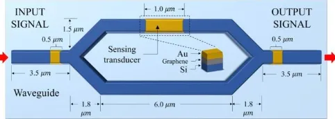
Figure 1: A plasmonic sensor system with practical dimensions given, where the sensing transducer is embedded in the interferometer arm. Both input and output ports are embedded in the silicon-graphene-gold layers for potential mobility sensing-related applications (an electrode). The stacked layer length is 1.0 µm. (Preliminary data on the silicon-graphene-gold layer characteristics were reported previously [28, 30, 32]).
When a source of excitation to be measured, such as an electric field, electrical current, magnetic field is considered, monochromatic light is input into the sensing transducer via the gold layer on the silicon and if there is any change related to the change in phase of light in the sensing
transducer, it will be seen at the interferometer output. Generally, physical environmental changes such as heat, pressure, current, vapor, fluid, gas presence etc. will casue changes in the transducer and as a result this induces the change in OPD of the light in the silicon and in the electron mobility (µ) in the layers. The phenomenon arises when the plasmon waves from the silicon penetrate the graphene via the evanescent wave, from which the excited electrons are conducted in the gold layer, driven at the group velocity (Vd)
of the plasmon waves. This effect allows the device to act as a sensing transducer, where the graphene layer is the active medium. The relationship between the light intensity (I), the group velocity and the electron mobility can be expressed by
I=𝑬𝟐 = ( 𝑽𝒅
𝝁)
𝟐, where V
d = µE, When an electric field E is
applied to the sensing transducer, an electric current is established in the conductor. The density Js of this current is
given by Js = σE. The constant of proportionality, σ, is the
specific conductance or electrical conductivity of the conductor (for gold this is 1.6x10⁸ W-1m-1) [27]-[30]. From
the phase delay term, 𝝋 = 𝟐𝝅∆𝒏𝒆𝒇𝒇
𝝀 L, it can be seen that if λ
and L are constants, it means that there is only a change in the refractive index that can provide the phase delay. In this case, the change in the refractive index can be induced by the direct change in the light path difference, or by the electron mobility in the gold layer, which is ultimately reflected in the refractive index, given by the relationship shown in Equation (1). The resultant sensitivity of the system depends on the mobility and the applied current, which can be seen through the electron mobility and the electrical current via the interferometer output (silicon) and gold layer, respectively. Moreover, a change in the electron mobility in the gold layer will be caused by the change in the gold layer length, which can be caused by heat or pressure on the sensing transducer and such an effect can be utilized for other sensing applications, as required.
III.
SIMULATION RESULTS
[image:3.612.53.294.489.575.2]within the plasmonic transducer relates to a change in the electron mobility and the applied current or voltage into the gold layer, which affects the electron mean free path in the gold layer
.
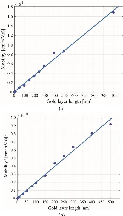
The electron mobility in gold is 42.6 cm2 V-1 s-1 [33, 34], with the simulation result yielding the relationship between the electron mean free path and the electron mobility allowing sensing applications involving mobility changes.The characteristics of the sensing transducer determined with the variations in the electron mobility, the input power and the gold length values were plotted, as shown in Figures 3-5. As a result, the device sensitivity can be presented through the relationship between the mobility output and the change in gold layer lengths, (which is simulated and plotted) and from which the relative mobility sensitivity is given by
~2.0 x 10⁻¹¹𝑚 𝑉−1𝑠−1. The data shown in Figures 3 and 4 can be related to the optical path difference through the relationship 𝒏𝒆𝒇𝒇 = 𝒄
𝒗, where c is the speed of light in vacuum,
and thus the OPD = 𝒄
𝒏𝒆𝒇𝒇 ∆𝒕, where ∆t is the change in time
associated with the measured mobility.
Figure 2: The 3D image obtained using the Optiwave program, where all parameters are given in Figure 1. The input source wavelength is 1.55 µm.
Figure 3: Graph of the electron mobility of the sensing transducer (gold layer) with the input power – here the input power is varied from 0.5-5.0 mW, with the gold layer length fixed at 200 nm
Regarding the phase term in an Equation (1), the change in the output fringe oscillation occurs with time, ∆𝑡, where the peak-to-peak measurement of the output signal is obtained from the slope calculation (at ∆t = 2.5 fs), with the
calculation of the OPD in silicon as 𝑐
𝑛∆𝑡, with, as usual, c
being the speed of light in vacuum, n the material refractive index and the refractive index of a silicon is 1.46. The obtained OPD is ~5.14 x 10⁻⁷m (or 514 nm,) which can also be used to determine the electron mean free path from the
relationship µ= 𝒆𝝉 𝒎=
𝒆𝒅
𝒎𝒗𝑭 [33], where e is the charge, τ is
the mean free time, m is the mass, d is the mean free paths, and vF is the Fermi velocity of the charge carrier.
(a)
(b)
Figure 4: (a) Graph of the electron mobility as a function of the gold layer length at the sensing transducer, where the gold layer length is varied up to 1000 nm. The input power is fixed at 3 mW. (b) Graph of the change in mobility visibility and the gold layer length at the MZI output (seen in Figure 1), where the input power is fixed at 3 mW, the gold length is varied up to 500 nm, and the calculated mobility slope visibility = ~ 2.0 𝑥 10−14𝑚 𝑉−1𝑠−1.
IV. CONCLUSIONS
[image:4.612.336.542.168.530.2] [image:4.612.71.272.301.440.2] [image:4.612.72.274.484.632.2]Page 4 of 4
in light propagation intensity in the MZI arm that can be detected at the MZI output. Thus, the relationship between the change in the electron mobility in the gold layer and the MZI output intensity yields the sensitivity of operation of the device. The relationship between the change in the electron mobility and the electron mean free path in terms of the OPD can be plotted and calculated. From the results obtained, a device sensitivity of~2x10⁻¹⁴ 𝑚 𝑉−1𝑠−1 is obtained. Such device parameters are realistic given the materials and fabrication parameters [35-39], while the approach using the stacked layers of silicon-graphene material were tested and experimentally verified in the literature [40]. Gold forms the basis of the mobility sensor, and other materials can also be applied, with the optimum fabrication parameters to be found the references [34]. The electron mobility related parameters of various material (including the gold), including the electron mean free path, the group velocity, and the average Fermi velocity are given in the literature [27, 38], (where the electron mobility in gold is published as 42.6 cm2 V-1 s-1[38]).
ACKNOWLEDGMENTS
This research is funded by the Foundation for Science and Technology Development of Ton Duc Thang University (FOSTECT), website: http://fostect.tdt.edu.vn, under Grant FOSTECT.2017.BR.07. M.S. Aziz would like to acknowledge for the support and facilities under the UTM Shine Program. V. Koledov would like to acknowledge for the support and facilities under RSF Grant 17-19-01748. K. T. V. Grattan acknowledges the support of the George Daniels Educational Trust and the Royal Academy of Engineering.
REFERENCES
[1] P. Hariharan, “Basics of Interferometry”, Elsevier Inc., Netherland, ISBN: 0-12-373589-0, 2017.
[2] S. Steinlenchner et al., “Quantum-dense metrology”, Nature Photonics, vol. 7, p. 626, 2013.
[3] M. Szuatakowski and N. Palka , “Contrast sensitive fiber optic Michelson interferometer as elongation sensor”, Opto-electron. Rev., vol. 13, no. 1, pp. 19-26, 2005.
[4] D. Shoemaker et al., “Prototype Michelson interferometer with Fabry-Perot cavities”, Appl. Opt., vol. 30, no. 22, pp.3133-3138, 1991. [5] D. Coyne, “Precision Engineering in the Laser Interferometer
Gravitational-wave Observatory (LIGO)”, paper presented in the Proceedings of the 2nd German-American Frontiers of Engineering Symposium, sponsored by the National Academy of Engineering, Univ. of California, Irvine, 1999.
[6] K. Weir et al., “A novel adaptation of the Michelson interferometer for the measurement of vibration”, Lightwave Technol., vol. 10, no. 5, pp. 700-703, 1992.
[7] Y. Jung et al., “Ultra-compact in-line broadband Mach–Zehnder interferometer using a composite leaky hollow-optical-fiber waveguide”, Optics Letters, vol. 33, no. 24, pp. 2934-2936, 2008. [8] D.S. Wei et al., “Mach-Zehnder interferometry using spin- and
valley-polarized quantum Hall edge states in graphene”, Science
Advances , vol. 3, no. 8, p. e1700600, 2017.
[9] J. Ali et al., “A novel plasmonic interferometry and the potential applications”, Results in Physics, 8, 438-441, 2018.
[10] N. Pornsuwancharoen et al., “Multifunction interferometry using the electron mobility visibility and mean free path relationship”, Microscopic Research Technique, Submitted manuscript.
[11] O. Graydon, “Plasmonic interferometry”, Nat. Photon., vol. 6, no. 3, p. 139, 2012.
[12] J.V. Feng et al. , “Nanoscaleplasmonic interferometers for multispectral, high-throughput biochemical sensing”, Nano Lett., vol. 12, no. 2, pp. 602–609, 2011.
[13] D. Morrill et al., “Measuring subwavelength spatial coherence with plasmonic interferometry”, Nature Photonics, vol. 10, pp. 661-687, 2010.
[14] D. Li et al., “Nanoscale optical interferometry with incoherent light”, Scien. Rep., 2016, Article number 20836, 2016.
[15] F. Bartoli et al., “Plasmonic interferometer biosensors”, U.S Patent Number:20140218738A1, Washington, DC : U.S. Patent and Trademark Office, 2014.
[16] Q. Gan and F. Bartoli, “Vertical plasmonicmach-zehnder interferometer”, U.S. Patent number: 20110080589A1, Washington, DC: U.S. Patent and Trademark Office, 2011.
[17] G.C. Dyer et al., “Two-path plasmonic interferometer with integrated detector”, U.S. Patent number: US9297638 B1, Washington, DC: U.S. Patent and Trademark Office, 2016.
[18] Z. Fang et al., “Planar plasmonic focusing and optical transport using CdS nanoribbon”, Vol. 4, no. 1, 75-82, 2010. [19] Z. Fang et al., “Plasmonic coupling of bow tie antennas with Ag
nanorire”, Nano Lett., vol. 11, no. 4,
[20] Z. Fang et al., “Graphene-antenna sandwich photodetector”, Nano Lett., vol. 12, p. 3808, 2012.
[21] Z. Fang et al., Plasmon-induced doping of graphene, ACS Nano, vol. 6, p. 10222, 2012.
[22] D.F. Swearer et al., “Transition-metal decorated aluminum nanocrystals, ACS Nano, DOI: 10.1021/acsnano.7b04960, 2017. [23] P. Pavaskar et al., “A microscopic study of strongly plasmonic Au and
Ag island thin films”, Journal of Applied Physics, vol. 113, p. 034302, 2013.
[24] N. Pornsuwancharoen et al., “Electron driven mobility model by light on the stacked metal-dielectric-interfaces”, Microw. &Opti.Techn.Lett., vol. 59, no. 7, pp. 1704-1709, 2017.
[25] N. Pornsuwancharoen et al., “Micro-current source generated by a WGM of light within a stacked silicon-graphene-Au waveguide”, IEEE Photon. Technol. Lett. Vol. 19, no. 21, pp. 1768-1771, 2017. [26] K.I. Bolotin, “Ultra high electron mobility in suspended graphene”,
Solid State Commun., vol. 146, p. 351, 2008.
[27] E. Ozbay, “Plasmonics: merging photonics and electronics at the nanoscale dimensions”, Science, vol. 311, no. 5758, pp. 189-193, 2006.
[28] I.G. Smolyaninov et al., “Surface plasmon dielectric waveguide”, Appl. Phys. Lett., vol. 87, p. 241106, 2005.
[29] G. Gumbs et al., “Plasmon excitations of multilayer graphene on a conducting substrate”, Sci. Rep, vol. 6, Article number 21063, 2016. [30] P.A. Thomas et al., “Strong coupling of diffraction coupled plasmons and optical waveguide modes in gold stripe dielectric Nano-structures at telecom wavelengths”, Sci. Rep., vol. 7, article number 45196, 2017.
[31] J.D. Bourke and C.T. Chantler, Measurements of electron inelastic mean free paths in materials, Phys. Rev. Lett., vol. 104, p. 206601, 2010. [32] T. Ren-Bing , “Electronics driven plasmon dispersion in AlGaN/GaN
high electron mobility transistors”, Chin. Phys. B, vol. 22, no. 11, p. 117306, 2013.
[33] D. Gall D, “Electron mean free path in elemental metals”, J Appl. Phys., vol. 119, p. 085101, 2016.
[34] G. Baccarani and P. Ostoja, “Electron mobility empirically related to the phosphorus concentration in silicon, Solid State Electron., vol. 18, no. 6, pp. 579-580, 1975.
[35] H.-M. Xin, “Design and fabrication of InP micro-ring resonant detectors”, Opto-electron. Lett., vol. 5, pp. 6-10.
[36] W. Bogaerts et al.,“Silicon micro-ring resonators”, Laser Photon. Rev., vol. 6, no. 1, pp. 47-73, 2012, 2009.
[37] A.S. Prabhu et al., “Extreme miniaturization of silicon add–drop micro-ring filters for VLSI photonics applications”, IEEE Photon. J., vol. 2, no. 3, pp. 436-444, 2010.
[38] K. Liu et al., K, “Fundamental scaling laws in Nano-photonics, Sci. Rep., vol. 6, Article number 37419, 2016.
[39] J.D. Bourke and C.T. Chantler, “Measurements of electron inelastic mean free paths in materials”, Phys. Rev. Lett., vol. 104, p. 206601, 2010.