Raised source/drains for 50 nm MOSFETs using a
silane/dichlorosilane mixture for selective epitaxy
A.M. Waite
a, N.S. Lloyd
a, K. Osman
a, W. Zhang
a, T. Ernst
b, H. Achard
b, Y. Wang
c,
S. Deleonibus
b, P.L.F. Hemment
c, D.M. Bagnall
a, A.G.R. Evans
a, P. Ashburn
a,*a
Department of Electronics and Computer Science, University of Southampton, Highfield, Southampton SO17 1BJ, UK
b
CEA/DRT-LETI Grenoble, 17 Rue des Martyrs, F38054 Grenoble Cedex 9, France
c
Department of Electronic Engineering, University of Surrey, Guildford GU2 7XH, UK
Received 7 January 2004; received in revised form 11 January 2005; accepted 11 January 2005
The review of this paper was arranged by Prof. S. Cristoloveanu
Abstract
A selective epitaxy process for raised sources and drains is investigated, with growth performed at a pressure in the 1 Torr regime, rather than the more common CVD (10Õs of Torr) or UHV–CVD (1–40 mTorr) regimes. It is shown that selective growth can be achieved using a mixture of silane and dichlorosilane without any requirement for Cl2or HCl in the gas stream. The selectivity of the
process can be controlled by varying the silane:dichlorosilane ratio in the gas mixture, with a ratio between 1:1 and 3:1 giving selec-tive growth. Facet-free selecselec-tive epitaxy is achieved, the process is selecselec-tive to silicon nitride and a growth activation energy of 2.4 eV is obtained. Raised source/drain MOSFET devices with channel lengths down to 50 nm have been fabricated and the thickness of the selective epitaxial silicon layer has been varied to investigate the effect of this parameter on device performance. Excellent sub-threshold characteristics are obtained and the sub-sub-threshold slope, S, improves from 102 to 81.9 mV/dec as the raised source/drain thickness is increased from 50 nm to 100 nm. The raised source/drain also improves threshold voltage roll-off and drain induced barrier lowering. A decrease in bothIonandIoffis seen with increasing RSD thickness, but the overallIoff/Iontrade-off is unchanged.
Ó2005 Elsevier Ltd. All rights reserved.
Keywords: Raised source/drain; Selective epitaxy; Silicon epitaxy; MOSFETs
1. Introduction
As MOSFET devices are scaled to decananometer dimensions, good control of short channel effects re-quires the formation of increasingly shallow junctions
[1]. This scaling of the source/drain junction depth leads to undesirable increases in the parasitic series resistance of the source and drain. While increases in source/drain series resistance can be moderated by decreasing the thickness of the sidewall spacer, this has the
disadvan-tage of degrading short channel performance because the highly doped source/drain diffuses beneath the spacer and over-dopes the extension. Raised sources and drains offer an increasingly attractive solution to these problems because the elevation of the source and drain suppresses the sub-diffusion of the source/drain dopant beneath the sidewall spacer [2–4], allowing the spacer to be thinner while maintaining short channel performance.
Selective silicon epitaxy is key to the realisation of raised sources and drains, and this can be achieved in a number of different ways. Several groups[2,5–7]have exploited the Ôincubation periodÕ to achieve selective
0038-1101/$ - see front matter Ó2005 Elsevier Ltd. All rights reserved. doi:10.1016/j.sse.2005.01.019
* Corresponding author. Tel.: +44 2380592886; fax: +44 2380593029.
E-mail address:[email protected](P. Ashburn).
epitaxial growth using SiH4 as the source gas. While
such processes are chlorine-free, they require a high tem-perature to achieve selective growth. For raised sources and drains, a low growth temperature is needed to avoid diffusion of the LDD and pocket implants during epi-taxy. Furthermore, the achievement of selective epitaxy with a sidewall nitride spacer is difficult to achieve with SiH4. Selective growth to silicon nitride has been
re-ported by several groups [8–10] using a variety of gas chemistries such as Si2H6/H2/Cl2, Si2H6/Cl2 and
SiH2Cl2/HCl/H2. However, these processes utilise the
addition of Cl2or HCl to adjust the selectivity. In this
approach, Cl2 or HCl is used in the growth process
and the selectivity is controlled by varying the amount of Cl2/HCl in the gas stream. The minimisation of the
Cl2/HCl content is desirable because degradation of
the surface quality is obtained for high Cl2/HCl contents
and because processes with Cl2or HCl are susceptible to
loading effects[11,12].
The majority of growth processes reported in the lit-erature operate in one of two pressure regimes. UHV– CVD and UHV–RTCVD growth processes use very low growth pressures in the 1–40 mTorr range [10] to take advantage of the ultra-clean environment in a UHV system. Alternatively, CVD growth systems used in many production epitaxy processes tend to operate in the tens of Torr pressure regime [11]. In this paper, a selective growth process for raised sources and drains is investigated in which the growth is performed in the 1 Torr pressure regime. It is shown that selective growth can be achieved using a mixture of silane and dichloro-silane, without using Cl2 or HCl directly and that the
selectivity of the growth can be tuned by varying the proportion of silane and dichlorosilane in the gas mix-ture. The process is shown to be facet-free and selective to silicon nitride gate spacers. This selective epitaxy pro-cess is used to implement raised sources and drains in 50 nm MOSFETs, which are shown to have excellent electrical characteristics. The thickness of the raised source/drain is varied and the effect on transistor short channel performance is characterised.
2. Selective epitaxy using a silane/dichlorosilane mixture
To investigate the effect of the SiH4:SiH2Cl2flow rate
ratio on the growth rate, this ratio was varied from 0:1 to 5:1 with H2carrier gas constant at 100 sccm. A
pro-cess temperature of 850°C and pressure of 1 Torr were chosen as starting conditions. The growth experiments were performed on a series of silicon nitride bars and sili-con windows of variable width from 2.5lm to 20lm to test the selectivity of the process to silicon nitride.Fig. 1
shows the growth rate as a function of silane/dichlorosi-lane flow rate ratio for these growth conditions. When only SiH2Cl2 was used in the process, the growth rate
was negative; i.e. the excess chlorine ions in the gas phase created an etching environment. The substrate sili-con was therefore selectively etched with respect to the nitride masking material. For greater SiH4:SiH2Cl2flow
ratios of 3:1 and 5:1, the process becomes increasingly less selective and polysilicon begins to be deposited on the silicon nitride mask. However, for SiH4:SiH2Cl2flow
ratios between 1:1 and 3:1, the growth is selective to silicon nitride. Experiments have also shown that the growth process is selective to silicon dioxide for these flow ratios.
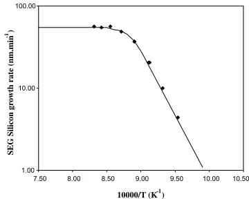
In order to assess the effect of process temperature on selectivity, the process temperature was varied between 930°C and 760°C. A mixture of SiH4/SiH2Cl2/H2gases
was used with at flows of 10/10/100 sccm respectively. The chamber pressure remained constant throughout at 1 Torr. Selectivity was maintained throughout the en-tire temperature range studied. The results of these experiments are shown in the Arrhenius plot in Fig. 2. Above 900°C, the curve shows a constant growth rate of 55 nm/min, indicating that mass transport in the gas phase is the limiting growth mechanism. Below 900°C,
-15 -5 5 15 25 35 45 55 65 75
0 1 2 3 4 5 6
SiH4/DCS flow rate ratio
Gr
o
wth rate (nm.min
-1 )
Decreasing selectivity
DCS only
[image:2.595.318.551.72.206.2]Etch SEG
Fig. 1. Growth rate as a function of silane/dichlorosilane flow rate ratio for a growth temperature of 850°C and a growth pressure of 1 Torr. The hydrogen carrier gas flow was constant at 100 sccm.
1.00 10.00 100.00
7.50 8.00 8.50 9.00 9.50 10.00 10.50 10000/T (K-1)
SEG Silicon gr
o
wth rate (nm.min
-1)
Fig. 2. Growth rate as a function of reciprocal temperature for selective silicon layers grown at temperatures in the range 760–930°C. The growth pressure was 1 Torr and the flow rates were SiH4/SiH2Cl2/
[image:2.595.342.522.545.689.2]the growth rate decreases with decreasing temperature. This classical behaviour indicates that in this tempera-ture range, the process is likely to be limited by a surface reaction. From this region of the curve, an activation energy of 2.4 eV (55 kcal/mol) can be calculated. This value is close to that given by Regolini et al. [8] of 2.6 eV (59 kcal/mol) who used a SiH2Cl2/H2 growth
process. These results suggest that the dissociation of dichlorosilane into SiHCl + HCl is likely to be the rate limiting process, since the dissociation energy of this process is 60 kcal/mol[8]. However, this growth mecha-nism has been achieved without the use of Cl2or HCl in
the gas stream.
Measurements of selective epitaxial layer thickness were made in windows ranging in size from 2.5lm to 20lm, and the thickness was found to be constant to better than ±1%. This indicates that there are no dis-cernable loading effects with this selective epitaxy process for the window sizes measured. The silicon growth rate for all window sizes was found to be 39.4 ± 0.4 nm/min.
Fig. 3shows a cross-section SEM image of an 80 nm
MOS transistor gate stack after the growth of a raised source/drain using SiH4+ SiH2Cl2 in H2 at 750°C. It
can be seen that the surface of the raised source/drain is flat, with no evidence of facets adjacent to the nitride spacer layer. Polycrystalline silicon has been deposited on top of the polysilicon gate during growth and the thickness of this layer is similar to the40 nm thickness of the raised source/drain.
3. Transistor fabrication
Device processing started with the growth of a 180 nm thick LOCOS field oxide and well implantation.
A 2 nm gate oxide was then grown and 150 nm of silicon deposited on top of this oxide to form the poly-silicon gate electrode. The polypoly-silicon was pre-doped by implantation before etch, and gates were defined by electron beam lithography. The polysilicon was then dry etched and source/drain extensions implanted.
Sidewall spacers, 25 nm thick, were created before fabrication of the raised sources and drains. Selective epitaxial silicon layers were then grown in the source and drain regions of the devices as discussed above and shown in Fig. 3. Prior to epitaxy, the wafers were cleaned using an HF etch followed by an IPA rinse
[13]to give a hydrogen terminated surface. No high tem-perature hydrogen bake was performed prior to epitaxy and the growth was performed at 750°C so that the total thermal budget of the process was minimized. Dif-ferent growth times were used for the selective epitaxial silicon layer of 10, 8, 6 and 4 min to give a variation in the thickness of the raised source/drain (RSD). A 10 min growth gave an epitaxial silicon layer that was approxi-mately 100 nm thick and the shorter growths gave pro-portionally thinner layers. After growth of the raised source/drains, the source/drain was implanted into the epitaxial silicon, and the dopants were activated by rapid thermal anneal. Device processing was completed with a back end of a BPSG inter-level dielectric and Ti/ TiN/Al metallisation.
4. Electrical results
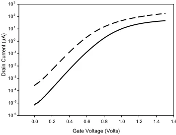
[image:3.595.49.276.69.256.2]Fig. 4shows a typical sub-threshold plot for a 50 nm NMOS transistor with a 100 nm raised source/drain. The characteristics were measured at drain/source biases of 1.5 V and 0.1 V. The transistor has an excellent char-acteristic, with a sub-threshold slope of 81.9 mV/dec. There is no evidence of leakage current at low drain/ source bias, which indicates that there is no bridging of the epitaxy between the gate and the source/drain.
Fig. 3. Cross-sectional SEM view of an 80 nm MOSFET gate stack after raised source/drain growth. The growth was performed at 750°C.
Gate Voltage (Volts)
0.0 0.2 0.4 0.6 0.8 1.0 1.2 1.4 1.6
Drain Current (
µ
A)
10-6 10-5 10-4 10-3 10-2 10-1 100 101 102 103
[image:3.595.336.513.554.690.2]No evidence of bridging was found on any of the devices measured or on any of the SEM cross-sections. DIBL at a drain bias of 1.5 V is 107 mV/V.
A plot of threshold voltage as a function of device channel length is shown inFig. 5for n-channel transis-tors with different thicknesses of raised source/drain and for a reference transistor without a raised source/drain. In all cases, the threshold voltage decreases sharply for channel lengths below about 0.2lm due to short chan-nel effects. The threshold voltage decrease is biggest for the reference transistor and smallest for the transis-tor with a 100 nm RSD. The threshold voltage decrease becomes progressively smaller as the RSD thickness in-creases from 40 to 100 nm. Devices with thinner epitax-ial silicon layers were also measured, but the effect of the raised source/drain on the threshold voltage was small. These results indicate that the raised source/drain is sup-pressing short channel effects.
The threshold voltage roll-off (the difference between the threshold voltage of 50 nm devices and long channel devices) is shown inFig. 6as a function of the epitaxial silicon layer thickness in the raised source/drain for 50 nm n-channel transistors. The effect of the raised source/drain in reducing the threshold voltage roll-off can clearly be seen. The threshold voltage roll-off of the reference devices (with no raised source/drain
struc-ture) is 198 mV, compared to just 53 mV for the devices with the 100 nm thick raised source/drains.
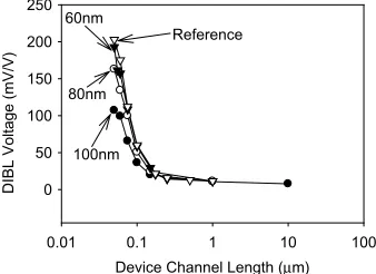
Fig. 7shows a plot of DIBL as a function of channel length for n-channel transistors with different RSD thickness. The DIBL was measured at Vds= 0.1 V and Vds= 1.5 V. It can be seen that raised source/drains give
an improvement in DIBL performance, particularly for a 50 nm channel length. The improvement in DIBL is particularly marked for the 100 nm RSD, which has a DIBL of 107 mV/V, compared with 193 mV/V for the reference transistor.
The sub-threshold slope (S) of 50 nm devices is plot-ted against raised source/drain thickness in Fig. 8. The sub-threshold slopes (S) of these small devices are signif-icantly improved by the addition of a raised source/ drain. For example, the reference device has a sub-threshold slope (S) of 102 mV/dec, compared with 101.5 mV/dec, 94.8 mV/dec and 81.9 mV/dec for devices with 60 nm, 80 nm and 100 nm thick raised source/ drains respectively.
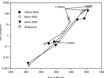
Fig. 9 shows the off-current Ioff as a function of the
on-current Ion for n-channel transistors. Ion was
mea-sured at Vgs=Vds= 1.5 V, and Ioff was measured at
Device Channel Length (µm)
0.01 0.1 1 10 100
Threshold Voltage (Volts)
0.40 0.45 0.50 0.55 0.60 0.65 0.70 0.75
100nm
80nm
60nm
[image:4.595.349.518.366.489.2]Reference
Fig. 5. Transistor threshold voltage as a function of channel length for devices with various thicknesses of raised source/drain.
Epitaxial Silicon Thickness (µm)
0 20 40 60 80 100 120
Threshold Voltage Roll Off (Volts)
[image:4.595.85.262.394.524.2]0.04 0.06 0.08 0.10 0.12 0.14 0.16 0.18 0.20 0.22
Fig. 6. Threshold voltage roll-off as a function of the thickness of the selective silicon raised source/drain.
Device Channel Length (µm)
0.01 0.1 1 10 100
DIBL Voltage (mV/V) 0 50 100 150 200 250
100nm 80nm 60nm
Reference
Fig. 7. DIBL voltage (in mV/V) as a function of device channel length for n-channel transistors with various thicknesses of raised source/ drain. The DIBL was measured between drain voltages of 0.1 V and 1.5 V.
Epitaxial Silicon Thickness (m) 0 20 40 60 80 100 120 Subthreshold Slope (mV/dec) 80
85 90 95 100 105
[image:4.595.351.515.574.698.2] [image:4.595.84.260.578.709.2]Vgs= 0 V, Vds= 1.5 V. The 50 nm devices are marked
on the graph and these devices show that while increas-ing the thickness of the raised source/drain reducesIon,
it also reduces Ioff. However, for a given value of Ioff,
all the data lies on a single line that there is no degrada-tion in theIon/Ioff trade-off, even for the thickest raised
source/drain of 100 nm.
The above results show that the addition of the raised source/drain suppresses both the short channel effect and DIBL. This effect can be attributed to the effect of the raised source/drain (into which the source/drain im-plant is made) in reducing the amount of lateral diffu-sion of the highly doped source and drain under the sidewall spacers. This has the effect of reducing the amount of dopant diffusing into the extensions during processing. Consequently the extensions of the raised source/drain devices are shallower and more resistive than those of the silicon reference device. This effect is more marked as the thickness of the raised source drain is increased. Similar results were reported by Gwoziecki et al.[3], Lee et al.[4]and Yamakawa et al.[14]on tran-sistors with larger geometry raised sources and drains and by Huang et al.[15]on transistors with SiGe raised sources and drains.
The above results show an increase in the steepness of the sub-threshold slope as the thickness of the raised source/drain is increased. This effect can be explained by the better gate control on the channel potential as the shallower junctions reduce the penetration of the electric field from the source and drain into the channel. This effect also accounts for the better short channel behaviour and improved DIBL. A similar improvement in sub-threshold slope S was observed by Ohguro et al.
[16]in devices with channel lengths ranging from 10lm down to 0.1lm. In this work we saw little improvement in the device characteristics for devices with raised source/drains thinner than 60 nm. Ohguro et al.[17]also saw no improvement in DIBL for devices with 50 nm
thick epitaxial layers, but better control of DIBL in devices with 100 nm thick epitaxial layers. The higher resistivity of the extensions and reduction in short chan-nel threshold roll-off accounts for the loss of current drive in the raised devices. This can be compensated for by optimisation of the source/drain implant energy for the raised devices.
The results inFig. 9are very promising, and show that the inclusion of a raised source/drain gives no degradation of the overall trade-off betweenIonandIoff. This result is
significant for devices featuring RSD structures since it means that when an optimised source/drain implant is performed, good Ion/Ioff properties are achievable.
Fur-thermore, due to the additional silicon thickness available for salicidation, the RSD improves the compatibility of scaled devices with existing salicidation processes.
5. Conclusions
A selective epitaxy for raised sources and drains has been studied in which the growth was performed in the 1 Torr pressure regime, rather than the more com-mon 1–40 mTorr regime used in UHV–CVD or the 10Õs of Torr regime used in CVD. It has been shown that selective epitaxy can be achieved using a mixture of si-lane and dichlorosisi-lane, without the use of Cl2or HCl
in the gas stream. The selectivity of the epitaxy is con-trolled by varying the proportion of dichlorosilane in the growth process. Pure dichlorosilane gives etching of the silicon surface, pure silane gives non-selective epi-taxy and silane/dichlorosilane ratios in the range 1:1 to 3:1 give selective epitaxy. The process is facet-free and selective to silicon nitride. 50 nm MOSFETs have been fabricated incorporating raised source/drains grown using this selective epitaxy process. Devices with the raised sources and drains have improved sub-threshold slopes, reduced threshold voltage roll-off and reduced drain induced barrier lowering compared with reference transistors. This improvement in short channel charac-teristics increases as the thickness of the raised source/ drain increases. Both Ion and Ioff decrease as the
thick-ness of the raised source/drain increases, but the overall trade-off between IonandIoffis not degraded.
Acknowledgment
This work was carried out as part of the SIGMOS Framework 5 project. The European Commission is acknowledged for funding this work.
References
[1] Liu ZH, Hu C, Huang JH, Chan TY, Jeng MC, Ko PK, et al. Threshold voltage model for deep sub micrometer MOSFETs. IEEE Trans Electron Dev 1993;40(1):86–95.
Ion (µA/µm)
250 300 350 400 450 500 550
Ioff (nA/
µ
m)
0.001 0.01 0.1 1 10 100 1000
L=50nm L=50nm
100nm RSD
80nm RSD
60nm RSD
[image:5.595.76.251.69.200.2]Reference
Fig. 9. Off state current, measured at Vgs= 0 V, Vds= 1.5 V as a
function of on state current measured at Vgs=Vds= 1.5 V for
n-channel transistors with raised source/drain thicknesses of 60, 80 and 100 nm. Devices with a channel length of 50 nm are highlighted to show how the thickness of the raised source/drain influences theIon/Ioff
[2] Afshar-Hanaii N, Peerlings J, Evans AGR, Carter JC. Improved hot electron degradation in nMOSFETs with elevated source and drain structures realized by SEG of silicon using silane only. Electron Lett 1993;29(17):1586–7.
[3] Gwoziecki R, Jurczak M, Skotnicki T, Regolini J-L, Paoli M. Suitability of elevated source/drain for deep submicron CMOS. In: Proceedings of the ESSDERC. Leuven, Belgium, 1999. p. 384–7.
[4] Lee JH, Lee SC, Kwak NY, Yeo IS, Yeom CY, Ritterbush S, et al. High performance buried channel pFETs using elevated source/drain structure with self-aligned epitaxial silicon sliver (SESS). In: Proceedings of the SSDM. Tokyo, Japan, 1999. p. 38–9.
[5] Ishitani A, Kitajima H, Endo N, Kasai N. Silicon selective epitaxial growth and electrical properties of epi/sidewall inter-faces. Jpn J Appl Phys 1989;28(5):841–8.
[6] Parker GJ, Bonar JM, Starbuck CMK. Long incubation times for selective epitaxial growth of silicon using silane only. Electron Lett 1991;27(17):1595–7.
[7] Murota J, Nakamura N, Kato M, Mikashiba N, Ohmi T. Low temperature silicon selective deposition and epitaxy on silicon using the thermal decomposition of silane under ultraclean environment. Appl Phys Lett 1989;54(11):1007–9.
[8] Regolini JL, Bensahel D, Scheid E, Mercier J. Selective epitaxial silicon growth in the 650–1100°C range in a reduced pressure chemical vapour deposition reactor using dichlorosilane. Appl Phys Lett 1989;54(7):658–9.
[9] Racanelli M, Greve DW, Hatalis MK, van Yzendoorn LJ. Alternative surface cleaning approaches for ultra high vacuum chemical vapour deposition of Si and GeSi. J Electrochem Soc 1991;138(12):3783–9.
[10] Violette KE, OÕNeil PA, Ozturk MC, Christensen K, Maher DM. On the role of chlorine in selective silicon epitaxy by chemical vapour deposition. J Electrochem Soc 1996;143(10):3290–6. [11] Terpstra D, DeBoer WB, Slotboom JW. High performance Si–
SiGe HBTs SiGe technology development in ESPRIT project 8001 TIBIA: an overview. Solid-State Electron 1997;41:1493– 502.
[12] Kiyota Y, Udo T, Hashimoto T, Kodama A, Shimamoto H, Hayami R, et al. HCl free selective epitaxial SiGe growth by LPCVD for high frequency HBTs. IEEE Trans Electron Dev 2002;49(5):739–45.
[13] Waite AM, Lloyd NS, Ashburn P, Evans AGR, Ernst T, Achard H, et al. Raised source/drain for 50 nm MOSFETs: effect of epitaxy layer thickness on short channel effects. In: Proceedings of the ESSDERC. 2003. p. 223–6.
[14] Yamakawa S, Sugihara K, Furukawa T, Nishioka Y, Nakahata T, Abe Y, et al. Drivability improvement on deep-submicron MOSFETs by elevation of source/drain regions. IEEE Electron Dev Lett 1999;20(7):366–8.
[15] Huang HJ, Chen KM, Huang TY, Chao TS, Huang GW, Chien CH, et al. Improved low temperature characteristics of P-Channel MOSFETs with Si1 xGexraised source and drain. IEEE Trans
Electron Dev 2001;48(8):1627–31.
[16] Ohguro T, Sugiyama N, Imai S, Usuda K, Saito M, Yoshitomi T, et al. Undoped epitaxial Si channel n-MOSFET grown by UHV– CVD with preheating. IEEE Trans Electron Dev 1998;45(3): 710–6.