Digital Logic and
Microprocessor Design
With VHDL
,6%1
Contents ... Preface ...
Chapter 1 Designing Microprocessors
...
1.1 Overview of a Microprocessor ... 1.2 Design Abstraction Levels... 1.3 Examples of a 2-to-1 Multiplexer ... 1.3.1 Behavioral Level... 1.3.2 Gate Level... 1.3.3 Transistor Level ... 1.4 Introduction to VHDL ... 1.5 Synthesis... 1.6 Going Forward... 1.7 Summary Checklist... 1.8 Problems ...Chapter 2 Digital Circuits
... 2
2.1 Binary Numbers... 3 2.2 Binary Switch ... 2.3 Basic Logic Operators and Logic Expressions ... 2.4 Truth Tables... 2.5 Boolean Algebra and Boolean Function ... 2.5.1 Boolean Algebra ... 2.5.2 * Duality Principle ... 2.5.3 Boolean Function and the Inverse... 2.6 Minterms and Maxterms... 2.6.1 Minterms... 2.6.2 * Maxterms ... 2.7 Canonical, Standard, and non-Standard Forms... 2.8 Logic Gates and Circuit Diagrams... 2.9 Example: Designing a Car Security System ... 2.10 VHDL for Digital Circuits... 2.10.1 VHDL code for a 2-input NAND gate... 2.10.2 VHDL code for a 3-input NOR gate... 2.10.3 VHDL code for a function ... 2.11 Summary Checklist... 2.12 Problems ...Chapter 3 Combinational Circuits
...
3.1 Analysis of Combinational Circuits...3.7 VHDL for Combinational Circuits ... 3.7.1 Structural BCD to 7-Segment Decoder... 3.7.2 Dataflow BCD to 7-Segment Decoder ... 3.7.3 Behavioral BCD to 7-Segment Decoder... 3.8 Summary Checklist... 3.9 Problems ...
Chapter 4 Standard Combinational Components
...
4.1 Signal Naming Conventions ... 4.2 Adder ... 4.2.1 Full Adder... 4.2.2 Ripple-carry Adder ... 4.2.3 * Carry-lookahead Adder... 4.3 Two’s Complement Binary Numbers ... 4.4 Subtractor... 4.5 Adder-Subtractor Combination... 4.6 Arithmetic Logic Unit... 4.7 Decoder... 4.8 Encoder... 4.8.1 * Priority Encoder... 4.9 Multiplexer ... 4.9.1 * Using Multiplexers to Implement a Function ... 4.10 Tri-state Buffer ... 4.11 Comparator ... 4.12 Shifter ... 4.12.1 * Barrel Shifter ... 4.13 * Multiplier ... 4.14 Summary Checklist... 4.15 Problems ...Chapter 5 * Implementation Technologies
...
5.1 Physical Abstraction ... 5.2 Metal-Oxide-Semiconductor Field-Effect Transistor (MOSFET)... 5.3 CMOS Logic... 5.4 CMOS Circuits ... 5.4.1 CMOS Inverter ... 5.4.2 CMOS NAND gate... 5.4.3 CMOS AND gate...5.4.4 CMOS NOR and OR Gates ...1
5.4.5 Transmission Gate ... 5.4.6 2-input Multiplexer CMOS Circuit...1
5.4.7 CMOS XOR and XNOR Gates...1
5.5 Analysis of CMOS Circuits ... 1
5.6 Using ROMs to Implement a Function ... 15
5.7 Using PLAs to Implement a Function ...1
6.2 SR Latch ... 6.3 SR Latch with Enable ... 6.4 D Latch ... 6.5 D Latch with Enable ... 6.6 Clock...
6.7 D Flip-Flop ... 1
6.7.1 * Alternative Smaller Circuit ...1
6.8 D Flip-Flop with Enable ...1
6.9 Asynchronous Inputs ...1
6.10 Description of a Flip-Flop ... 6.10.1 Characteristic Table ...1
6.10.2 Characteristic Equation...1
6.10.3 State Diagram ...1
6.10.4 Excitation Table...1
6.11 Timing Issues...1
6.12 Example: Car Security System – Version 2... 6.13 VHDL for Latches and Flip-Flops...1
6.13.1 Implied Memory Element ...1
6.13.2 VHDL Code for a D Latch with Enable ... 6.13.3 VHDL Code for a D Flip-Flop ... 19
6.13.4 VHDL Code for a D Flip-Flop with Enable and Asynchronous Set and Clear ... 6.14 * Flip-Flop Types ... 6.14.1 SR Flip-Flop ... 6.14.2 JK Flip-Flop... 6.14.3 T Flip-Flop... 6.15 Summary Checklist... 6.16 Problems ...
Chapter 7 Sequential Circuits
... 2
7.1 Finite-State-Machine (FSM) Models... 7.2 State Diagrams... 7.3 Analysis of Sequential Circuits... 7.3.1 Excitation Equation ... 7.3.2 Next-state Equation ... 7.3.3 Next-state Table... 7.3.4 Output Equation... 7.3.5 Output Table ... 7.3.6 State Diagram ...0
7.8.2 State Encoding ... 7.8.3 Choice of Flip-Flops ... 7.9 Summary Checklist... 7.10 Problems ...
Chapter 8 Standard Sequential Components
... 2
8.1 Registers ... 8.2 Shift Registers... 8.2.1 Serial-to-Parallel Shift Register ... 8.2.2 Serial-to-Parallel and Parallel-to-Serial Shift Register ... 8.3 Counters... 8.3.1 Binary Up Counter... 8.3.2 Binary Up-Down Counter... 8.3.3 Binary Up-Down Counter with Parallel Load ... 8.3.4 BCD Up Counter ... 8.3.5 BCD Up-Down Counter ... 8.4 Register Files ... 8.5 Static Random Access Memory...2
8.6 * Larger Memories ... 8.6.1 More Memory Locations ...2
8.6.2 Wider Bit Width ...2
8.7 Summary Checklist...2
8.8 Problems ...2
Chapter 9 Datapaths
... 2
9.1 Designing Dedicated Datapaths... 9.1.1 Selecting Registers... 9.1.2 Selecting Functional Units... 9.1.3 Data Transfer Methods ... 9.1.4 Generating Status Signals ... 9.2 Using Dedicated Datapaths... 9.3 Examples of Dedicated Datapaths ... 9.3.1 Simple IF-THEN-ELSE... 9.3.2 Counting 1 to 10 ... 9.3.3 Summation of n down to 1... 9.3.4 Factorial ... 9.3.5 Count Zero-One ... 9.4 General Datapaths... 9.5 Using General Datapaths ... 9.6 A More Complex General Datapath ... 9.7 Timing Issues... 9.8 VHDL for Datapaths... 9.8.1 Dedicated Datapath... 9.8.2 General Datapath ... 9.9 Summary Checklist... 9.10 Problems ...
10.3 Generating Status Signals ... 10.4 Timing Issues... 10.5 Standalone Controllers... 10.5.1 Rotating Lights ... 10.5.2 PS/2 Keyboard Controller...
10.5.3 VGA Monitor Controller ...6
10.6 * ASM Charts and State Action Tables ... 37 10.6.1 ASM Charts ...37 10.6.2 State Action Tables...0
10.7 VHDL for Control Units...1
10.8 Summary Checklist...2
10.9 Problems ...4
Chapter 11 Dedicated Microprocessors
...
11.1 Manual Construction of a Dedicated Microprocessor ... 11.2 Examples ... 11.2.1 Greatest Common Divisor ... 11.2.2 Summing Input Numbers... 11.2.3 High-Low Guessing Game ... 11.2.4 Finding Largest Number ... 11.3 VHDL for Dedicated Microprocessors ... 11.3.1 FSM + D Model... 11.3.2 FSMD Model ... 11.3.3 Behavioral Model ... 11.4 Summary Checklist... 11.5 Problems ...Chapter 12 General-Purpose Microprocessors
...
12.1 Overview of the CPU Design ... 12.2 The EC-1 General-Purpose Microprocessor ... 12.2.1 Instruction Set ... 12.2.2 Datapath...512.2.3 Control Unit ... 12.2.4 Complete Circuit... 12.2.5 Sample Program...0
12.2.6 Simulation... 12.2.7 Hardware Implementation ...2
12.3 The EC-2 General-Purpose Microprocessor ...3
12.3.1 Instruction Set ... 12.3.2 Datapath...4
12.3.3 Control Unit ...5
12.3.4 Complete Circuit...8
12.3.5 Sample Program...9
12.3.6 Hardware Implementation ...1
12.4 VHDL for General-Purpose Microprocessors ...2
12.4.1 Structural FSM+D ...2
12.4.2 Behavioral FSMD ...9
12.5 Summary Checklist...2
A.1.1 Preparing a Folder for the Project... A.1.2 Starting MAX+plus II... A.1.3 Starting the Graphic Editor ... A.2 Using the Graphic Editor ... 4 A.2.1 Drawing Tools ... 4 A.2.2 Inserting Logic Symbols ... 4 A.2.3 Selecting, Moving, Copying, and Deleting Logic Symbols... A.2.4 Making and Naming Connections ...6 A.2.5 Selecting, Moving and Deleting Connection Lines ... A.3 Specifying the Top-Level File and Project ... A.3.1 Saving the Schematic Drawing... A.3.2 Specifying the Project... A.4 Synthesis for Functional Simulation... A.5 Circuit Simulation... A.5.1 Selecting Input Test Signals ... A.5.2 Customizing the Waveform Editor ... A.5.3 Assigning Values to the Input Signals ... A.5.4 Saving the Waveform File ... A.5.5 Starting the Simulator ... A.6 Creating and Using the Logic Symbol...
Appendix B VHDL Entry Tutorial 2
...
B.1 Getting Started ...B.1.1 Preparing a Folder for the Project... B.1.2 Starting MAX+plus II... B.1.3 Creating a Project ... B.1.4 Editing the VHDL Source Code ... B.2 Synthesis for Functional Simulation... B.3 Circuit Simulation... B.3.1 Selecting Input Test Signals ... B.3.2 Customizing the Waveform Editor ... B.3.3 Assigning Values to the Input Signals ... B.3.4 Saving the Waveform File ... B.3.5 Starting the Simulator ...
Appendix C UP2 Programming Tutorial 3
...
C.1 Getting Started ...C.1.1 Preparing a Folder for the Project... C.1.2 Creating a Project ... C.1.3 Viewing the Source File ... C.2 Synthesis for Programming the PLD ... C.3 Circuit Simulation... C.4 Using the Floorplan Editor ... C.4.1 Selecting the Target Device ... C.4.2 Maping the I/O Pins with the Floorplan Editor... C.5 Fitting the Netlist and Pins to the PLD ... C.6 Hardware Setup ... C.6.1 Installing the ByteBlaster Driver ... C.6.2 Jumper Settings... C.6.3 Hardware Connections... C.7 Programming the PLD ...
C.9.3 General Pin Assignments... C.9.4 Two Pushbutton Switches... C.9.5 16 DIP Switches ... C.9.6 16 LEDs ... C.9.7 7-Segment LEDs... C.9.8 Clock... C.10 FLEX10K EPF10K70RC240-4 Summary... C.10.1 JTAG Jumper Settings ... C.10.2 Prototyping Resources for Use ... C.10.3 Two Pushbutton Switches... C.10.4 8 DIP Switches ... C.10.5 7-Segment LEDs... C.10.6 Clock... C.10.7 PS/2 Port ... C.10.8 VGA Port...
Appendix D VHDL Summary
...
D.1 Basic Language Elements...D.1.1 Comments ... D.1.2 Identifiers... D.1.3 Data Objects ... D.1.4 Data Types ... D.1.5 Data Operators ... D.1.6 ENTITY... D.1.7 ARCHITECTURE... D.1.8 GENERIC ... D.1.9 PACKAGE ... D.2 Dataflow Model Concurrent Statements... D.2.1 Concurrent Signal Assignment ...0 D.2.2 Conditional Signal Assignment ... D.2.3 Selected Signal Assignment... D.2.4 Dataflow Model Example ...2 D.3 Behavioral Model Sequential Statements ...
Preface
This book is about the digital logic design of microprocessors. It is intended to provide both an understanding of the basic principles of digital logic design, and how these fundamental principles are applied in the building of complex microprocessor circuits using current technologies. Although the basic principles of digital logic design have not changed, the design process, and the implementation of the circuits have changed. With the advances in fully integrated modern computer aided design (CAD) tools for logic synthesis, simulation, and the implementation of circuits in programmable logic devices (PLDs) such as field programmable gate arrays (FPGAs), it is now possible to design and implement complex digital circuits very easily and quickly.
Many excellent books on digital logic design have followed the traditional approach of introducing the basic principles and theories of logic design, and the building of separate combinational and sequential components. However, students are left to wonder about the purpose of these individual components, and how they are used in the building of microprocessors – the ultimate in digital circuits. One primary goal of this book is to fill in this gap by going beyond the logic principles, and the building of individual components. The use of these principles and the individual components are combined together to create datapaths and control units, and finally the building of real dedicated custom microprocessors and general-purpose microprocessors.
Previous logic design and implementation techniques mainly focus on the logic gate level. At this low level, it is difficult to discuss larger and more complex circuits beyond the standard combinational and sequential circuits. However, with the introduction of the register-transfer technique for designing datapaths, and the concept of a finite-state machine for control units, we can easily implement an arbitrary algorithm as a dedicated microprocessor in hardware. The construction of a general-purpose microprocessor then comes naturally as a generalization of a dedicated microprocessor.
With the provided CAD tool, and the optional FPGA hardware development kit, students can actually implement these microprocessor circuits, and see them execute, both in software simulation, and in hardware. The book contains many interesting examples with complete circuit schematic diagrams, and VHDL codes for both simulation and implementation in hardware. With the hands-on exercises, the student will learn not only the principles of digital logic design, but also in practice, how circuits are implemented using current technologies.
To actually see your own microprocessor comes to life in real hardware is an exciting experience. Hopefully, this will help the students to not only remember what they have learned, but will also get them interested in the world of digital circuit design.
Advanced and Historical Topics
Sections that are designated with an asterisk ( * ) are either advanced topics, or topics for a historical perspective. These sections may be skipped without any loss of continuity in learning how to design a microprocessor.
Summary Checklist
There is a chapter summary checklist at the end of each chapter. These checklists provide a quick way for students to evaluate whether they have understood the materials presented in the chapter. The items in the checklists are divided into two categories. The first set of items deal with new concepts, ideas, and definitions, while the second set deals with practical how to do something types.
Design of Circuits Using VHDL
On the other hand, by studying the VHDL codes, the student can not only learn the use of a hardware description language, but also learn how digital circuits can be designed automatically using a synthesizer. This book provides a basic introduction to VHDL, and uses the learn-by-examples approach. In writing VHDL code at the dataflow and behavioral levels, the student will see the power and usefulness of a state-of-the-art CAD synthesis tool.
Using this Book
This book can be used in either an introductory, or a more advanced course in digital logic design. For an introductory course with no previous background in logic, Chapters 1 to 4 are intended to provide the fundamental concepts in designing combinational circuits, and Chapters 6 to 8 cover the basic sequential circuits. Chapters 9 to 12 on microprocessor design can be introduced and covered lightly. For an advanced course where students already have an exposure to logic gates and simple digital circuits, Chapters 1 to 4 will serve as a review. The focus should be on the register-transfer design of datapaths and control units, and the building of dedicated and general-purpose microprocessors as covered in Chapters 9 to 12. A lab component should complement the course where students can have a hands-on experience in implementing the circuits presented using the included CAD software, and the optional development kit. A brief summary of the topics covered in each chapter follows.
Chapter 1 – Designing a Microprocessor gives an overview of the various components of a microprocessor circuit, and the different abstraction levels in which a circuit can be designed.
Chapter 2 – Digital Circuits provides the basic principles and theories for designing digital logic circuits by introducing the use of truth tables and Boolean algebra, and how the theories get translated into logic gates, and circuit diagrams. A brief introduction to VHDL is also given.
Chapter 3 – Combinational Circuits shows how combinational circuits are analyzed, synthesized and reduced.
Chapter 4 – Combinational Components discusses the standard combinational components that are used as building blocks for larger digital circuits. These components include adder, subtractor, arithmetic logic unit, decoder, encoder, multiplexer, tri-state buffer, comparator, shifter, and multiplier. In a hierarchical design, these components will be used to build larger circuits such as the microprocessor.
Chapter 5 – Implementation Technologies digresses a little by looking at how logic gates are implemented at the transistor level, and the various programmable logic devices available for implementing digital circuits.
Chapter 6 – Latches and Flip-Flops introduces the basic storage elements, specifically, the latch and the flip-flop.
Chapter 7 – Sequential Circuits shows how sequential circuits in the form of finite-state machines, are analyzed, and synthesized. This chapter also shows how the operation of sequential circuits can be precisely described using state diagrams.
Chapter 8 – Sequential Components discusses the standard sequential components that are used as building blocks for larger digital circuits. These components include register, shift register, counter, register file, and memory. Similar to the combinational components, these sequential components will be used in a hierarchical fashion to build larger circuits.
Chapter 9 – Datapaths introduces the register-transfer design methodology, and shows how an arbitrary algorithm can be performed by a datapath.
Chapter 10 – Control Units shows how a finite-state machine (introduced in Chapter 7) is used to control the operations of a datapath so that the algorithm can be executed automatically.
Chapter 11 – Dedicated Microprocessors ties the separate datapath and control unit together to form one coherent circuit – the custom dedicated microprocessor. Several complete dedicated microprocessor examples are provided.
Software and Hardware Packages
The newest student edition of Altera’s MAX+Plus II CAD software is included with this book on the accompanying CD-ROM. The optional UP2 hardware development kit is available from Altera at a special student price. An order form for the kit can be obtained from Altera’s website at www.altera.com.
Source files for all the circuit drawings and VHDL codes presented in this book can also be found on the accompanying CD-ROM.
Website for the Book
The website for this book is located at the following URL:
www.cs.lasierra.edu/~ehwang
The website provides many resources for both faculty and students.
Designing Microprocessors
Control Signals
Status Signals
MUX '0'
Data Inputs
Data Outputs
Datapath
ALU
Register ff
8
8 8
Output Logic
Next-state Logic
Control Inputs
Control Outputs
State Memory
Register
Control Unit
ff
Being a computer science or electrical engineering student, you probably have assembled a PC before. You may have gone out to purchase the motherboard, CPU (central processing unit), memory, disk drive, video card, sound card, and other necessary parts, assembled them together, and have made yourself a state-of-the-art working computer. But have you ever wondered how the circuits inside those IC (integrated circuit) chips are designed? You know how the PC works at the system level by installing the operating system and seeing your machine come to life. But have you thought about how your PC works at the circuit level, how the memory is designed, or how the CPU circuit is designed?
In this book, I will show you from the ground up, how to design the digital circuits for microprocessors, also known as CPUs. When we hear the word “microprocessor,” the first thing that probably comes to many of our minds is the Intel Pentium® CPU, which is found in most PCs. However, there are many more microprocessors that are not Pentiums, and many more microprocessors that are used in areas other than the PCs.
Microprocessors are the heart of all “smart” devices, whether they be electronic devices or otherwise. Their smartness comes as a direct result of the decisions and controls that microprocessors make. For example, we usually do not consider a car to be an electronic device. However, it certainly has many complex, smart electronic systems, such as the anti-lock brakes and the fuel-injection system. Each of these systems is controlled by a microprocessor. Yes, even the black, hardened blob that looks like a dried-up and pressed-down piece of gum inside a musical greeting card is a microprocessor.
There are generally two types of microprocessors: general-purpose microprocessors and dedicated microprocessors. General-purpose microprocessors, such as the Pentium CPU, can perform different tasks under the control of software instructions. General-purpose microprocessors are used in all personal computers.
Dedicated microprocessors, also known as application-specific integrated circuits (ASICs), on the other hand, are designed to perform just one specific task. For example, inside your cell phone, there is a dedicated microprocessor that controls its entire operation. The embedded microprocessor inside the cell phone does nothing else but control the operation of the phone. Dedicated microprocessors are, therefore, usually much smaller and not as complex as general-purpose microprocessors. However, they are used in every smart electronic device, such as the musical greeting cards, electronic toys, TVs, cell phones, microwave ovens, and anti-lock break systems in your car. From this short list, I’m sure that you can think of many more devices that have a dedicated microprocessor inside them. Although the small dedicated microprocessors are not as powerful as the general-purpose microprocessors, they are being sold and used in a lot more places than the powerful general-purpose microprocessors that are used in personal computers.
Designing and building microprocessors may sound very complicated, but don’t let that scare you, because it is not really all that difficult to understand the basic principles of how microprocessors are designed. We are not trying to design a Pentium microprocessor here, but after you have learned the material presented in this book, you will have the basic knowledge to understand how it is designed.
This book will show you in an easily understandable approach, starting with the basics and leading you through to the building of larger components, such as the arithmetic logic unit (ALU), register, datapath, control unit, and finally to the building of the microprocessor — first dedicated microprocessors, and then general-purpose microprocessors. Along the way, there will be many sample circuits that you can try out and actually implement in hardware using the optional Altera UP2 development board. These circuits, forming the various components found inside a microprocessor, will be combined together at the end to produce real, working microprocessors. Yes, the exciting part is that at the end, you actually can implement your microprocessor in a real IC, and see that it really can execute software programs or make lights flash!
1.1 Overview of a Microprocessor
the focus is on the design of the digital circuitry of the microprocessor, the memory, and other supporting digital logic circuits.
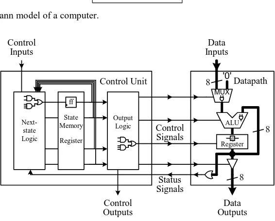
The logic circuit for the microprocessor can be divided into two parts: the datapath and the control unit, as shown in Figure 1.1. Figure 1.2 shows the details inside the control unit and the datapath. The datapath is responsible for the actual execution of all data operations performed by the microprocessor, such as the addition of two numbers inside the arithmetic logic unit (ALU). The datapath also includes registers for the temporary storage of your data. The functional units inside the datapath, which in our example includes the ALU and the register, are connected together with multiplexers and data signal lines. The data signal lines are for transferring data between two functional units. Data signal lines in the circuit diagram are represented by lines connecting two functional units. Sometimes, several data signal lines are grouped together to form a bus. The width of the bus (that is, the number of data signal lines in the group) is annotated next to the bus line. In the example, the bus lines are thicker and are 8-bits wide. Multiplexers, also known as MUXes, are for selecting data from two or more sources to go to one destination. In the sample circuit, a 2-to-1 multiplexer is used to select between the input data and the constant ‘0’ to go to the left operand of the ALU. The output of the ALU is connected to the input of the register. The output of the register is connected to three different destinations: (1) the right operand of the ALU, (2) an OR gate used as a comparator for the test “not equal to 0,” and (3) a tri-state buffer. The tri-state buffer is used to control the output of the data from the register.
Input
Microprocessor Memory
Output Control
[image:17.612.165.448.376.604.2]Unit Datapath
Figure 1.1. Von Neumann model of a computer.
Control Signals
Status Signals
MUX '0'
Data Inputs
Data Outputs
Datapath
ALU Register
ff
8
8 8
Output Logic
Next-state Logic
Control Inputs
Control Outputs
State Memory Register
Control Unit
ff
Figure 1.2. Internal parts of a microprocessor.
determining what the next state should be for the machine. And the output logic is the circuit for generating the actual control signals for controlling the datapath.
Every digital logic circuit, regardless of whether it is part of the control unit or the datapath, is categorized as either a combinational circuit or a sequential circuit. A combinational circuit is one where the output of the circuit is dependent only on the current inputs to the circuit. For example, an adder circuit is a combinational circuit. It takes two numbers as inputs. The adder evaluates the sum of these two numbers and outputs the result.
A sequential circuit, on the other hand, is dependent not only on the current inputs, but also on all the previous inputs. In other words, a sequential circuit has to remember its past history. For example, the up-channel button on a TV remote is part of a sequential circuit. Pressing the up-channel button is the input to the circuit. However, just having this input is not enough for the circuit to determine what TV channel to display next. In addition to the up-channel button input, the circuit must also know the current up-channel that is being displayed, which is the history. If the current channel is channel 3, then pressing the up-channel button will change the channel to channel 4.
Since sequential circuits are dependent on the history, they must therefore contain memory elements for remembering the history; whereas combinational circuits do not have memory elements. Examples of combinational circuits inside the microprocessor include the next-state logic and output logic in the control unit, and the ALU, multiplexers, tri-state buffers, and comparators in the datapath. Examples of sequential circuits include the register for the state memory in the controller and the registers in the datapath. The memory in the Von Neuman computer model is also a sequential circuit.
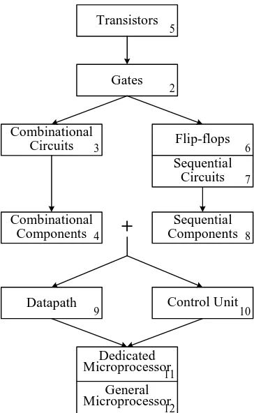
Irregardless of whether a circuit is combinational or sequential, they are all made up of the three basic logic gates: AND, OR, and NOT gates. From these three basic gates, the most powerful computer can be made. Furthermore, these basic gates are built using transistors — the fundamental building blocks for all digital logic circuits. Transistors are just electronic binary switches that can be turned on or off. The on and off states of a transistor are used to represent the two binary values: 1 and 0.
Combinational
Circuits Flip-flops
Sequential Components Combinational
Components
Datapath Control Unit
Gates Transistors
+
5
2
3
4
6
8
9 10
11
Dedicated Microprocessor
12
General Microprocessor
[image:19.612.214.396.70.366.2]Sequential Circuits 7
Figure 1.3. Summary of how the parts of a microprocessor fit together. The numbers in each box denote the chapter number in which the topic is discussed.
1.2 Design Abstraction Levels
Digital circuits can be designed at any one of several abstraction levels. When designing a circuit at the transistor level, which is the lowest level, you are dealing with discrete transistors and connecting them together to form the circuit. The next level up in the abstraction is the gate level. At this level, you are working with logic gates to build the circuit. At the gate level, you also can specify the circuit using either a truth table or a Boolean equation. In using logic gates, a designer usually creates standard combinational and sequential components for building larger circuits. In this way, a very large circuit, such as a microprocessor, can be built in a hierarchical fashion. Design methodologies have shown that solving a problem hierarchically is always easier than trying to solve the entire problem as a whole from the ground up. These combinational and sequential components are used at the register-transfer level in building the datapath and the control unit in the microprocessor. At the register-transfer level, we are concerned with how the data is transferred between the various registers and functional units to realize or solve the problem at hand. Finally, at the highest level, which is the behavioral level, we construct the circuit by describing the behavior or operation of the circuit using a hardware description language. This is very similar to writing a computer program using a programming language.
1.3 Examples of a 2-to-1 Multiplexer
As an example, let us look at the design of the 2-to-1 multiplexer from the different abstraction levels. At this point, don’t worry too much if you don’t understand the details of how all of these circuits are built. This is intended just to give you an idea of what the description of the circuits look like at the different abstraction levels. We will get to the details in the rest of the book.
(how much it costs to manufacture), and power usage (how much power it uses). Hence, when designing a circuit, besides being functionally correct, there will always be economic versus performance tradeoffs that we need to consider.
The multiplexer is a component that is used a lot in the datapath. An analogy for the operation of the 2-to-1 multiplexer is similar in principle to a railroad switch in which two railroad tracks are to be merged onto one track. The switch controls which one of the two trains on the two separate tracks will move onto the one track. Similarly, the 2-to-1 multiplexer has two data inputs, d0 and d1, and a select input, s. The select input determines which data
from the two data inputs will pass to the output, y.
Figure 1.4 shows the graphical symbol also referred to as the logic symbol for the 2-to-1 multiplexer. From looking at the logic symbol, you can tell how many signal lines the 2-to-1 multiplexer has, and the name or function designated for each line. For the 2-to-1 multiplexer, there are two data input signals, d1 and d0, a select input signal,
s, and an output signal, y.
y d1 d0
s 1 0
Figure 1.4. Logic symbol for the 2-to-1 multiplexer.
1.3.1 Behavioral
Level
We can describe the operation of the 2-to-1 multiplexer simply, using the same names as in the logic symbol, by saying that
d0 passes to y when s = 0, and
d1 passes to y when s = 1
Or more precisely, the value that is at d0 passes to y when s = 0, and the value that is at d1 passes to y when s = 1.
We use a hardware description language (HDL) to describe a circuit at the behavioral level. When describing a circuit at this level, you would write basically the same thing as in the description, except that you have to use the correct syntax required by the hardware description language. Figure 1.5 shows the description of the 2-to-1 multiplexer using the hardware description language called VHDL.
LIBRARY ieee;
USE ieee.std_logic_1164.ALL;
ENTITY multiplexer IS PORT ( d0, d1, s: IN STD_LOGIC; y: OUT STD_LOGIC);
END multiplexer;
ARCHITECTURE Behavioral OF multiplexer IS BEGIN
PROCESS(s, d0, d1) BEGIN
y <= d0 WHEN s = '0' ELSE d1; END PROCESS;
END Behavioral;
Figure 1.5. Behavioral level VHDL description of the 2-to-1 multiplexer.
interface for the circuit by specifying the input and output signals of the circuit. In this example, there are three input signals of type STD_LOGIC, and one output signal also of type STD_LOGIC. The ARCHITECTURE section defines the actual operation of the circuit. The operation of the multiplexer is defined in the one conditional signal assignment statement
y <= d0 WHEN s = '0' ELSE d1;
The statement, which uses the symbol <= to denote the signal assignment, says that the signal y gets the value of d0
when s is equal to 0, otherwise, y gets the value of d1.
As you can see, when designing circuits at the behavioral level, we do not need to know what logic gates are needed or how they are connected together. We only need to know their interface and operation.
1.3.2 Gate
Level
At the gate level, you can draw a schematic diagram, which is a diagram showing how the logic gates are connected together. Two schematic diagrams of a circuit are shown in Figure 1.6(a) and (b). In Figure 1.6(a), the circuit uses three inverters ( ), four 3-input AND gates ( ), and one 4-input OR gate ( ). In Figure 1.6(b), only one inverter, two 2-input AND gates, and one 2-input OR gate are needed. Although one circuit is larger (in terms of the number of gates needed) than the other, both of these circuits realize the same 2-to-1 multiplexer function. Therefore, when we want to actually implement a 2-to-1 multiplexer circuit, we will want to use the second, smaller circuit rather than the first.
d0 d1 s
y
(a)
d0
d1
s y
(b)
Figure 1.6. Gate level circuit diagram for the 2-to-1 multiplexer: (a) circuit using eight gates; (b) circuit using four gates.
At the gate level, you can also describe the 2-to-1 multiplexer using a truth table or with a Boolean equation as shown in Figure 1.7(a) and (b) respectively. For the truth table, we list all possible combinations of the binary values for the three inputs s, d0 and d1, and then determine what the output value y should be based on the functional
description of the circuit. We see that for the first four rows of the table when s = 0, y has the same values as d0,
whereas in the last four rows when s = 1, y has the same values as d1.
The Boolean equation in (b) can be derived from either the schematic diagram or the truth table. The first equality in (b) matches the truth table in (a), and also the schematic diagram in Figure 1.6(a). The second equality in (b) matches the schematic diagram in Figure 1.6(b). To derive the equation from the truth table, we look at all the rows where the output y is a 1. Each of these rows results in a term in the equation. For each term, the variable is primed (' ) when the value of the variable is a 0, and unprimed when the value of the variable is a 1.
s d1 d0 y
0 0 0 0 0 0 1 1 0 1 0 0 0 1 1 1 1 0 0 0
y = s' d1' d0 + s' d1 d0 + s d1 d0' + s d1 d0
1 0 1 0 1 1 0 1 1 1 1 1
(a)
(b)
Figure 1.7. Gate level description of the 2-to-1 multiplexer: (a) using a truth table; (b) using a Boolean equation.
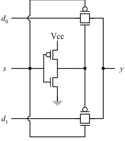
1.3.3 Transistor
Level
The 2-to-1 multiplexer circuit at the transistor level is shown in Figure 1.8. It contains six transistors, three of which are PMOS ( ), and three are NMOS ( ). The pair of transistors on the left forms an inverter for the signal s, while the two pairs of transistors on the right form two transmission gates. The transmission gate allows or disallows the data signal d0 or d1 to pass through, depending on the control signal s. The top transmission gate is
turned on when s is a 0, and the bottom transmission gate is turned on when s is a 1. Hence, when s is 0, the value at d0 is passed to y, and when s is 1, the value at d1 is passed to y.
Vcc
s y
d0
[image:22.612.244.367.275.414.2]d1
Figure 1.8. Transistor circuit for the 2-to-1 multiplexer.
1.4 Introduction to VHDL
The popularity of using hardware description languages (HDL) for designing digital circuits began in the mid-1990s when commercial synthesis tools became available. Two popular HDLs used by many engineers today are VHDL and Verilog. VHDL, which stands for VHSIC Hardware Description Language, and VHSIC, in turn, stands for Very High Speed Integrated Circuit, was jointly sponsored and developed by the U.S. Department of Defense and the IEEE in the mid-1980s. It was standardized by the IEEE in 1987 (VHDL-87), and later extended in 1993 (VHDL-93). Verilog, on the other hand, was first introduced in 1984, and later in 1988, as a proprietary hardware description language by the two companies Synopsys and Cadence Design Systems. In this book, we will use VHDL.
VHDL, in many respects, is similar to a regular computer programming language, such as C++. For example, it has constructs for variable assignments, conditional statements, loops, and functions, just to name a few. In a computer programming language, a compiler is used to translate the high-level source code to machine code. In VHDL, however, a synthesizer is used to translate the source code to a description of the actual hardware circuit that implements the code. From this description, which we call a netlist, the actual physical digital device that realizes the source code can be made automatically. Accurate functional and timing simulation of the code is also possible in order to test the correctness of the circuit.
no PROCESS statement. Statements within a PROCESS block are executed sequentially like in a computer program, while statements outside a PROCESS block (including the PROCESS block itself) are executed concurrently or in parallel. The signal assignment statement, using the symbol <=, is derived directly from the Boolean equation for the multiplexer as shown in Figure 1.7(b) using the built-in VHDL operators AND, OR, and NOT.
LIBRARY ieee;
USE ieee.std_logic_1164.ALL;
ENTITY multiplexer IS PORT( d0, d1, s: IN STD_LOGIC; y: OUT STD_LOGIC);
END multiplexer;
ARCHITECTURE Dataflow OF multiplexer IS BEGIN
y <= ((NOT s) AND d0) OR (s AND d1); END Dataflow;
Figure 1.9. Dataflow level VHDL description of the 2-to-1 multiplexer.
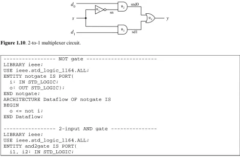
In addition to the behavioral and dataflow levels, we can also write VHDL code at the structural level. Figure 1.11 shows the VHDL code for the multiplexer written at the structural level. The code is based on the circuit shown in Figure 1.10. The three different gates (and2gate, or2gate, and notgate) used in the circuit are first declared and defined using the ENTITY and ARCHITECTURE statements respectively. After this, the multiplexer is declared, also with the ENTITY statement. The actual structural definition of the multiplexer is in the ARCHITECTURE section for multiplexer2. First of all, the COMPONENT statements specify what components are used in the circuit. The SIGNAL
statement declares three internal signals that will be used in the connection of the circuit. Finally, the PORT MAP
statements declare the instances of the gates used in the circuit, and also specify how they are connected using the external and internal signals.
snd0 sn
sd1 u2
u3 u1
u4 d0
d1
[image:23.612.71.540.413.724.2]s y
Figure 1.10. 2-to-1 multiplexer circuit.
--- NOT gate ---LIBRARY ieee;
USE ieee.std_logic_1164.ALL; ENTITY notgate IS PORT(
i: IN STD_LOGIC; o: OUT STD_LOGIC); END notgate;
ARCHITECTURE Dataflow OF notgate IS BEGIN
o <= not i; END Dataflow;
-- 2-input AND gate ---LIBRARY ieee;
USE ieee.std_logic_1164.ALL; ENTITY and2gate IS PORT(
o: OUT STD_LOGIC); END and2gate;
ARCHITECTURE Dataflow OF and2gate IS BEGIN
o <= i1 AND i2; END Dataflow;
- 2-input OR gate ---LIBRARY ieee;
USE ieee.std_logic_1164.ALL; ENTITY or2gate IS PORT(
i1, i2: IN STD_LOGIC; o: OUT STD_LOGIC); END or2gate;
ARCHITECTURE Dataflow OF or2gate IS BEGIN
o <= i1 OR i2; END Dataflow;
--- 2-to-1 multiplexer ---LIBRARY ieee;
USE ieee.std_logic_1164.ALL; ENTITY multiplexer IS PORT(
d0, d1, s: IN STD_LOGIC; y: OUT STD_LOGIC);
END multiplexer;
ARCHITECTURE Structural OF multiplexer IS COMPONENT notgate PORT(
i: IN STD_LOGIC; o: OUT STD_LOGIC); END COMPONENT;
COMPONENT and2gate PORT( i1, i2: IN STD_LOGIC; o: OUT STD_LOGIC); END COMPONENT;
COMPONENT and3gate PORT( i1, i2, i3: IN STD_LOGIC; o: OUT STD_LOGIC);
END COMPONENT;
COMPONENT or2gate PORT( i1, i2: IN STD_LOGIC; o: OUT STD_LOGIC); END COMPONENT;
SIGNAL sn, snd0, sd1: STD_LOGIC;
BEGIN
U1: notgate PORT MAP(s,sn);
U2: and2gate PORT MAP(d0, sn, snd0); U3: and2gate PORT MAP(d1, s, sd1); U4: or2gate PORT MAP(snd0, sd1, y); END Structural;
1.5 Synthesis
Given a gate level circuit diagram, such as the one shown in Figure 1.6, you can actually get some discrete logic gates, and manually connect them together with wires on a breadboard. Traditionally, this is how electronic engineers actually designed and implemented digital logic circuits. However, this is not how electronic engineers design circuits anymore. They write programs, such as the one in Figure 1.5, just like what computer programmers do. The question then is how does the program that describes the operation of the circuit actually get converted to the physical circuit?
The problem here is similar to translating a computer program written in a high-level language to machine language for a particular computer to execute. For a computer program, we use a compiler to do the translation. For translating a digital logic circuit, we use a synthesizer. Instead of using a high-level computer language to describe a computer program, we use a hardware description language (HDL) to describe the operations of a digital logic circuit. Writing a description of a digital logic circuit is similar to writing a computer program; the only difference is that a different language is used. A synthesizer is then used to translate the HDL program into the circuit netlist. A netlist is a description of how a circuit is actually realized or connected using basic gates. This translation process from a HDL description of a circuit to its netlist is referred to as synthesis.
Furthermore, the netlist from the output of the synthesizer can be used directly to implement the actual circuit in a programmable logic device (PLD) chip such as a field programmable gate array (FPGA). With this final step, the creation of a digital circuit that is fully implemented in an integrated circuit (IC) chip can be easily done. The Appendix gives a tutorial of the complete process from writing the VHDL code to synthesizing the circuit and uploading the netlist to the FPGA chip using Altera’s development system.
1.6 Going
Forward
[image:25.612.155.456.469.696.2]We will now embark upon a journey that will take you from a simple transistor to the building of a microprocessor. Figure 1.2 will serve as our guide and map. If you get lost on the way, and do not know where a particular component fits in the overall picture, just refer to this map. At the beginning of each chapter, I will refresh your memory with this map by highlighting the components in the map that the chapter will cover.
Figure 1.12 is an actual picture of the circuitry inside an Intel Pentium 4 CPU. When you reach the end of this book, you still may not be able to design the circuit for the P4, but you will certainly have the knowledge of how a microprocessor is designed because you will actually have designed and implemented a working microprocessor yourself.
1.7 Summary
Checklist
Microprocessor
General-purpose microprocessor Dedicated microprocessor, ASIC Datapath
Control unit
Finite state machine (FSM) Next-state logic
State memory Output logic
Combinational circuit Sequential circuit Transistor level design Gate level design
Register-transfer level design Behavioral level design Logic symbol
VHDL Synthesis Netlist
1.8 Problems
1.1. Find out the approximate number of general-purpose microprocessors sold in the US in a year versus the number of dedicated microprocessors sold.
1.2. Compile a list of devices that you use during one regular day that are controlled by a microprocessor.
1.3. Describe what your regular daily routine will be like if there is no electrical power, including battery power, available.
1.4. Apply the Von Neumann model of a computer system as shown in Figure 1.1 to the following systems. Determine what parts of the system correspond to the different parts of the model.
a) Traffic light b) Heart pace maker c) Microwave oven d) Musical greeting card
e) Hard disk drive (not the entire personal computer)
1.5. The speed of a microprocessor is often measured by its clock frequency. What is the clock frequency of the fastest general-purpose microprocessor available?
1.6. Compare some typical clock speeds between general-purpose microprocessors versus dedicated microprocessors.
1.7. Summarize the mainstream generations of the Intel general-purpose microprocessors used in personal computers starting with the 8086 CPU. List the year introduced, the clock speed, and the number of transistors in each.
CPU Year Introduced Clock Speed Number of Transistors
8086 1978 4.7 – 10 MHz 29,000
80286 1982 6 – 12 MHz 134,000
80386 1985 16 – 33 MHz 275,000
80486 1989 25 – 100 MHz 1.2 million
Pentium 1993 60 – 200 MHz 3.3 million
Pentium Pro 1995 150 – 200 MHz 5.5 million Pentium II 1997 234 – 450 MHz 7.5 million
Celeron 1998 266 – 800 MHz 19 million
Pentium III 1999 400 MHz – 1.2 GHz 28 million
Pentium 4 2000 1.4 – 3 GHz 42 million
1.8. Using Figure 1.9 as a template, write the dataflow VHDL code for the 2-to-1 multiplexer circuit shown in Figure 1.6(a).
1.9. Using Figure 1.11 as a template, write the structural VHDL code for the 2-to-1 multiplexer circuit shown in Figure 1.6(a).
Digital Circuits
Control Signals
Status Signals
MUX
'0'
Data Inputs
Data Outputs
Datapath
ALU Register
ff
8
8 8
Output Logic
Next-state Logic
Control Inputs
Control Outputs
State Memory Register
Control Unit
Our world is an analog world. Measurements that we make of the physical objects around us are never in discrete units, but rather in a continuous range. We talk about physical constants such as 2.718281828… or 3.141592…. To build analog devices that can process these values accurately is next to impossible. Even building a simple analog radio requires very accurate adjustments of frequencies, voltages, and currents at each part of the circuit. If we were to use voltages to represent the constant 3.14, we would have to build a component that will give us exactly 3.14 volts every time. This is again impossible; due to the imperfect manufacturing process, each component produced is slightly different from the others. Even if the manufacturing process can be made as perfect as perfect can get, we still would not be able to get 3.14 volts from this component every time we use it. The reason being that the physical elements used in producing the component behave differently in different environments, such as temperature, pressure, and gravitational force, just to name a few. Therefore, even if the manufacturing process is perfect, using this component in different environments will not give us exactly 3.14 volts every time.
To make things simpler, we work with a digital abstraction of our analog world. Instead of working with an infinite continuous range of values, we use just two values! Yes, just two values: 1 and 0, on and off, high and low, true and false, black and white, or however you want to call it. It is certainly much easier to control and work with two values rather than an infinite range. We call these two values a binary value for the reason that there are only two of them. A single 0 or a single 1 is then a binary digit or bit. This sounds great, but we have to remember that the underlining building block for our digital circuits is still based on an analog world.
This chapter provides the theoretical foundations for building digital logic circuits using logic gates, the basic building blocks for all digital circuits. In order to understand how logic gates are used to implement digital circuits, we need to have a good understanding of the basic theory of Boolean algebra, Boolean functions, and how to use and manipulate them. Most people may find Sections 2.5 and 2.6 on these theories to be boring, but let me encourage you to grind through it patiently, because if you do not understand it now, you will quickly get lost in the later chapters. The good news is that these two sections are the only sections in this book on theory, and I will try to keep it as short and simple as possible. You will also find that many of the Boolean Theorems are very familiar, because they are similar to the Algebra Theorems that you have learned from your high school math class. As you can see from the microprocessor road map, this chapter affects all the parts for building a microprocessor.
2.1 Binary
Numbers
Since digital circuits deal with binary values, we will begin with a quick introduction to binary numbers. A bit, having either the value of 0 or 1, can represent only two things or two pieces of information. It is, therefore, necessary to group many bits together to represent more pieces of information. A string of n bits can represent 2n different pieces of information. For example, a string of two bits results in the four combinations 00, 01, 10, and 11. By using different encoding techniques, a group of bits can be used to represent different information, such as a number, a letter of the alphabet, a character symbol, or a command for the microprocessor to execute.
The use of decimal numbers is quite familiar to us. However, since the binary digit is used to represent information within the computer, we also need to be familiar with binary numbers. Note that the use of binary numbers is just a form of representation for a string of bits. We can just as well use octal, decimal, or hexadecimal numbers to represent the string of bits. In fact, you will find that hexadecimal numbers are often used as a shorthand notation for binary numbers.
The decimal number system is a positional system. In other words, the value of the digit is dependent on the position of the digit within the number. For example, in the decimal number 48, the decimal digit 4 has a greater value than the decimal digit 8 because it is in the tenth position, whereas the digit 8 is in the unit position. The value of the number is calculated as 4×101 + 8×100.
Like the decimal number system, the binary number system is also a positional system. The only difference between the two is that the binary system is a base-2 system, and so it uses only two digits, 0 and 1, instead of ten. The binary numbers from 0 to 15 (decimal) are shown in Figure 2.1. The range from 0 to 15 has 16 different combinations. Since 24 = 16, therefore, we need a 4-bit binary number, i.e., a string of four bits, to represent this range.
The decimal value of a binary number can be found just like for a decimal number except that we raise the base number 2 to a power rather than the base number 10 to a power. For example, the value for the decimal number 658 is
65810 = 6×10² + 5×101 + 8×100 = 600 + 50 + 8 = 65810
Similaly, the decimal value for the binary number 10110112 is
10110112 = 1×26 + 0×25 + 1×24 + 1×23 + 0×22 + 1×21 + 1×20 = 64 + 16 + 8 + 2 + 1 = 9110
To get the decimal value, the least significant bit (in this case, the rightmost 1) is multiplied with 20. The next bit to the left is multiplied with 21, and so on. Finally, they are all added together to give the value 9110.
Notice the subscript 10 in the decimal number 65810, and the 2 in the binary number 10110112. This subscript is
used to denote the base of the number whenever there might be confusion as to what base the number is in. Decimal Binary Octal Hexadecimal
0 0000 0 0
1 0001 1 1
2 0010 2 2
3 0011 3 3
4 0100 4 4
5 0101 5 5
6 0110 6 6
7 0111 7 7
8 1000 10 8
9 1001 11 9
10 1010 12 A
11 1011 13 B
12 1100 14 C
13 1101 15 D
14 1110 16 E
15 1111 17 F
Figure 2.1 Numbers from 0 to 15 in binary, octal, and hexadecimal.
Converting a decimal number to its binary equivalent can be done by successively dividing the decimal number by 2 and keeping track of the remainder at each step. Combining the remainders together (starting with the last one) forms the equivalent binary number. For example, using the decimal number 91, we divide it by 2 to get 45 with a remainder of 1. Then we divide 45 by 2 to get 22 with a remainder of 1. We continue in this fashion until the end as shown below.
91 2
45 1 2
22 1 2
11 0 2
5 1 2
2 1 2
1 0
most significant bit least significant bit
= 1011011
Concatenating the remainders together starting with the last one results in the binary number 10110112.
Octal numbers only use the digits from 0 to 7 for the eight different combinations. When counting in octal, the number after 7 is 10 as shown in Figure 2.1. To convert a binary number to octal, we simply group the bits into groups of threes starting from the right. The reason for this is because 8 = 23. For each group of three bits, we write the equivalent octal digit for it. For example, the conversion of the binary number 1 110 0112 to the octal number
1638 is shown below.
001 110 011 1 6 3
Since the original binary number has seven bits, we need to extend it with two leading zeros to get three bits for the leftmost group. Note that when we are dealing with negative numbers, we may require extending the number with leading ones instead of zeros.
Converting an octal number to its binary equivalent is just as easy. For each octal number, we write down the equivalent three bits. These groups of three bits are concatenated together to form the final binary number. For example, the conversion of the octal number 57248 to the binary number 101 111 010 1002 is shown below.
5 7 2 4 101 111 010 100
The decimal value of an octal number can be found just like for a binary or decimal number except that we raise the base number 8 to a power instead. For example, the octal number 57248 has the value
57248 = 5×83 + 7×82 + 2×81 + 4×80 = 2560 + 448 + 16 + 4 = 302810
Hexadecimal numbers are treated basically the same way as octal numbers except with the appropriate changes to the base. Hexadecimal (or hex for short) numbers use base-16, and thus require 16 different digit symbols as shown in Figure 2.1. Converting binary numbers to hexadecimal numbers involve grouping the bits into groups of fours since 16 = 24. For example, the conversion of the binary number 110 1101 10112 to the hexadecimal number
6DB16 is shown below. Again, we need to extend it with a leading zero to get four bits for the leftmost group.
0110 1101 1011
6 D B
To convert a hex number to a binary number, we write down the equivalent four bits for each hex digit, and then concatenate them together to form the final binary number. For example, the conversion of the hexadecimal number 5C4A16 to the binary number 0101 1100 0100 10102 is shown below.
5 C 4 A 0101 1100 0100 1010
The following example shows how the decimal value of the hexadecimal number C4A16 is evaluated.
C4A16 = C×162 + 4×161 + A×160 = 12×162 + 4×161 + 10×160 = 3072 + 64 + 10 = 314610
2.2 Binary
Switch
in out in out
(a) (b)
control
Figure 2.2 Binary switch: (a) opened or off; (b) closed or on.
Uses of the binary switch idea can be found in many real world devices. For example, the switch can be an electrical switch with the input connected to a power source and the output connected to a siren S as shown in Figure 2.3.
Battery Siren
Switch
Figure 2.3 A siren controlled by a switch.
When the switch is closed, the siren turns on. The usual convention is to use a 1 to mean “on” and a 0 to mean “off.” Therefore, when the switch is closed, the output is a 1 and the siren will turn on. We can also use a variable, x, to denote the state of the switch. We can let x = 1 to mean the switch is closed and x = 0 to mean the switch is opened. Using this convention, we can describe the state of the siren S in terms of the variable x using a simple logic expression. Since S = 1 if x = 1 and S = 0 if x = 0, we can write
S = x
This logic expression describes the output S in terms of the input variable x.
2.3 Basic Logic Operators and Logic Expressions
Two binary switches can be connected together either in series or in parallel as shown in Figure 2.4.
(b)
F
(a)
F
x
y y
x
Figure 2.4 Connection of two binary switches: (a) in series; (b) in parallel.
If two switches are connected in series as in (a), then both switches have to be on in order for the output F to be a 1. In other words, F = 1 if x = 1 ANDy = 1. If either x or y is off, or both are off, then F = 0. Translating this into a logic expression, we get
F = xANDy
Hence, two switches connected in series give rise to the logical AND operator. In a Boolean function (which we will explain in more detail in section 2.5) the AND operator is either denoted with a dot ( • ) or no symbol at all. Thus we can rewrite the above expression as
F = xy
If we connect two switches in parallel as in (b), then only one switch needs to be on in order for the output F to be a 1. In other words, F = 1 if either x = 1, or y = 1, or both x and y are 1’s. This means that F = 0 only if both x and y are 0’s. Translating this into a logic expression, we get
F = xORy
and this gives rise to the logical OR operator. In a Boolean function, the OR operator is denoted with a plus symbol ( + ). Thus we can rewrite the above expression as
F = x + y
In addition to the AND and OR operators, there is another basic logic operator – the NOT operator, also known as the INVERTER. Whereas, the AND and OR operators have multiple inputs, the NOT operator has only one input and one output. The NOT operator simply inverts its input, so a 0 input will produce a 1 output, and a 1 becomes a 0. In a Boolean function, the NOT operator is either denoted with an apostrophe symbol ( ' ) or a bar on top ( ) as in
F = x'
or
x F=
When several operators are used in the same expression, the precedence given to the operators are, from highest
to lowest, NOT, AND, and OR. The order of evaluation can be changed by means of using parenthesis. For example,
the expression
F = xy + z'
means (x and y) or (not z), and the expression
F = x(y + z)'
means x and (not (y or z)).
2.4 Truth
Tables
The operation of the AND, OR, and NOT logic operators can be formally described by using a truth table as
shown in Figure 2.5. A truth table is a two-dimensional array where there is one column for each input and one column for each output (a circuit may have more than one output). Since we are dealing with binary values, each input can be either a 0 or a 1. We simply enumerate all possible combinations of 0’s and 1’s for all the inputs.
Usually, we want to write these input values in the normal binary counting order. With two inputs, there are 22
combinations giving us the four rows in the table. The values in the output column are determined from applying the
corresponding input values to the functional operator. For the AND truth table in Figure 2.5(a), F = 1 only when x
and y are both 1, otherwise, F = 0. For the OR truth table (b), F = 1 when either x or y or both is a 1, otherwise F = 0. For the NOT truth table, the output F is just the inverted value of the input x.
x y F
0 0 0 0 1 0 1 0 0 1 1 1
(a)
x y F
0 0 0 0 1 1 1 0 1 1 1 1
(b)
x F
0 1 1 0
(c)
Figure 2.5 Truth tables for the three basic logical operators: (a) AND; (b) OR; (c) NOT.
to describe digital circuits are given in the following sections. Another method to formally describe the operation of a circuit is by using Boolean expressions or Boolean functions.
2.5 Boolean Algebra and Boolean Function
2.5.1 Boolean
Algebra
George Boole, in 1854, developed a system of mathematical logic, which we now call Boolean algebra. Based
on Boole’s idea, Claude Shannon, in 1938, showed that circuits built with binary switches can easily be described using Boolean algebra. The abstraction from switches being on and off to the use of Boolean algebra is as follows.
Let B = {0, 1} be the Boolean algebra whose elements are one of the two values, 0 and 1. We define the operations
AND (•), OR (+), and NOT (' ) for the elements of B by the axioms in Figure 2.6(a). These axioms are simply the
definitions for the AND, OR, and NOT operators.
A variable x is called a Boolean variable if x takes on only values in B, i.e. either 0 or 1. Consequently, we
obtain the theorems in Figure 2.6(b) for single variable and Figure 2.6(c) for two and three variables.
Theorems in Figure 2.6(b) can be proved easily by substituting the binary values into the expressions and using
the axioms. For example, to show that Theorem 6a is true, we substitute 0 into x to get axiom 3a, and substitute 1
into x to get axiom 2a.
To prove the theorems in Figure 2.6(c), we can use either one of two methods: 1) use a truth table, or 2) use axioms and theorems that have already been proven. We show these two methods in the following two examples.
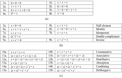
1a. 0 • 0 = 0 1b. 1 + 1 = 1
2a. 1 • 1 = 1 2b. 0 + 0 = 0
3a. 0 • 1 = 1 • 0 = 0 3b. 1 + 0 = 0 + 1 = 1
4a. 0' = 1 4b. 1' = 0
(a)
5a. x• 0 = 0 5b. x + 1 = 1 Null element
6a. x• 1 = 1 •x = x 6b. x + 0 = 0 + x = x Identity
7a. x• x = x 7b. x + x = x Idempotent
8a. (x' )' = x Double complement
9a. x•x' = 0 9b. x + x' = 1 Inverse
(b)
10a. x•y = y•x 10b. x + y = y + x Commutative
11a. (x•y) •z = x • (y •z) 11b. (x + y) + z = x + (y + z) Associative
12a. x• (y + z) = (x•y) + (x•z) 12b. x + (y•z) = (x + y) • (x + z) Distributive
13a. x• (x + y) = x 13b. x + (x•y) = x Absorption
14a. (x •y)+ (x •y' ) = x 14b. (x +y)• (x + y' ) = x Combining
15a. (x•y)' = x' + y' 15b. (x + y)' = x'•y' DeMorgan’s
[image:34.612.83.510.335.608.2](c)
Figure 2.6 Boolean algebra axioms and theorems: (a) Axioms; (b) Single variable theorems; (c) two and three variable theorems.
Example 2.1: Proof of theorem using a truth table.
Theorem 12a states that x• (y + z) = (x•y) + (x•z). To prove that Theorem 12a is true using a truth table, we
need to show that for every combination of values for the three variables x, y, and z, the left-hand side of the
x y z (y + z) (x•y) (x•z) x• (y + z) (x•y) + (x•z)
0 0 0 0 0 0 0 0
0 0 1 1 0 0 0 0
0 1 0 1 0 0 0 0
0 1 1 1 0 0 0 0
1 0 0 0 0 0 0 0
1 0 1 1 0 1 1 1
1 1 0 1 1 0 1 1
1 1 1 1 1 1 1 1
We start with the first three columns labeled x, y, and z, and enumerate all possible combinations of values for
these three variables. For each combination (row), we evaluate the intermediate expressions y+z, x•y, and x•z by
substituting the values of x, y, and z into the expression. Finally, we obtain the values for the last two columns,
which correspond to the left-hand side and right-hand side of Theorem 12a. The values in these two columns are
identical for every combination of x, y, and z, therefore, we can say that Theorem 12a is true. ♦
Example 2.2: Proof of theorem using axioms and theorems.
Theorem 13b states that x + (x•y) = x. To prove that Theorem 13b is true using axioms and theorems, we can
argue as follows:
x + (x •y) = (x • 1) + (x •y) by Identity Theorem 6a
= x• (1 + y) by Distributive Theorem 12a
= x• (1) by Null element Theorem 5b
= x by Identity Theorem 6a ♦
Example 2.2 shows that some theorems can be derived from others that have already been proven with the truth table. Full treatment of Boolean algebra is beyond the scope of this book and can be found in the references. For our purposes, we simply assume that all the theorems are true and will just use them to show that two circuits are equivalent as depicted in the next two examples.
Example 2.3: Use Boolean algebra to reduce the equation F(x,y,z) = (x' + y' + x'y' + xy) (x' + yz) as much as possible.
F = (x' + y' + x'y' + xy) (x' + yz)
= (x' • 1+ y' • 1 + x'y' + xy) (x' + yz) by Identity Theorem 6a
= (x' (y + y' )+ y' (x + x' ) + x'y' + xy) (x' + yz) by Inverse Theorem 9b = (x'y + x'y' + y'x + y'x' + x'y' + xy) (x' + yz) by Distributive Theorem 12a
= (x'y + x'y' + y'x + y'x' + x'y' + xy) (x' + yz) by Idempotent Theorem 7b
= (x' (y + y')+ x (y + y')) (x' + yz) by Distributive Theorem 12a
= (x' • 1+ x • 1) (x' + yz) by Inverse Theorem 9b
= (x' + x) (x' + yz) by Identity Theorem 6a
= 1 (x' + yz) by Inverse Theorem 9b
= (x' + yz) by Identity Theorem 6a
Since the expression (x' + y' + x'y' + xy) (x' + yz) reduces down to (x' + yz), therefore, we do want to implement
the circuit for the latter expression rather then the former because the circuit size for the latter is much smaller. ♦
Example 2.4: Show, using Boolean algebra, that the two equations F1 = (xy' + x'y + x' + y' + z' ) (x + y' + z) and
F2 = y' + x'z + xz' are equivalent.
F1 = (xy' + x'y + x' + y' + z' ) (x + y' + z)
= xy'x + xy'y' + xy'z + x'yx + x'yy' + x'yz + x'x + x'y' + x'z + y'x + y'y' + y'z + z'x + z'y' + z'z
= xy' + xy' + xy'z + 0 +0 + x'yz + 0 + x'y' + x'z + xy' + y' + y'z + xz' + y'z' + 0 = xy' + xy'z + x'yz + x'y' + x'z + y' + y'z + xz' + y'z'