This is a repository copy of
Coulomb blockade directional coupler
.
White Rose Research Online URL for this paper:
http://eprints.whiterose.ac.uk/88071/
Version: Accepted Version
Article:
Pingue, P., Piazza, V., Beltram, F. et al. (3 more authors) (2005) Coulomb blockade
directional coupler. Applied Physics Letters, 86. 052102 . ISSN 0003-6951
https://doi.org/10.1063/1.1857078
eprints@whiterose.ac.uk https://eprints.whiterose.ac.uk/
Reuse
Unless indicated otherwise, fulltext items are protected by copyright with all rights reserved. The copyright exception in section 29 of the Copyright, Designs and Patents Act 1988 allows the making of a single copy solely for the purpose of non-commercial research or private study within the limits of fair dealing. The publisher or other rights-holder may allow further reproduction and re-use of this version - refer to the White Rose Research Online record for this item. Where records identify the publisher as the copyright holder, users can verify any specific terms of use on the publisher’s website.
Takedown
If you consider content in White Rose Research Online to be in breach of UK law, please notify us by
arXiv:cond-mat/0412507v1 [cond-mat.mes-hall] 18 Dec 2004
P. Pingue,1,∗ V. Piazza,1 F. Beltram,1 I. Farrer,2 D.A. Ritchie,2 and M. Pepper2
1
NEST-INFM & Scuola Normale Superiore, I-56126 Pisa, Italy 2
Cavendish Laboratory, University of Cambridge, Madingley Road, Cambridge CB3 0HE, United Kingdom
A tunable directional coupler based on Coulomb Blockade effect is presented. Two electron waveg-uides are coupled by a quantum dot to an injector waveguide. Electron confinement is obtained by surface Schottky gates on single GaAs/AlGaAs heterojunction. Magneto-electrical measurements down to 350 mK are presented and large transconductance oscillations are reported on both out-puts up to 4.2 K. Experimental results are interpreted in terms of Coulomb Blockade effect and the relevance of the present design strategy for the implementation of an electronic multiplexer is underlined.
PACS numbers: 73.23.Ad, 73.23.Hk, 73.63.Nm
Controlled directional injection of electrons from one electronic waveguide to another is being intensively in-vestigated owing to its importance in wavelength multi-plexing and in telecommunication routing devices. While photonic multiplexers represent a mature technology, electronic steering devices are still at their infancy.
Pioneering designs were demonstrated exploiting a field-effect tunable barrier between two semiconductor waveguides [1, 2, 3, 4, 5], implementing a Y-branch switch or switching the electrons by means of elec-tric side-gates[6, 7, 8]. An electronic device based on two electron waveguides coupled by an open interac-tion window rather than a tunneling barrier was also proposed[9, 10, 11] and realized[12], but so far no switch-ing behavior was demonstrated in this configuration.
In this Letter we describe a scheme where the coupling element between two semiconductor waveguides is a sin-gle quantum dot (QD) and Coulomb blockade (CB) gov-erns electron routing. We shall demonstrate that in the classic configuration with two electron waveguides mix-ing at an open ballistic window a QD can be induced – with appropriate biasing conditions and geometry – and employed as a gate-controlled coupling element between the two waveguides.
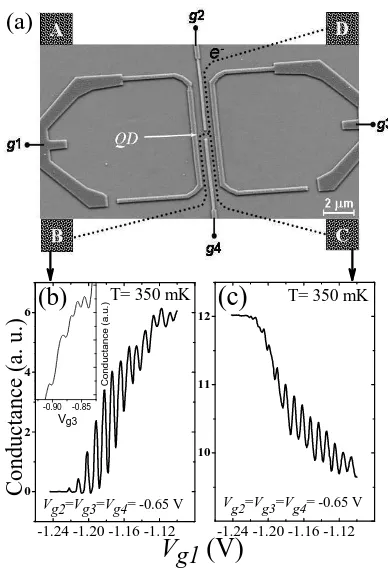
Figure 1(a) shows a scanning electron microscope (SEM) picture of the device. Schottky gates are la-beled g1 through g4. The Al split-gate structure was nanofabricated by e-beam lithography and thermal evap-oration. The waveguides of the device described in this work have a total length L = 7.5 µm each and a ge-ometrical width W = 0.44 µm. The central split-gate is w = 0.17 µm wide while the coupling window is
l = 0.57 µm long. The GaAs/AlGaAs heterostructure contains a two-dimensional electron gas (2DEG) located 70 nm below the surface with a mobility ofµ= 3.7×10⁵
cm2/Vs and a carrier concentration ofn= 2.4
×1011cm−2
at 350 mK.
In our experiment gatesg2tog4were negatively biased
∗Electronic address: pingue@sns.it
-1.24 -1.20 -1.16 -1.12 10
11 12
-1.24 -1.20 -1.16 -1.12 0
2 4 6
T= 350 mK
Vg2=Vg3=Vg4= -0.65 V T= 350 mK
V
g1
(V)
-0.90 -0.85
C
o
n
d
u
c
ta
n
c
e
(
a
.u
.)
Vg3
(c)
C
o
n
d
u
ct
an
ce
(
a.
u
.)
(b)
Vg2=Vg3=Vg4= -0.65 V
(a)
FIG. 1: (a) SEM picture of the coupled-waveguide device. Schottky gates are labelled asg1 throughg4. Letters A to
Drepresent the Ohmic contacts (not shown); (b) differential conductance in the collector B (trough the QD) and (c) cor-responding conductance in the collector C. Inset: ”symmetric dot” conductance in function ofV
g3.
by a DC voltage (Vg2, Vg3, Vg4, respectively), while gate
g1(biasedVg1) was employed as a plunger gate. A
drain-source AC voltage (VDS=100 µV) was applied at the
input waveguide (Ohmic contact D in Fig. 1).
[image:2.612.342.536.239.523.2]2
used to test that the device was in the linear regime also at the lowest temperatures.
[image:3.612.68.290.94.186.2]QD D A B C g3 g1 g2 g4
FIG. 2: Schematic of our device. QD indicates the quantum-dot location (black circle). Black regions represent the metal gates while gray areas show the regions depleted by the ap-plied bias.
Panels (B) and (C) in Fig. 1 show the differential con-ductance measurements relative to collectors B and C respectively when an AC bias is applied to contact D. The Ohmic-contact A was left floating. BiasingVg2,Vg3,
andVg4 at -0.65 V, high-contrast oscillations in the
out-put current appear on both collector waveguides at 350 mK as a function of Vg1 in the range from 1.24 V to
-1.1 V. One of the outputs (Fig. 1, C) displays a 5%-wide current modulation while the other collector (Fig.1, B) shows a 100%-wide current modulation oscillation in the output current.
This behavior can be explained taking into account the formation of a QD in the CB regime in the region indi-cated by the black disk in the schematic sketch shown in Fig. 2. The QD presence in that position was veri-fied in all cool-downs, and a specific characterization of each waveguide was performed in order to exclude the presence of unintentional dots in the input or output channels[13, 14]. By symmetrically reversing the bias-ing configuration of gate electrodes a dot symmetrically located in the opposite of the coupling region could be in-duced. This dot was indeed observed when contact B was employed as emitter and A and D as collector waveguides (A, D). In the case of the device shown here it yielded a lower contrast in conductance measurements (see in-set in Fig. 1B). We attribute this behavior to a different coupling regime to the reservoir, probably related to the tunnel barrier of the output channel.
The CB-oscillation pattern obtained by measuring the current from contacts B and C showed aπphase shift, ex-cluding the possibility that the QD extends to the whole central region and demonstrating the switching behavior of our device.
Figure 2 shows a scheme of our device: gate-depleted regions in the 2DEG are indicated by gray areas. It is quite intuitive that a confined dot can be created when the coupling window is pinched-off and when the bot-tom waveguide is almost closed. Tunnel barriers origi-nate from small grains or lithographic imperfections in
the metallic gates that induce a constriction between the QD and the adjacent waveguides.
In the following, a low-temperature study of the mag-netotransport properties of the dot represented in the scheme of Fig. 2 is reported. CB characterization was performed as a function of source-drain bias (VSD) and
as a function of a magnetic field parallel to the 2DEG plane, in order to minimize orbital magnetic-coupling ef-fects. Figure 3(a) shows the well-known Coulomb dia-monds in the QD conductance as a function ofVSD and Vg1. The height (in the VSD direction) of the diamonds
can be used to measure the charging energy UCB
be-tween two adjacent electron levels[15]. From the maxi-mum Coulomb gapUCB=e2/CT OT ≃1.6 meV a total dot
capacitance ofCT OT ≃100 aF is deduced.
-2 -1 0 1 2 -1.05
-0.95
e
2/h
VSD (mV)
Vg 1 ( V )
e
2/h
0 1 2 3 -1.05
-0.90
B// (Tesla) Vg 1 ( V )
FIG. 3: Conductance behavior of the QD at finite bias(a) and in magnetic field parallel to the 2DEG(b). T = 350 mK.
In a simple model of an ungated 2D disk-shaped QD the total capacitance is given byCT OT = 4ǫ0ǫrD, where Dis the QD diameter, andǫr=12.5 is the dielectric
con-stant of GaAs. From the measured value ofCT OT=100
aF we derive a dot diameter of D = 0.23 µm, in good agreement with the geometry of our device. From this diameter and the charge density of electrons in the orig-inal 2DEG, we estimate that there are∼100 electrons in
the dot under the operating conditions of Fig.3(a). The mean periodicity of the Coulomb oscillations re-ported in Fig. 1 ∆Vg1 = e/Cg1=9.4 mV corresponds
to a gate capacitance of Cg1= 17 aF giving, therefore,
η=Cg1/CT OT= 0.17 as “lever arm” value between the
applied gate voltage and the change in the total energy of the island. The period ∆Vg1 remains almost constant
changingVg1 down to the pinch-off and no contribution
related to discrete energy levels of the dot is observed. In any case, the pinch-off in our device is determined by that relative to the output channel QD-B, so no informa-tion about the occupainforma-tion number of the dot is directly available through these measurements.
[image:3.612.319.560.238.405.2]Vg1 at different voltages applied to the remaining gates.
We observed an increase of Cg1 from 16.3 aF to 19 aF
while decreasingVg2,Vg3 andVg2from -0.6 V to -0.8 V,
indicating that electrons in the dot are pushed towardg1
when the other gates are biased with increasingly nega-tive voltages.
-1.22 -1.20 -1.18 -1.16 0
1 2 3
T= 0.35 K T= 1.7 K T= 2.4 K T= 3.2 K T= 4.2 K T= 5.8 K
C
o
n
d
u
ct
an
ce
(
a.
u
.)
V
g1
(V)
FIG. 4: Temperature behavior of the CB effect in the collector B: conductance oscillations are present from 0.35 K up to 4.2 K.
Measurements in parallel magnetic field Bk(Fig.3(b))
show a common shift of the CB peaks that is caused by the coupling between the magnetic field itself and the transverse components of electron wave functions in the dot and in the leads (diamagnetic shift)[16, 17]. By plot-ting the peak spacing in order to eliminate common peak motion with magnetic field and to minimize the presence of switching noise, a strong fluctuation in the data is observed (data not shown). The peak spacing does not follow a clear linear behavior with the magnetic field as
gµBBk/η (where g is the Land´e factor for bulk GaAs,
µB the Bohr magneton and η the lever arm value) as
expected on the basis of Zeeman splitting of the dot lev-els. This irregular behavior has been already observed in gate-depleted QDs in the ”weak-coupling” regime[18, 19]: the QD is indeed weakly coupled to drain and source and CB peaks typically have a height lower than 0.1e2/h(see
Fig.3(b)) and an irregular pattern of the peak spacing in function of the magnetic field is reported.
Finally, the temperature behavior of our device (see Fig.4) shows that the effect is still present up to 4.2 K, consistently with the CB charging energyUCB previously
found.
We wish to point out an advantage intrinsic to this scheme with respect to quantum devices based on coher-ence effects: as for the case of single electron transistors [20, 21], appropriate geometries and materials can lead to higher and even room-temperature operation of such CB-based directional coupler. Available transconductance values are very high. In fact at low temperatures switch-ing voltages are in the mV range and at least one or-der of magnitude lower than those required in Y-branch devices (operated both in the so-called ”external side-gate”[7] and in ”internal ballistic” switching mode[8]). This leads to measured normalized-transconductance val-ues as high asI−1dI/dV
g1∼1500 V−1for collector B in
the present implementation. This characteristic is of in-terest in terms of low power consumption for high minia-turization and large scale integration.
In conclusion, a directional coupler device based on CB was demonstrated. Its differential-conductance charac-terization as a function of magnetic field and temperature was presented. In the CB regime this device behaves like a current switch in one collector output and as a current modulator in the opposite one. The same basic scheme can be employed to design logic functions or, employing a series of our device, a CB-based electronic multiplexer. Fruitful discussions with S. de Franceschi and M. Governale are gratefully acknowledged. This work was supported in part by the European Research and Training Network COLLECT (Project HPRN-CT-2002-00291). Work at NEST-INFM was supported in part by MIUR under FIRB contract RBNE01FSWY, and work at Cavendish Laboratory by EPSRC.
[1] J.A. del Alamo and C.C. Eugster, Appl. Phys. Lett.56,
78(1990);
[2] C.C. Eugster and J.A. del Alamo ,Phys. Rev. Lett. 67,
3586(1991);
[3] C. C. Eugster, J. A. del Alamo, M. J. Rooks and M. R. Melloch,Appl. Phys. Lett.64, 3157(1994);
[4] N. Tsukada, A. D. Wieck, and K. Ploog, Appl. Phys. Lett.56, 2527(1990);
[5] N. Tsukada, M.Gotoda, M. Nunoshita, and T. Nishino Phys. Rev. B,53, R7603(1996);
[6] T. Palm and L. Thylen,Appl. Phys. Lett.60, 237(1992);
[7] L. Worschech, B. Weidner, S. Reitzenstein, and A. ForchelAppl. Phys. Lett.78, 3325(2001);
[8] K. Hieke and M. Ulfward,Phys. Rev. B,62, 16727(2000);
[9] Jian Wang, Hong Guo, and R. Harris,Appl. Phys. Lett.
59, 3075(1991);
[10] O. Vanb´esien and D. Lippens, Appl. Phys. Lett. 65,
2439(1994);
[11] Y. Takagaki and K. Ploog,Phys. Rev. B,49, 1782(1994);
[12] Y. Hirayama, A.D. Wieck, T. Bever, K. von Klitzing, and K. PloogPhys. Rev. B,46, 4035(1992);
[13] H. van Houten and C.W.J. BeenakkerPhys. Rev. Lett.
63, 1893(1989);
[14] A.A.M. Staring, H. van Houten, C.W. Beenakker, and C.T. FoxonPhys. Rev. B,45, 9222(1992);
[image:4.612.65.291.132.330.2]4
Tarucha, R.M. Westwervelt, and N.S. Wingreen, in Mesoscopic Electron Transport, edited by L.L. Sohn, L.P. Kouwenhoven, and G Sch¨on (Kluwer, Dordrecht, 1997), Vol. 345, p.105.
[16] J. Weis, R. J. Haug, K. V. Klitzing, and K. Ploog,Phys. Rev. Lett.71, 4019(1993);
[17] D. S. Duncan, D. Goldhaber-Gordon, R. M. Westervelt, K. D. Maranowski and A. C. Gossard,Appl. Phys. Lett.
77, 2183(2000);
[18] J.A. Folk, C.M. Marcus, R. Berkovits, I.L. Kurland, I.L.
Aleiner, and B.L. Altshuler,Phys. Scr., T90, 26(2001);
[19] S. Lindemann, T.Ihn, T. Heinzel, W. Zwerger, K. En-sslin, K. Maranowski, and A.C. Gossard, Phys. Rev. B,
66, 195314(2002);
[20] T.A. Fulton and G.J. Dolan, Phys. Rev. Lett. 59,
109(1987);