University of Southampton Research Repository
ePrints Soton
Copyright © and Moral Rights for this thesis are retained by the author and/or other copyright owners. A copy can be downloaded for personal non-commercial
research or study, without prior permission or charge. This thesis cannot be
reproduced or quoted extensively from without first obtaining permission in writing from the copyright holder/s. The content must not be changed in any way or sold commercially in any format or medium without the formal permission of the
copyright holders.
When referring to this work, full bibliographic details including the author, title, awarding institution and date of the thesis must be given e.g.
UNIVERSITY OF SOUTHAMPTON
FACULTY OF ENGINEERING, SCIENCE &
MATHEMATICS
Optoelectronics Research Centre
HIGH-AVERAGE-POWER
PLANAR WAVEGUIDE
LASERS
by
Jing Wang
Abstract
UNIVERSITY OF SOUTHAMPTON ABSTRACT
FACULTY OF ENGINEERING, SCIENCE & MATHEMATICS OPTOELECTRONICS RESEARCH CENTRE
Doctor of Philosophy
HIGH-AVERAGE-POWER PLANAR WAVEGUIDE LASERS By Jing Wang
Reported in this thesis is some progress towards high-average-power diode-pumped planar waveguide lasers. As a format of the laser active medium, planar waveguides take advantage of their extreme slab geometry, which is compatible with that of high-power diode lasers, offer a great degree of versatility of the pump arrangement, have excellent thermal handling capability, and deliver high optical gains per unit pump power. Pumped with different schemes, three kinds of planar waveguides are investigated herein: direct-bonded double-clad planar waveguides, ion-exchanged tapered waveguides, and thick films fabricated by pulsed laser deposition, of which a double-clad planar waveguide produced laser output power of up to 58W.
The tapered waveguide structure allows diode pumping at its multimode broad channel end and ensures fundamental-mode laser output at the single-mode channel end, with adiabatic operation achievable through careful design of the interconnecting taper. Linear and parabolic taper shapes are compared. The two types of waveguides expanding to various widths over the same lengths were fabricated on the same Nd:BK7 substrate and characterised with Ti:sapphire pumping. The linear tapers show superior operation for larger guiding sizes up to taper widths of 250μm, and therefore are more compatible with high-average-power broad-stripe diode pumping. Double-clad planar waveguides, fabricated by direct bonding YAG and sapphire, have features that are very attractive in this work: they are ideally suited to high-power diode bar/stack pumping owing to their high NA (0.46) slab-like geometry;
and they are shown to robustly maintain single-mode operation by gain mode selection. Both diode bars and stacks were used to side-pump a 30μm double-clad Nd:YAG waveguide. For diode-bar pumping, an extended cavity was used to control the output spatial mode in the non-guided axis. Multimode output power larger than 10W was obtained from the waveguide with a slope efficiency of 56%, which was reduced to 33% when the external cavity was optimised for beam quality, obtaining
2
M values of 1.1 (in the guided axis) by 2.8 (in the non-guided axis). For diode-stack pumping, 58W of output power was obtained from a monolithic cavity with a slope efficiency of 62%. With an extended cavity, 20W of output power and a minimum
2
M value of ~7 in the non-guided axis were obtained, although the optimum results were not found as a result of waveguide damage. Further designs are discussed for power scaling to very high powers.
Quotation
To my brother,
for whom I cannot wait to read this thesis
“Humans have a knack for choosing precisely the things that are worst for them.”
List of Contents
List of Contents
Abstract i
List of Contents iii
List of Figures viii
List of Tables xiii
Author’s Declaration xiv
Acknowledgements xv
Symbols and Abbreviations xvi
Chapter 1
Introduction
1
1.1 High-power diode-pumped solid-state lasers... 11.1.1 Pump source... 1
1.1.2 Active ion and host material ... 3
1.1.3 Thermal considerations ... 5
1.2 High-power planar waveguide lasers... 8
1.2.1 Motivations ... 9
List of Contents
1.2.4 Historical review... 13
1.3 Structure of this thesis... 15
1.4 References... 16
Chapter 2
Theory 24
2.1 Introduction... 242.2 Laser performance ... 24
2.2.1 Spatial rate equation analysis... 25
2.2.1.1 Mode dependent gain... 28
2.2.1.2 Threshold and slope efficiency... 29
2.2.2 Plane-wave analysis ... 31
2.2.2.1 Rate of excitation ... 34
2.2.2.2 Rate of de-excitation... 34
2.2.2.3 Slope efficiency and laser threshold ... 35
2.3 Laser beam quality... 36
2.3.1 Gaussian beam propagation ... 36
2.3.2 Definition of the M2 factor ... 37
2.3.3 Defining beam width... 38
2.4 Thermal modelling... 40
2.4.1 Temperature distribution... 40
2.4.2 Stress distribution... 42
2.5 Waveguide theory ... 43
2.5.1 Maxwell’s equations ... 45
2.5.2 A general asymmetric slab waveguide model... 47
2.5.2.1 TE modes ... 47
2.5.2.2 TM modes... 49
2.5.2.3 The symmetric slab waveguides... 50
2.5.3 A graded-index asymmetric waveguide model... 51
List of Contents
Chapter 3
Tapered waveguide lasers 57
3.1 Introduction... 57
3.2 Theoretical study... 59
3.2.1 Tapered waveguide theory ... 59
3.2.2 Design of the tapered waveguides ... 64
3.2.3 Modelling by the Beam Propagation Method ... 66
3.3 Fabrication ... 68
3.3.1 Thermal ion exchange... 68
3.3.2 Fabrication process ... 69
3.4 Laser characterisation ... 73
3.4.1 Comparison of linear and parabolic tapers ... 73
3.4.1.1 Discussion... 76
3.4.2 Broad-stripe diode pumping... 78
3.5 Summary ... 80
3.6 References... 82
Chapter 4
A diode-bar side-pumped waveguide laser with an extended cavity 84
4.1 Introduction... 844.1.1 Diode pumping of planar waveguides ... 84
4.1.2 Diode coupling... 85
4.1.3 Spatial mode control ... 88
4.2 Mode-selection in double-clad waveguides... 90
4.2.1 Modelling of the propagation modes ... 90
4.2.2 Gain mode selection... 94
4.3 Laser operation... 97
4.3.1 Extended cavity design ... 97
4.3.2 Experimental set-up ... 99
List of Contents
4.4 Summary ... 104
4.5 References... 105
Chapter 5
Diode-stack side-pumped planar waveguide lasers 107
5.1 Introduction... 1075.2 Design of coupling optics ... 109
5.3 Laser operation... 114
5.3.1 Pump and cooling set-up... 114
5.3.2 Laser operation with a monolithic cavity... 116
5.3.2.1 Laser performance ... 116
5.3.2.2 Discussion... 119
5.3.3 Laser operation with an extended cavity... 121
5.4 Further power scaling expectations for planar waveguide lasers ... 124
5.4.1 Laser performance... 125
5.4.2 Thermal characteristics ... 127
5.5 Summary ... 128
5.6 References... 129
Chapter 6
Diode-stack-pumped pulsed-laser-deposited planar waveguide lasers
130
6.1 Introduction... 130
6.2 Fabrication process ... 131
6.3 Laser operation with diode-stack pumping... 133
6.3.1 Experimental set-up ... 133
6.3.2 Laser performance... 134
6.3.3 Discussion ... 137
List of Contents
6.5 Summary ... 141
6.6 References... 142
Chapter 7
Conclusions and future work 143
7.1 Conclusions... 1437.1.1 Conclusions of the introductory chapters... 143
7.1.2 Conclusions of the experimental chapters ... 144
7.2 Future work... 147
7.2.1 High-brightness >100W planar waveguide lasers ... 147
7.2.2 Towards 1kW planar waveguide lasers ... 147
7.3 References... 148
Appendix A
Publications 149
A.1 Journal articles ... 149List of Figures
List of Figures
Figure 1.1 Energy level diagram of Nd:YAG lasing at 1064nm. ... 4 Figure 1.2 Energy level diagram of Yb:YAG laser system. ... 4 Figure 1.3 Schematic of the heat removal of the four basic host medium geometries:
(a) rod, (b) fibre, (c) thin-disk, and (d) slab. ... 7 Figure 1.4 A typical planar waveguide structure and guiding condition... 8 Figure 1.5 Possible diode-pumping configurations for planar waveguide lasers. ... 12 Figure 2.1 (a) Idealized energy-level scheme and (b) a practical quasi-three-level
energy diagram. ... 26 Figure 2.2 (a) A quasi-three-level energy scheme for a laser system , (b) Stark level
spectroscopy of Yb3+ : YAG, and (c) a sketch for the processes of excitation and de-excitation of the lasing ions in the laser medium for an Yb3+ : YAG laser... 32 Figure 2.3 A linear slope efficiency diagram, where the slope efficiency is the
gradient with Pout plotted against Pp. ... 33 Figure 2.4 The geometries of imbedded Gaussian beam and multimode beam. ... 37 Figure 2.5 Schematic structure of a diode-side-pumped double-clad waveguide laser
List of Figures
Figure 2.9 Permittivity (refractive index) profile of (a) a step-index waveguide
structure and (b) a graded-index asymmetric waveguide structure... 51
Figure 2.10 Ray path through a graded-index asymmetric waveguide. χA and χB are the boundary positions along the y-axis where the ray is parallel to the z-axis [20]... 52
Figure 3.1 Schematic diagram of a tapered waveguide. ... 57
Figure 3.2 Ray path within a two-dimensional tapered waveguide... 59
Figure 3.3 Rate of change of waveguide width with the taper angle... 62
Figure 3.4 A schematic diagram for the linear tapered waveguide structure. ... 63
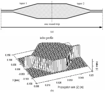
Figure 3.5 One round-trip of (a) the linear tapered waveguide structure and (b) the refractive-index profile applied in the BPM modelling. ... 66
Figure 3.6 Evolution of the intensity in the one round-trip through the tapered waveguide, with higher intensities denoted by whiter colours. ... 67
Figure 3.7 Fabrication procedure... 70
Figure 3.8 Cleaning procedure... 71
Figure 3.9 Top view of the experimental cavity set-up for the Ti:sapphire pumped channel and tapered waveguide lasers... 74
Figure 3.10 Absorbed pump power threshold against maximum taper width for the linear and parabolic tapered-waveguide lasers, alongside the standard channel waveguide lasers. ... 75
Figure 3.11 Slope efficiency against maximum taper width for the linear and parabolic tapered- waveguide lasers, alongside the standard channel waveguide lasers... 76
Figure 3.12 Imaged mode profiles for the 200µm-wide linear (upper) and parabolic (lower) tapers... 77
Figure 4.1 Typical pump configuration of a diode end-pumped waveguide laser: (a) coupling scheme for the diode “slow” axis, and (b) for the “fast” axis. ... 87
Figure 4.2 Schematic representation of diode to waveguide proximity coupling. ... 88
List of Figures
Figure 4.4 Cross-section comparison of a “classical” single-mode double-clad fiber and a large-mode-area double-clad planar waveguide. ... 89 Figure 4.5 Schematic structure of a double-clad planar waveguide. ... 91 Figure 4.6 One-dimensional step-function doping of a double-clad planar waveguide,
with the doping ratio tcore/tw... 95 Figure 4.7 Relative gain for the first four guided modes at 1064nm against doping
fraction for a resonating one-directional power 100 times greater than the saturation power. ... 96 Figure 4.8 Doping fraction at which the gain for mode 1 becomes equal to that for
mode 0, relative to value of I/Isat. ... 96 Figure 4.9 Extended stable cavity resonator design... 97 Figure 4.10 A computer modelling on the real lens extended cavity with two
cylindrical lenses, showing beam radii for the two axes with the change of the cavity length. ... 98 Figure 4.11 Pump set-up of a diode-bar side-pumped Nd:YAG double-clad planar
waveguide laser. ... 99 Figure 4.12 Output beam quality factor against relative position of the output coupler,
with T=19% and an optimum cavity length of ~120mm. The inset shows the optimized collimated output captured on a CCD camera... 100 Figure 4.13 Output power against absorbed pumped power for the high-brightness
and multimode cavities and an output coupling of Roc = 0.70. ... 101 Figure 5.1 A photo of a typical diode stack structure with the collimating
micro-lenses, downloaded from www.nuvonyx.com. ... 108 Figure 5.2 (a) Photo and (b) schematic for the collimated diode stack structure. .... 109 Figure 5.3 Procedure of the design of the diode-stack-to-waveguide coupling optics.
... 110 Figure 5.4 Two lens combination models on the y-axis of the diode and the beam size
List of Figures
side-pumped waveguide laser; (c) the double-clad waveguide structure with the dimensions; and finally (d) a photo of the set-up... 115 Figure 5.6 The 30μm Nd:YAG waveguide laser output power versus incident pump
power with single-side pumping from two diode stacks No.1 and No.2, respectively... 117 Figure 5.7 The 30μm Nd:YAG waveguide laser output power versus absorbed pump
power with double-side pumping from two diode stacks... 117 Figure 5.8 Some typical areas observed under microscope on (a) the
HR-mirror-attached end face, and (b) the 20%-output-coupler end face of the waveguide after the upper sapphire cladding layer dropped off from the rest of the waveguide... 119 Figure 5.9 Schematic of the extended cavity configuration combined with the stack
pumping... 121 Figure 5.10 Modelling of the spherical+cylindrical lens extended cavity, showing
beam radii for the two axes of the waveguide with the change of the cavity length. ... 122 Figure 5.11 The output power against absorbed pump power of the
diode-stack-pumped 30μm Nd:YAG Waveguide laser with a stable extended cavity. ... 123 Figure 5.12 Some typical areas on (a) the HR-mirror-attached end face, and (b) the
AR-coated end face of the waveguide after laser operation with an
extended cavity... 124 Figure 5.13 Design of the 50µm Yb:YAG planar waveguide structure. ... 125 Figure 5.14 Theoretical modelling on the laser performance of an 50µm Yb:YAG
planar waveguide laser pumped by two diode stacks with maximum
incident power of 360W. ... 126 Figure 6.1 Experimental set-up of the PLD chamber apparatus [1]. ... 132 Figure 6.2 Experimental arrangement for the pump configuration and laser output
analysis for the diode-stack end-pumped 50µm-thick Nd:GGG PLD
waveguide laser. ... 133 Figure 6.3 The 50μm Nd:GGG PLD waveguide laser output power versus absorbed
pump power by diode-stack end pumping with a Roc=0.8714 output
List of Figures
Figure 6.4 Output beam profile of the 50μm Nd:GGG PLD waveguide laser pumped by a three-bar diode stack... 136 Figure 6.5 Findlay-Clay plot according to the laser threshold measurements of the
50μm Nd:GGG PLD waveguide laser, to estimate the propagation losses. ... 137 Figure 6.6 Theoretical plot for the field amplitude contours of a self-imaging
multimode symmetric step-index Nd:GGG/YAG waveguide of depth 50µm, with an axially symmetric input beam. ... 139 Figure 6.7 Schematic of the experimental set-up of the self-imaging effect observing.
... 139 Figure 6.8 Beam profile of (a) multimode propagation through the Nd:GGG
List of Tables
List of Tables
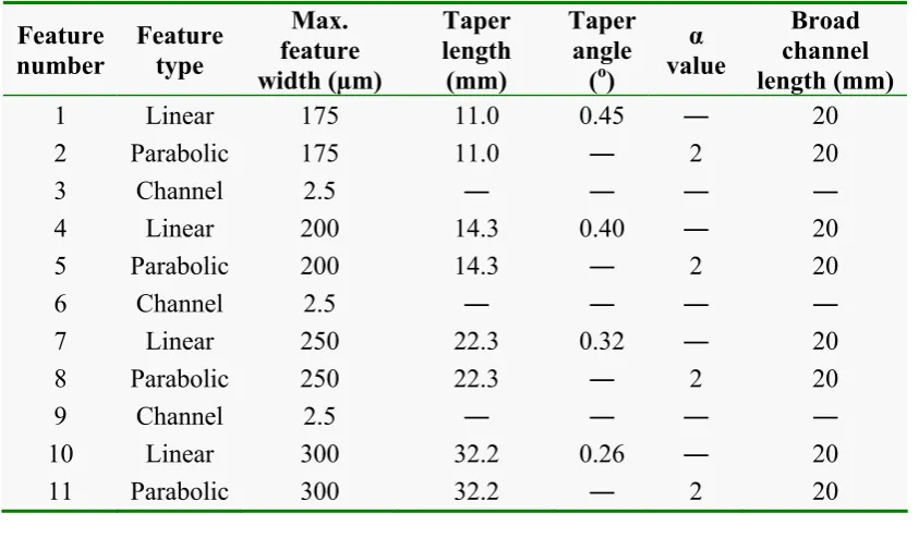
Table 3.1 Design features of the photolithographic mask: linear and parabolic tapers. ... 65 Table 3.2 Summary of laser performance for the three types of waveguides... 76 Table 3.3 Design features of sample LT and sample BC... 78 Table 3.4 Slope efficiency results and spatial overlap calculation of sample LT and
sample BC. ... 79 Table 5.1 A comparison of the experimental results and Zemax modeling on the
optimum lens combination for the diode-stack beam focusing, alongside the power delivery efficiency through a 50μm aperture and a 30μm
aperture, respectively... 113 Table 5.2 Yb:YAG laser model parameters... 125 Table 5.3 Thermal parameters used in the Yb:YAG waveguide model described.. 127 Table 6.1 Absorbed pump power threshold with different output coupler
transmissions. ... 135 Table 7.1 The key parameters applied in the experimental chapters (Chapter 3 – 6)
Author’s Declaration
Author’s Declaration
I, Jing Wang, declare that the thesis entitled High-Average-Power Planar Waveguide Lasers and the work presented in it are my own. I confirm that:
• this work was done wholly or mainly while in candidature for a research degree at the University of Southampton;
• where any part of this thesis has previously been submitted for a degree or any other qualification at this University or any other institution, this has been clearly stated;
• where I have consulted the published work of others, this is always clearly attributed;
• where I have quoted from the work of others, the source is always given. With the exception of such quotations, this thesis is entirely my own work;
• I have acknowledged all main sources of help;
• where the thesis is based on work done by myself jointly with others, I have made clear exactly what was done by others and what I have contributed myself;
Acknowledgements
Acknowledgements
Here it comes finally. I’ve been looking forward to writing this page for years by now, but when the day arrives, I start to realize the difficulty to squeeze everyone that has helped me into one page. Thus first I’d like to say: to each of you, I do feel very grateful.
I’d like to thank my supervisor Dave for being so helpful with my work, being patient with my stupidity, being understanding when I met difficulties during the thesis writing, and never been angry with me even when I broke the waveguide. Thanks to Dave for being a perfect supervisor in every student’s dream and choosing me in the first place!
I’d like to thank Jacob for being there helping me throughout the project and being able to give me a smile every time I walked into his office with emergency panic. Thanks also to Cheng and Simon for guiding me in the labs during my first year, which, believe me, is not the easiest job in the world. Thanks to Tim for providing his excellent waveguides and working with me in the labs. Thanks to all of the technicians for making things for me and teaching me “lab English” such like “screwdriver” and “allen key”, and in particular thanks to Simon who taught me how to use Autocad and Dave for helping me in the cleanroom. Thanks also go to everyone else at the ORC who helped to make my work possible.
I’d like to thank Yoong for being such a good friend and thank ORC for giving me the chance to know her. Thanks also to my office mates for giving me such a pleasant office to work in. Special thanks to Francesca for helping to print, bind and submit the thesis. Thanks to Lingqian for sending me all the food parcels from China. Thanks also go to Huizhi for all the international phone calls she made to me and listening to me no matter what.
Symbols and Abbreviations
Symbols and Abbreviations
1D One-dimensional 1
A - A5 Constants
AR Anti-reflection
ASE Amplified spontaneous emission
b and b′ Normalised mode effective indices
BPM, FD-BPM, and FFT-BPM
Beam propagation method, finite difference method, and fast Fourier transformation method
c Speed of light in vacuum
CW Continuous wave
1
d - d4 Depths
core
d Depth of the doped region
x
d and dy Decay of the index profile in the lateral and depth directions respectively
) , , (x y z
d Normalized doping profile in the laser medium
D Diameter
v
D and De “Variance” diameter and “ 2
1 e ” diameter DI Deionised
E Electric field
x
E , Ey, and Ez x, , and y z-components of the electric field respectively Y
E Young’s modulus
) , (x y
E x and dependence of the electric field function of a guided mode
y
f Sum of the occupation factors for the lower ( ) and upper ( ) laser Stark levels
1
f
2
Symbols and Abbreviations
l L
f Final laser Stark level Boltzmann occupation factor p
L
f Initial pump Stark level Boltzmann occupation factor l
U
f Initial laser Stark level Boltzmann occupation factor p
U
f Terminal pump Stark level Boltzmann occupation factor
s
F Safety factor (to express the fracture possibility of the host material)
A
F Fraction of pump power absorbed in a single pass through the
width of the laser medium
B
F Fraction of laser power “absorbed” in a single pass along the
length of the laser medium p
G Gain for the pth laser mode with spatial distribution φp rel
G Relative gain for the pth laser mode GGG Gadolinium gallium garnet (Gd3Ga5O12)
h Planck’s constant
H Magnetic field
x
H , Hy, and Hz x, , and y z-components of the magnetic field respectively )
, (x y
H x and dependence of the magnetic field function of a guided mode
y
HR High-reflection )
(x
I and I(y) Intensity distribution across the transverse co-ordinates x and respectively
y
0
k Wave vector in free space
y
k2 and k1y y-axis wave vector within the waveguide core in Chapter 2 and 4 respectively
s
k , ky, and kdy Thermal conductivity of the layers of sapphire, YAG, and doped-YAG respectively
z
k
ky
, k(y), and )
(y
z-axis wave vector, y dependence of the wave vector, and y dependence of the y-axis wave vector respectively
) , , (x y z
k Thermal conductivity
l Length of the laser medium
L Taper length, in Chapter 3
Round-trip loss exponent, in the rest of the thesis SI
L Self-image period length 2
M Beam propagation factor 2
Symbols and Abbreviations
2 y
M y-axis beam quality
MMI Multimode interference
MOPA Master oscillator - power amplifier
n Refractive index of the laser medium at the laser wavelength
0
n - n5 Refractive indices of different waveguide regions, as defined in respective chapters
0 1
n Total population in the lower laser level at thermal equilibrium
core
n and ncladding Refractive indices of the waveguide core and cladding layers respectively
eff
n′ Effective index of the fundamental mode in the channel waveguide with finite width W
eff
n Effective index of the fundamental mode within a planar waveguide of equal depth (W →∞)
A
n , nL, and nU
Active ions in all ( ) of the laser manifolds, the lower ( ) and upper ( ) manifold respectively, in terms of population density
A
n nL
U n
1
N and N2 Population density of the lower and upper laser levels
respectively 0
1
N Population density of the lower laser level at thermal equilibrium
L
N and NU Total population density of the lower and upper manifolds respectively
l U N
Integrated inversion density with respect to the laser crystal length and referenced to the Stark levels coupled by the laser radiation
p U N
Integrated inversion density with respect to the laser crystal width and referenced to the Stark levels coupled by the pump radiation
NA Numerical aperture
OC Output coupler
abs
P Absorbed power
cav
P Laser power in the cavity h
P Uniformly deposited heat in
P Incident power
l
P Laser power travelling in one direction inside the laser cavity p
Symbols and Abbreviations
PLD Pulsed laser deposition
PWL Planar waveguide laser )
(z
q Complex beam parameter (as a function of ) z
) , ,
(x y z
QT Thermal power loading per unit volume )
, , (x y z
rp Normalised pump energy distribution
R Total pump rate
ex de
R − De-excitation rate of the lasing ions for a double pass in the gain medium
ex
R Rate at which ions are excited into the upper laser manifold by the pumping process
oc
R Reflectivity of the output coupler at the laser wavelength s
R Thermal shock parameter sy
R and Rss Thermal shock parameters of YAG and sapphire respectively )
(z
R Radius of wavefront curvature (as a function of ) z
RE Rare earth
S Degree of saturation caused by the intra-cavity laser power
core
t Waveguide core thickness w
t Waveguide thickness
a
T Average temperature
1 htsk
T and Thtsk2 Fixed temperatures of the lower and upper heat sinks respectively
oc
T Transmission of the output coupler ow
T One-way cavity transmission )
, , (x y z
T Temperature distribution
TE Transverse electric
TIE Thermal ion exchange TIR Total internal reflection
TM Transverse magnetic
UV Ultraviolet
V and V′ Normalised guide widths
0
w and W0 Waist radii of the fundamental and higher-order-mode beams respectively
c
w Width of the laser medium crystal )
(z
Symbols and Abbreviations
0
W and Wmax Initial channel width and maximum taper width of the tapered waveguide
) (z Wl
) (z Wp
, and Widths of the linear and parabolic tapers respectively (as a function of ) z
x
W and Wy Beam sizes of higher-order modes in the x and directions respectively
y
YAG Yttrium aluminium garnet (Y3Al5O12)
α Structure expansion coefficient y
1
α - α5y Decay coefficients in regions 1 to 5 of the waveguide
p
α Absorption coefficient of the laser medium at the pump
wavelength L
α Propagation loss coefficient
T
α Thermal expansion coefficient
γ Additional round-trip loss as a result of the taper structure
δ Background propagation loss coefficient
n
Δ Refractive index difference 0
N
Δ Population-inversion density at thermal equilibrium )
, , (x y z N
Δ Population-inversion density
ε Electric permittivity 0
ε Electric permittivity in free space 1
ε - ε5 Electric permittivity of regions 1 to 5
a
η Absorption efficiency (fraction of incident pump power absorbed in the laser medium of length l with absorption
coefficient αp) del
η Pump delivery efficiency lo
η Laser overlap with the doped region of the laser medium
mode
η Fill factor of the laser beam with respect to the laser gain
cross-sectional area
pl
η Spatial overlap of the pump and laser beams inside the laser
medium po
η Pump overlap with the doped region of the laser medium slope
η Laser slope efficiency
L
η Launch efficiency
Symbols and Abbreviations
max
θ
p
θ Projection angle of the ray of the fundamental mode in the
waveguide plane t
θ Angle of the taper barrier with the -axis z
Θ Beam divergence angle of higher-order-mode beams
λ Wavelength
0
λ Free-space wavelength
1 htsk
λ and λhtsk2
Surface heat transfer coefficients of the lower and upper heat sinks respectively
l
λ and λp Wavelengths of the laser and pump radiation respectively
μ Magnetic permeability
0
μ Magnetic permeability in free space 1
μ - μ5 Magnetic permeability of regions 1 to 5
ν Poisson’s ratio
l
ν and νp Frequencies of the laser and pump radiation respectively
σ Gain cross section
l
σ Spectroscopic laser emission cross section p
σ Spectroscopic pump absorption cross section
s
σ and σmax Surface stress and stress fracture limit that can be tolerated by the laser host material prior to fracture
x
σ and σy “Variance” width across the transverse co-ordinates x and respectively
y
τ Lifetime of the upper laser-level manifold eff
τ Effective emission lifetime of the upper laser level )
,z y , ( 0 x
φ Normalised laser photon distribution p
φ Normalised spatial distribution of the pth laser mode
U
φ and φL
Phase delays for plane waves propagating through the upper and lower half of the waveguide
Φ
A
Total cavity photon number
χ and χB Effective boundaries
ψ and ψ′ Phase offset
ω Angular frequency
p
ω and ωl
Chapter 1 Introduction
Chapter 1
Introduction
1.1
High-power diode-pumped solid-state lasers
There has been a significant enhancement in the field of high-power solid-state lasers in recent years, largely due to the development of reliable and cheap laser diodes as pump sources with more and more choices of wavelengths and power since the late 1980s [1-3]. The result is compact, efficient and robust laser sources which are attractive in the scientific, industrial, medical and military fields. Solid-state lasers operating at high power from ~1W to ~2kW have been demonstrated with different pumping schemes (end pumping, side pumping, and face pumping), various formats (rods, slabs, thin disks, waveguides, and fibres) for different active media and cavity designs [4-16].
This thesis describes the progress leading to higher-average-power diode-pumped planar waveguide lasers, which take advantage of the slab-like geometry of the planar waveguides. To gain an insight into the motivations and directions of the research, it is useful to start with some key parameters for developing a high-average-power solid-state laser.
Chapter 1 Introduction
lamp pumps, diode lasers are attractive for many reasons, primarily based on increased system efficiency, narrower spectral emission, longer lifetime, reliability, and highly improved output beam quality [17]. Their efficiencies of more than 50% [18] make diode lasers ideal pump sources for solid-state lasers. Moreover, the pump wavelength is selective and can be tuned to precisely match the peak absorption of the active ions, thus reducing the heat load which results from the difference between the pump and laser wavelength and significantly increasing the solid-laser system efficiency and beam quality. Diode lifetime can be on the order of 104 hours in continuous wave (CW) operation [19], compared to less than 1000 hours for the lifetime of flash lamps, which enables a reliable laser system. One characteristic feature of diode lasers in contrast to lamps is that their radiation can be focused rather easily to spatially match the solid-state laser mode. Solid-state lasers may be in the form of various geometric configurations: a rigid cylindrical rod, a slab, or an optical fibre, while diode lasers can lend themselves very well as pump sources in all these cases. The good overlap between the pump radiation and the laser mode volume again leads to the high overall system efficiency.
Compared to diode-pumped solid-state lasers, the direct use of diodes gives output with broader linewidth, lower peak powers, and lower brightness, limiting many applications, although it should be noted that they can be directly used in applications such as surface hardening or soldering which need only a moderate power density, about 104 W/cm2, within a relatively broad focal area [20].
Chapter 1 Introduction
4 4 4 4
2
1.1.2
Active ion and host material
With the pump source available, a proper active medium must be chosen, which should provide sharp fluorescent lines, strong absorption, and reasonably high quantum efficiency along with good optical and thermo-mechanical properties.
As mentioned in the last section, the emission wavelengths of diode lasers can be adjusted to match the peak absorption of important solid-state laser ions including, for instance, Nd3+ [23, 24], Er3+ [25, 26], Tm3+ [27, 28], Cr3+ [29, 30] and Yb3+ [31-33], depending on what laser wavelength is required. Rare earth (RE) ions are used in solid-state lasers as the active ions because of their sharp fluorescent transitions covering much of the near-infrared portions of the electromagnetic spectrum [34], trivalent ions being the most commonly used. The characteristic feature of RE3+ ions is that their fluorescence spectra arise from electronic transitions between levels of the partially filled 4f electron subshell, which is well shielded by the filled 5s and 5p outer shells. Electrons present in the 4f shell can be raised by the light absorption into unoccupied 4f levels.
Nd3+ is an excellent dopant for diode-pumped solid-state lasers and remains one of the most important elements among trivalent rare earth ions. The principle host materials are yttrium aluminium garnet Y3Al5O12 (YAG) and glass, where stimulated emission is gained at a number of frequencies within four spectral regions centred at 0.94, 1.06, 1.35, and 1.83μm [34], due to the 4 , , transitions, respectively. The 4-level transition 4 is the one that will be discussed in later chapters, and is shown in Fig. 1.1.
, 2 / 9 2 /
3 I
F →
2 / 11 4 2 /
3 I
F →
2 / 11
I I13/2 I15/2
The Yb3+ ion has a very simple energy level diagram (see Fig. 1.2) that consists of the ground state and 2 excited state manifolds separated by about 10,000 cm-1. The pumping scheme shown in Fig. 1.2 leads to a smaller quantum defect (see section 1.1.4), and consequently lower thermal loading [35-37], as compared to the Nd:YAG laser system discussed above, which makes the Yb3+ ion a promising alternative to the
2 / 7
Chapter 1 Introduction
more interest [39] for high-power systems, especially where thermal limitations can be the main consideration.
11509 cm-1
[image:27.595.138.502.140.378.2]Figure 1.1 Energy level diagram of Nd:YAG lasing at 1064nm.
Figure 1.2 Energy level diagram of Yb:YAG laser system.
Other advantages of Yb:YAG are the broad absorption bandwidth (18nm) [40] at the InGaAs wavelength, which is about 10 times broader than the 808nm absorption in Nd:YAG, and that Yb:YAG has a long lifetime of 951µs [34] - about 4 times longer
4
10929 10679 10624 10327
785 612 565 0 cm-1 2
F5/2
2
F7/2
1030nm pump
lasing 941nm
4F
3/2
4
I15/2
4
I13/2
4
I9/2 4
I11/2
4F
5/2 4F3/2
1064nm
4I
15/2
4
I13/2
4I
9/2 4
I11/2
11425
857 317 195 131 0 cm-1 2114 cm-1 ~4000 cm-1 ~6000 cm-1
808nm lasing
pump
laser transition
Chapter 1 Introduction
that, being a quasi-three-level laser Yb:YAG has higher laser threshold and has to be pumped much higher than threshold to gain an efficient operation.
Solid-state host materials can largely be grouped into crystalline solids and various glasses. To select a host material for a laser ion, optical properties would be the first considerations, avoiding poor beam quality after the beam propagation through the crystal. Most high-average-power laser systems need to take thermal effects into account, so that crystalline materials with high thermal conductance qualities will be a good choice. YAG is a very hard, isotropic crystal and has a good thermal conductivity (with a “thermal shock parameter” R=7.9W/cm [41], for example) and has consequently achieved a position of dominance among solid-state laser host materials.
In this work we will use YAG, glass, and gadolinium gallium garnet Gd3Ga5O12 (GGG) as host materials, with YAG and GGG used for high-power diode pumping and glass for its cheapness and compatibility with integrated optics.
1.1.3
Thermal considerations
Thermal problems and heat removal are usually a critical issue for designing high-average-power laser systems.
Chapter 1 Introduction
power is about 0.3 [43, 44] under conditions of laser extraction for a diode-pumped Nd:YAG laser pumped at 808 nm.
Heat generation takes place in the volume of the gain medium, while surface cooling required for heat extraction functions at the edges, either by a flow of coolant or by the conduction to a heat sink. Therefore, a non-uniform temperature distribution and consequently mechanical stress will occur with the combination of the “hot” laser medium and surrounding cooling devices, which results in a temperature- and stress-dependent variation of the refraction index [41]. Due to this index gradient, the laser beam will be distorted in the laser material, leading to various thermal effects, such as thermal lensing [45-47], stress-induced birefringence [48], and greatly increased surface stress or even fracture [49, 50], etc. These thermally induced problems severely degrade the beam quality and eventually limit the laser output power [51], which makes thermal management an essential part of high-average-power solid-state laser design.
To effectively remove heat from the gain material, sufficient cooling should be applied to the laser system. With reference to cooling techniques, the primary methods include liquid cooling (of which water-cooling is the most commonly used), air or gas cooling, and conductive cooling, which are associated with different host medium geometries. The four basic host medium geometries are the rod, fibre, slab, and thin-disc, the heat removal schematic of which are shown in Fig. 1.3.
Chapter 1 Introduction
Figure 1.3 Schematic of the heat removal of the four basic host medium geometries: (a) rod, (b) fibre, (c) thin-disk, and (d) slab.
Fibre lasers offer the possibility to overcome the thermal limitations for high-power lasers and to maintain the beam quality. The thermal load caused by the pumping process is spread over a very long region and heat is more efficiently removed, and thus the observed temperature increase in the laser core is small [58] compared to conventional rod lasers. Moreover, the refractive index profile of the fibre is dominantly defined by the geometrical dimensions and the numerical aperture of the waveguide structure itself, so that fibre lasers are nearly immune to the index-related thermal-optical effects. However, coupling optics needs to be chosen carefully, to ensure efficient diode-to-fibre coupling, especially with low-brightness high-power laser diodes.
On the other hand, the basic concept of the thin-disk laser [57] is to use a very thin active medium (thickness about 200µm) with one face mounted closely onto a heat sink. The thin-disk design reduces the pump-volume-to-cooling-surface ratio of the crystal drastically, so that high pump densities can be applied without a high-temperature rise within the crystal. Moreover, the one-dimensional heat flux, which is collinear with the lasing axis, strongly reduces the thermal distortions compared to the
to make the laser medium very short
to make the laser medium long and thin (a)
(b)
(c) (d)
Chapter 1 Introduction
imaged onto the disk under oblique angles (to separate it from the laser beam) and needs to multi-pass the disk to exploit the non-absorbed fraction.
The slab lasers take advantage of both the high cooling-surface-to-pump-volume ratio and the one-dimensional temperature gradients in the laser medium. It has been shown that the slab geometry promises a better thermal handling capability [49] compared to the cylindrical rod geometry. The slab structure suggests three possible pump schemes that will be discussed in section 1.2.3, and lends itself well to various solid-state laser systems with different requirements. When it comes to quasi-three-level media, a side pump scheme allows a longer absorption path than the thin disk and hence a lower doping level, which allows greater power scalability [59]. In this work, the planar waveguide, as stated in the next section, has the geometry of an extreme slab and shares the excellent thermal qualities discussed above.
1.2
High-power planar waveguide lasers
Fig. 1.4 shows a typical planar waveguide that might be used for high-power laser operation. The pump and laser light are confined in the RE-doped core, which has higher refractive index than the surrounding substrate and cladding regions.
Figure 1.4 A typical planar waveguide structure and guiding condition.
This thesis describes significant progress towards high-average-power diode-pumped planar waveguide lasers.
cladding n=n1
substrate n=n3 2
n n
core =
Guiding condition
Chapter 1 Introduction
1.2.1
Motivations
Planar waveguide laser (PWL) devices are of interest for many reasons. For example, planar optical waveguides are the key platform on which to construct integrated optical circuits, with multiple functions such as optical couplers, switches, interferometers, modulators, amplifiers and detectors, etc. Moreover, in recent years [13, 60-63], planar waveguides have been shown to be attractive in high-average-power diode-pumped lasers.
Compared to their bulk counterparts, the optical confinement offered by planar waveguides leads to lowering of the laser threshold pump power, if the waveguide propagation loss is also low, making operation well above lasing threshold achievable for moderate pump powers. The confinement also effectively stops free-space divergence and results in a high pump intensity and therefore a high gain per unit pump power. In addition, the optical guidance dominates the thermal lensing effect in the guided axis, and so the output laser beam quality in this axis is defined by the waveguide structure itself. Furthermore, planar waveguide lasers are very compact, making them convenient for use in many applications where large bulk lasers are not feasible.
As a format of the laser active medium, planar waveguides benefit from their extreme slab geometry. In comparison to bulk and fibre lasers, planar waveguide lasers offer a rectangular pump aperture which is perfectly fitted to the diode-bar geometry, allowing simple coupling optics or even proximity coupling [64] without beam shaping. There is also a greater degree of versatility concerning the pump arrangement, with three possible geometries possible (end-pumping, side-pumping, and face-pumping, see section 1.2.3). With side-pumping, in particular, the slab structure allows unique axes of operation on pumping, lasing and cooling, which leads to a simpler laser system design than thin-disk lasers.
Chapter 1 Introduction
NA
waveguide, and the stress fracture limit can be pushed to extreme values [65]. As opposed to the two-dimensional heat flow in bulk and fibre lasers, planar waveguide lasers create one-dimensional heat flow and therefore one-dimensional thermal gradient, which provides well defined birefringence axes avoiding depolarization loss.
It should also be noted that, compared to fibres, planar waveguides can involve almost any type of optical material, whereas fibre materials are mainly limited to types of glass due to fabrication limitations.
1.2.2
Waveguide fabrication
Waveguide fabrication procedures can be broadly grouped into two types: modification of the material refractive index and conjunction of materials with dissimilar refractive indices. The former can be subdivided into techniques such as ion-exchange [66], ion-diffusion [67], ion-implantation [68], and optical writing [69]. As an alternative, waveguides can also be fabricated by the techniques of deposition [70], epitaxial growth [71], and bonding [72]. These latter techniques generally have a stronger capability to produce high numerical aperture ( ) waveguides, which can be preferable for more efficient diode pumping [73], while the former techniques are generally preferred for integrated optical circuits.
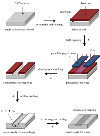
Ion exchange has been used to produce a refractive index difference in glass to make waveguides since 1972 [74]. The sample substrate is immersed in a bath of molten salts, so that the alkali ions in the salt bath slowly exchange with the ions in the substrate, leading to a small refractive-index change. The rate of the ion-exchange process can be controlled by the diffusion temperature and the assistance of an electric field across the substrate. Different waveguide patterns (channels, tapers, etc.) can be achieved by using relevant masks, which will be applied to the tapered- waveguide fabrication for diode-stripe-pumped integrated-optics compatible 1W-class waveguide lasers, as discussed in Chapter 3.
To achieve sufficient NA to allow high-power diode bar and diode-stack pumping,
Chapter 1 Introduction
NA
surfaces of two pieces of different bulk materials are polished to an optical flatness and free of any dirt or other particles, because they are expected to bond together without the use of any adhesive by Van der Waal’s intermolecular forces. To access Van der Waal’s forces, the two surfaces have to be brought together within molecular interaction distances, so that high-quality polishing is required to achieve surface flatness figures on the tens to hundreds of nanometre scale. In the case of thermal bonding [76], the process is assisted by a heat treatment. The use of these waveguides for high-power diode bar and diode-stack pumping will be discussed in Chapter 4 and 5, respectively.
Thin film waveguides, fabricated by pulsed laser deposition (PLD) [77], also have the potential for producing garnet waveguides of sufficient to allow high-power diode pumping. A pulsed laser (usually at ultra-violet wavelength) is used to ablate a target, and the ejected material forms a plasma plume, which then expands away from the target surface and interacts with the chamber atmosphere until it reaches the substrate where it is deposited as a thin film. In this technique, the substrate can be heated to assist with nucleation and allow crystal growth, and a background gas can be used to help control the film composition. Such waveguides are assessed for their potential for output power scaling with diode-stack pumping in Chapter 6.
1.2.3
Pump scheme
Efficient pump schemes are needed to couple the radiation from a diode laser to the planar waveguide. Three possible pump configurations (face-pumping, side-pumping and end-pumping) are shown in Fig. 1.5, appropriate for the slab/waveguide geometry. These configurations in turn have different requirements on the schemes of diode to crystal coupling: to give focussing in both axes in the case of end-pumping, single axis focussing for side-pumping, and to provide sufficient absorption in face-pumping configurations.
Chapter 1 Introduction
lasing
pumping requires multipass pump optics to be used, such as a reflective, slotted mirror pump chamber [78] to increase the absorption efficiency, which adds to the complexity of the laser system.
a. face pumping pumping
waveguide
lasing
b. side pumping
pumping waveguide
lasing
c. end pumping pumping
[image:35.595.159.483.154.718.2]Chapter 1 Introduction
In a side-pumped laser system (Fig. 1.5.b), the pump beam is incident on the edge of the waveguide perpendicular to the laser beam. Side pumping is favoured in some cases, especially in high-average-power systems, where it is rather difficult to deliver an adequate amount of pump power through the small end faces of the laser crystal. A significant advantage of the side-pumped geometry is that power scaling can be simply achieved by increasing the length over which the waveguide is pumped to allow in more pump power, or by pumping from both sides. Furthermore, side pumping uses separate crystal surfaces for pumping, cooling, and laser extraction for individual optimisation, which significantly simplifies the laser system design. The design modelling in ref. [59] shows that edge pumping of quasi-three-level systems is in theory superior to face pumping due to more flexibility in choosing doping level.
End pumping (Fig. 1.5.c) causes the pump radiation to be absorbed along the longitudinal axis of the laser medium, which results in near total absorption of the pump and, therefore, in high laser efficiency. It also has the advantage that good overlap is obtained between the pump volume and the laser mode, leading to improved mode control and beam quality [79], but is limited in terms of power scalability [80] compared to the face and side pumping configurations.
1.2.4
Historical review
The first lasing waveguide structures date back to the 1960’s, when fibres were employed to reduce the threshold in laser systems [81], and in 1971 the first operation of a planar waveguide laser was reported [82]. Since then, a large range of techniques has been applied to the fabrication of waveguides and a host of materials have been studied as the potential active media [71, 83-85].
The contributions to the development of high-average-power diode-pumped waveguide laser systems can be largely divided into two groups by the different schemes of pumping arrangements, in-plane pumping (end and side pumping) and face pumping.
Chapter 1 Introduction
2
by the first diode-pumped Yb:YAG planar waveguide laser in 1995 [87]. In 1997, with the thermal-bonding technique [72], planar waveguides were fabricated with high numerical aperture, low propagation loss, and good thermal properties that are necessary for high-power diode-bar pumping. A lot of improvements were presented in the following two years in obtaining more average output power and (nearly) diffraction-limited beam quality. In 1998, Bonner et al. [88] reported a 6.2W CW PWL from an 80µm-thick multimode Nd:YAG waveguide that was grown via liquid phase epitaxy. The following year [73] a much smaller 8µm-thick Nd:YAG waveguide produced 3.7W output power, fabricated with direct bonding. With the same technique, laser performance of a 100µm-thick 10at.% multimode Yb:YAG waveguide was reported by Griebner et al. [76]: a maximum CW output power of 1.2W was obtained and near-diffraction-limited output ( M values 1.5x4) was achieved by using an astigmatic resonator. Based on the technique of direct bonding, proximity coupling and double-clad structures were developed and reported by Bonner et al. [64]. It should be mentioned here that in this paper the authors described the technique of proximity coupling the diode-bar radiation to the planar waveguide without coupling optics, which probably led to the simplest pump scheme so far and provided efficient diode pumping, practically demonstrated in [89] by Beach et al. with >12W obtained from a side-pumped proximity-coupled double-clad Yb:YAG waveguide laser. In the same year, 15W output power [13] was achieved by side pumping again, from a double-clad Tm:YAG waveguide lasing at 2.02µm.
Chapter 1 Introduction
arrangement so far is 150W in multi-mode operation and >100W in a high-brightness configuration using an external unstable resonator [91].
1.3
Structure of this thesis
Chapter 1 Introduction
1.4
References
[1] T. Y. Fan and R. L. Byer, "Diode laser-pumped solid-state lasers," IEEE Journal of Quantum Electronics, vol. 24, pp. 895-912, Jun 1988.
[2] D. C. Brown, "Ultrahigh-average-power diode-pumped Nd:YAG and Yb:YAG lasers," IEEE Journal of Quantum Electronics, vol. 33, pp. 861-873, May 1997.
[3] N. V. Kravtsov, "Basic trends in the development of diode-pumped solid-state lasers," Quantum Electronics, vol. 31, pp. 661-677, Aug 2001.
[4] G. Cerullo, S. Desilvestri, and V. Magni, "High-efficiency, 40-W CW Nd:YLF laser with large TEM00 mode," Optics Communications, vol. 93, pp. 77-81, Sep 1992.
[5] S. C. Tidwell, J. F. Seamans, and M. S. Bowers, "Highly efficient 60-W TEM00 CW diode-end-pumped Nd:YAG laser," Optics Letters, vol. 18, pp. 116-118, Jan 15 1993.
[6] D. Golla, S. Knoke, W. Schone, G. Ernst, M. Rode, A. Tunnermann, and H. Welling, "300-W CW diode-laser side-pumped Nd:YAG rod laser," Optics Letters, vol. 20, pp. 1148-1150, May 15 1995.
[7] D. Golla, M. Rode, S. Knoke, W. Schone, and A. Tunnermann, "62-W CW TEM00 Nd:YAG laser side-pumped by fibre-coupled diode lasers," Optics Letters, vol. 21, pp. 210-212, Feb 1996.
[8] S. Konno, S. Fujikawa, and K. Yasui, "80 W CW TEM00 1064 nm beam generation by use of a laser-diode-side-pumped Nd:YAG rod laser," Applied Physics Letters, vol. 70, pp. 2650-2651, May 1997.
[9] V. Dominic, S. MacCormack, R. Waarts, S. Sanders, S. Bicknese, R. Dohle, E. Wolak, P. S. Yeh, and E. Zucker, "110W fibre laser," Electronics Letters, vol. 35, pp. 1158-1160, Jul 1999.
[10] Y. Hirano, Y. Koyata, S. Yamamoto, K. Kasahara, and T. Tajime, "208-W TEM00 operation of a diode-pumped Nd : YAG rod laser," Optics Letters, vol. 24, pp. 679-681, May 15 1999.
[11] C. Stewen, K. Contag, M. Larionov, A. Giesen, and H. Hugel, "A 1-kW CW thin disc laser," IEEE Journal of Selected Topics in Quantum Electronics, vol. 6, pp. 650-657, Jul-Aug 2000.
Chapter 1 Introduction
[13] J. I. Mackenzie, S. C. Mitchell, R. J. Beach, H. E. Meissner, and D. P. Shepherd, "15W diode-side-pumped Tm:YAG waveguide laser at 2 μm," Electronics Letters, vol. 37, pp. 898-899, Jul 5 2001.
[14] Y. Jeong, J. K. Sahu, D. N. Payne, and J. Nilsson, "Ytterbium-doped large-core fiber laser with 1.36 kW continuous-wave output power," Optics Express, vol. 12, pp. 6088-6092, Dec 13 2004.
[15] D. Gapontsev, "Quasi-single-mode fiber laser nears 2-kW output with high-quality beam," Laser Focus World, vol. 41, p. 9, Jun 2005.
[16] D. Y. Shen, J. K. Sahu, and W. A. Clarkson, "Highly efficient in-band pumped Er : YAG laser with 60 W of output at 1645 nm," Optics Letters, vol. 31, pp. 754-756, Mar 15 2006.
[17] D. W. Hughes and J. R. M. Barr, "Laser diode pumped solid state lasers," Journal Of Physics D-Applied Physics, vol. 25, pp. 563-586, Apr 14 1992.
[18] A. Tunnermann, H. Zellmer, W. Schone, A. Giesen, and K. Contag, "New concepts for diode-pumped solid-state lasers," in High-Power Diode Lasers: Fundamentals, Technology, Applications. vol. 78, R. Diehl, Ed.: Springer-Verlag Berlin Heidelberg, 2000, pp. 369-408.
[19] L. Marshall, "Laser Diode-Pumped Solid-State Lasers," in CLEO/QELS Baltimore, USA, 2005, p. SC165.
[20] U. Brauch, P. Loosen, and H. Opower, "High-power diode lasers for direct applications," in High-Power Diode Lasers: Fundamentals, Technology, Applications. vol. 78, R. Diehl, Ed.: Springer-Verlag Berlin Heidelberg, 2000, pp. 303-368.
[21] W. Koechner, Solid-state laser engineering - Chapter 6, 5th ed. vol. 1: Springer-Verlag Berlin Heidelberg New York, 1999.
[22] W. F. Krupke, "Ytterbium solid-state lasers - The first decade," IEEE Journal of Selected Topics in Quantum Electronics, vol. 6, pp. 1287-1296, Nov-Dec 2000.
[23] N. P. Barnes, D. J. Gettemy, L. Esterowitz, and R. E. Allen, "Comparison of Nd 1.06 and 1.33 μm operation in various hosts," IEEE Journal of Quantum Electronics, vol. 23, pp. 1434-1451, Sep 1987.
[24] T. Y. Fan and R. L. Byer, "Continuous-wave operation of a room-temperature, diode-laser-pumped, 946-nm Nd:YAG laser," Optics Letters, vol. 12, pp. 809-811, Oct 1987.
Chapter 1 Introduction
[26] D. W. Chen, C. L. Fincher, T. S. Rose, F. L. Vernon, and R. A. Fields, "Diode-pumped 1-W continuous-wave Er:YAG 3 μm laser," Optics Letters, vol. 24, pp. 385-387, Mar 15 1999.
[27] L. Esterowitz, "Diode-pumped holmium, thulium, and erbium lasers between 2 and 3 μm operating CW at room temperature," Optical Engineering, vol. 29, pp. 676-680, Jun 1990.
[28] C. Li, J. Song, D. Y. Shen, N. S. Kim, K. Ueda, Y. J. Huo, S. F. He, and Y. H. Cao, "Diode-pumped high-efficiency Tm : YAG lasers," Optics Express, vol. 4, pp. 12-18, Jan 4 1999.
[29] P. M. W. French, R. Mellish, J. R. Taylor, P. J. Delfyett, and L. T. Florez, "All-solid-state diode-pumped modelocked Cr-LiSAF laser," Electronics Letters, vol. 29, pp. 1262-1263, Jul 8 1993.
[30] D. Kopf, K. J. Weingarten, G. Zhang, M. Moser, M. A. Emanuel, R. J. Beach, J. A. Skidmore, and U. Keller, "High-average-power diode-pumped femtosecond Cr:LiSAF lasers," Applied Physics B-Lasers And Optics, vol. 65, pp. 235-243, Aug 1997.
[31] H. W. Bruesselbach, D. S. Sumida, R. A. Reeder, and R. W. Byren, "Low-heat high-power scaling using InGaAs-diode-pumped Yb:YAG lasers," IEEE Journal of Selected Topics in Quantum Electronics, vol. 3, pp. 105-116, Feb 1997.
[32] T. Dascalu, N. Pavel, and T. Taira, "90 W continuous-wave diode edge-pumped microchip composite Yb : Y3Al5O12 laser," Applied Physics Letters, vol. 83, pp. 4086-4088, Nov 17 2003.
[33] E. C. Honea, R. J. Beach, S. C. Mitchell, and P. V. Avizonis, "183-W, M2 = 2.4 Yb : YAG Q-switched laser," Optics Letters, vol. 24, pp. 154-156, Feb 1 1999.
[34] W. Koechner, Solid-state laser engineering - Chapter 2, 5th ed. vol. 1: Springer-Verlag Berlin Heidelberg New York, 1999.
[35] P. Lacovara, H. K. Choi, C. A. Wang, R. L. Aggarwal, and T. Y. Fan, "Room temperature diode-pumped Yb:YAG laser," Optics Letters, vol. 16, pp. 1089-1091, Jul 15 1991.
[36] T. Y. Fan, "Optimizing the efficiency and stored energy in quasi-three-level lasers," IEEE Journal of Quantum Electronics, vol. 28, pp. 2692-2697, Dec 1992.
Chapter 1 Introduction
crystals for laser applications," IEEE Journal of Quantum Electronics, vol. 29, pp. 1179-1191, Apr 1993.
[39] W. F. Krupke and L. L. Chase, "Ground-state depleted solid-state lasers - principles, characteristics and scaling," Optical And Quantum Electronics, vol. 22, Supplement 1, pp. S1-S22, Jul 1990.
[40] D. S. Sumida and T. Y. Fan, "Room-temperature 50-mJ/pulse side-diode-pumped Yb:YAG laser," Optics Letters, vol. 20, pp. 2384-2386, Dec 1 1995. [41] W. Koechner, Solid-state laser engineering - Chapter 7, 5th ed. vol. 1:
Springer-Verlag Berlin Heidelberg New York, 1999.
[42] U. Brauch and M. Schubert, "Comparison of lamp and diode pumped CW Nd:YAG slab lasers," Optics Communications, vol. 117, pp. 116-122, May 15 1995.
[43] T. Y. Fan, "Heat-generation in Nd-YAG and Yb-YAG," IEEE Journal Of Quantum Electronics, vol. 29, pp. 1457-1459, Jun 1993.
[44] B. Comaskey, B. D. Moran, G. F. Albrecht, and R. J. Beach, "Characterization of the heat loading of Nd-doped YAG, YOS, YLF, and GGG excited at diode pumping wavelengths," IEEE Journal Of Quantum Electronics, vol. 31, pp. 1261-1264, Jul 1995.
[45] W. A. Clarkson, "Thermal effects and their mitigation in end-pumped solid-state lasers," Journal of Physics D-Applied Physics, vol. 34, pp. 2381-2395, Aug 21 2001.
[46] S. Chenais, F. Balembois, F. Druon, G. Lucas-Leclin, and P. Georges, "Thermal lensing in diode-pumped ytterbium lasers - Part I: Theoretical analysis and wavefront measurements," IEEE Journal Of Quantum Electronics, vol. 40, pp. 1217-1234, Sep 2004.
[47] S. Chenais, F. Balembois, F. Druon, G. Lucas-Leclin, and P. Georges, "Thermal lensing in diode-pumped ytterbium lasers - Part II: Evaluation of quantum efficiencies and thermo-optic coefficients," IEEE Journal Of Quantum Electronics, vol. 40, pp. 1235-1243, Sep 2004.
[48] J. D. Foster and L. M. Osterink, "Thermal effects in a Nd:YAG Laser," Journal Of Applied Physics, vol. 41, pp. 3656-3663, 1970.
[49] J. M. Eggleston, T. J. Kane, K. Kuhn, J. Unternahrer, and R. L. Byer, "The slab geometry laser---part 1: Theory," IEEE Journal of Quantum Electronics, vol. 20, pp. 289-301, 1984.
Chapter 1 Introduction
[51] Y. F. Chen, C. F. Kao, T. M. Huang, C. L. Wang, and S. C. Wang, "Influence of thermal effect on output power optimization in fiber-coupled laser-diode end-pumped lasers," IEEE Journal of Selected Topics in Quantum Electronics, vol. 3, pp. 29-34, Feb 1997.
[52] R. Paschotta, J. Aus der Au, and U. Keller, "Thermal effects in high-power end-pumped lasers with elliptical-mode geometry," IEEE Journal Of Selected Topics In Quantum Electronics, vol. 6, pp. 636-642, Jul-Aug 2000.
[53] M. Tsunekane, N. Taguchi, T. Kasamatsu, and H. Inaba, "Analytical and experimental studies on the characteristics of composite solid-state laser rods in diode-end-pumped geometry," IEEE Journal Of Selected Topics In Quantum Electronics, vol. 3, pp. 9-18, Feb 1997.
[54] R. Weber, B. Neuenschwander, M. Mac Donald, M. B. Roos, and H. P. Weber, "Cooling schemes for longitudinally diode laser-pumped Nd : YAG rods," IEEE Journal Of Quantum Electronics, vol. 34, pp. 1046-1053, Jun 1998.
[55] W. C. Scott and M. D. Wit, "Birefringence compensation and TEM00 mode enhancement in a Nd:YAG Laser," Applied Physics Letters, vol. 18, pp. 3-4, Jan 1 1971.
[56] M. K. Davis, M. J. F. Digonnet, and R. H. Pantell, "Thermal effects in doped fibres," Journal of Lightwave Technology, vol. 16, pp. 1013-1023, Jun 1998. [57] A. Giesen, H. Hugel, A. Voss, K. Wittig, U. Brauch, and H. Opower, "Scalable
concept for diode-pumped high-power solid-state lasers," Applied Physics B-Lasers And Optics, vol. 58, pp. 365-372, May 1994.
[58] L. Zenteno, "High-power double-clad fiber lasers," Journal Of Lightwave Technology, vol. 11, pp. 1435-1446, Sep 1993.
[59] T. S. Rutherford, W. M. Tulloch, E. K. Gustafson, and R. L. Byer, "Edge-pumped quasi-three-level slab lasers: Design and power scaling," IEEE Journal of Quantum Electronics, vol. 36, pp. 205-219, Feb 2000.
[60] H. J. Baker, A. A. Chesworth, D. P. Millas, and D. R. Hall, "A planar waveguide Nd:YAG laser with a hybrid waveguide - unstable resonator," Optics Communications, vol. 191, pp. 125-131, May 1 2001.
[61] J. R. Lee, H. J. Baker, G. J. Friel, G. J. Hilton, and D. R. Hall, "High-average-power Nd:YAG planar waveguide laser that is face pumped by 10 laser diode bars," Optics Letters, vol. 27, pp. 524-526, Apr 1 2002.
Chapter 1 Introduction
[63] J. Q. Xu, "Quasi-self-imaging planar waveguide lasers with high-power single-mode output," Optics Communications, vol. 259, pp. 251-255, Mar 1 2006. [64] C. L. Bonner, T. Bhutta, D. P. Shepherd, and A. C. Tropper, "Double-clad
structures and proximity coupling for diode-bar-pumped planar waveguide lasers," IEEE Journal of Quantum Electronics, vol. 36, pp. 236-242, Feb 2000. [65] D. P. Shepherd, S. J. Hettrick, C. Li, J. I. Mackenzie, R. J. Beach, S. C.
Mitchell, and H. E. Meissner, "High-power planar dielectric waveguide lasers," Journal of Physics D-Applied Physics, vol. 34, pp. 2420-2432, Aug 21 2001.
[66] T. Findakly, "Glass waveguides by ion-exchange: A review," Optical Engineering, vol. 24, pp. 244-250, 1985.
[67] R. V. Schmidt and I. P. Kaminow, "Metal-diffused optical waveguides in LiNbO3," Applied Physics Letters, vol. 25, pp. 458-460, 1974.
[68] P. J. Chandler, L. Zhang, and P. D. Townsend, "Ion-implanted wave-guides in laser host materials," Nuclear Instruments & Methods - Physics Research Section B - Beam Interactions with Materials and Atoms, vol. 59, pp. 1223-1227, Jul 1991.
[69] M. Svalgaard, C. V. Poulsen, A. Bjarklev, and O. Poulsen, "Direct UV writing of buried singlemode channel waveguides in Ge-doped silica films," Electronics Letters, vol. 30, pp. 1401-1403, 1994.
[70] M. Kawachi, "Silica waveguides on silicon and their application to integrated-optic components," Optical and Quantum Electronics, vol. 22, pp. 391-416, 1990.
[71] I. Chartier, B. Ferrand, D. Pelenc, S. J. Field, D. C. Hanna, A. C. Large, D. P. Shepherd, and A. C. Tropper, "Growth and low-threshold laser oscillation of an epitaxially grown Nd:YAG waveguide," Optics Letters, vol. 17, pp. 810-812, Jun 1 1992.
[72] C. T. A. Brown, C. L. Bonner, T. J. Warburton, D. P. Shepherd, A. C. Tropper, D. C. Hanna, and H. E. Meissner, "Thermally bonded planar waveguide lasers," Applied Physics Letters, vol. 71, pp. 1139-1141, Sep 1 1997.
[73] D. P. Shepherd, C. L. Bonner, C. T. A. Brown, W. A. Clarkson, A. C. Tropper, D. C. Hanna, and H. E. Meissner, "High-numerical-aperture, contact-bonded, planar waveguides for diode-bar-pumped lasers," Optics Communications, vol. 160, pp. 47-50, Feb 1 1999.
Chapter 1 Introduction
[75] J. Haisma, B. Spierings, U. K. P. Biermann, and A. A. Vangorkum, "Diversity and feasibility of direct bonding - a survey of a dedicated optical-technology," Applied Optics, vol. 33, pp. 1154-1169, March 1 1994.
[76] U. Griebner, R. Grunwald, and H. Schonnagel, "Thermally bonded Yb : YAG planar waveguide laser," Optics Communications, vol. 164, pp. 185-190, Jun 15 1999.
[77] C. Grivas, T. C. May-Smith, D. P. Shepherd, and R. W. Eason, "Laser operation of a low loss (0.1 dB/cm) Nd : Gd3Ga5O12 thick (40 μm) planar waveguide grown by pulsed laser deposition," Optics Communications, vol. 229, pp. 355-361, Jan 2 2004.
[78] A. Faulstich, H. J. Baker, and D. R. Hall, "Face pumping of thin, solid-state slab lasers with laser diodes," Optics Letters, vol. 21, pp. 594-596, Apr 15 1996.
[79] L. R. Marshall, A. Kaz, and R. L. Burnham, "Highly efficient TEM00 operation of transversely diode-pumped Nd-YAG lasers," Optics Letters, vol. 17, pp. 186-188, Feb 1 1992.
[80] L. Cabaret and G. Girard, "Study of some pumping schemes for laser diode pumped solid-state lasers," Journal De Physique Iii, vol. 2, pp. 1703-1712, Sep 1992.
[81] N. S. Kapany, Fiber optics: Principles and applications. New York: Academic Press, 1967.
[82] G. Zeidler, "Optical waveguide technique with organic dye lasers," Journal of Applied Physics, vol. 42, pp. 884-885, 1971.
[83] A. A. Anderson, R. W. Eason, L. M. B. Hickey, M. Jelinek, C. Grivas, D. S. Gill, and N. A. Vainos, "Ti:sapphire planar waveguide laser grown by pulsed laser deposition," Optics Letters, vol. 22, pp. 1556-1558, Oct 15 1997.
[84] C. Becker, T. Oesselke, J. Pandavenes, R. Ricken, K. Rochhausen, G. Schreiber, W. Sohler, H. Suche, R. Wessel, S. Balsamo, I. Montrosset, and D. Sciancalepore, "Advanced Ti:Er:LiNbO3 Waveguide Lasers," IEEE Journal of Quantum Electronics, vol. 36, pp. 101-113, 2000.
[85] T. Bhutta, A. M. Chardon, D. P. Shepherd, E. Daran, C. Serrano, and A. Munoz-Yague, "Low phonon energy Nd:LaF3 channel waveguide lasers fabricated by molecular beam epitaxy," IEEE Journal Of Quantum Electronics, vol. 37, pp. 1469-1477, Nov 2001.