DESIGN OF RECTIFIER WITH IMPEDANCE MATCHING CIRCUIT FOR RF ENERGY HARVESTING
ENA BINTI AMILHAJAN
This Report is Submitted in Partial Fulfillment of Requirements for the Bachelor Degree in Electronic Engineering (Telecommunication Electronics)
with Honours
Faculty of Electronic and Computer Engineering Universiti Teknikal Malaysia Melaka
UNIVERSTI TEKNIKAL MALAYSIA MELAKA
FAKULTI KEJURUTERAAN ELEKTRONIK DAN KEJURUTERAAN KOMPUTER
BORANG PENGESAHAN STATUS LAPORAN
PROJEK SARJANA MUDA II
Tajuk Projek : Design of Rectifier with Impedance Matching Circuit for RF Energy
Harvesting
Sesi
Pengajian : 1 3 / 1 4
Saya ENA BINTI AMILHAJAN
……….. mengaku membenarkan Laporan Projek Sarjana Muda ini disimpan di Perpustakaan dengan syarat-syarat kegunaan seperti berikut:
1.Laporan adalah hakmilik Universiti Teknikal Malaysia Melaka.
2.Perpustakaan dibenarkan membuat salinan untuk tujuan pengajian sahaja.
3.Perpustakaan dibenarkan membuat salinan laporan ini sebagai bahan pertukaran antara institusi pengajian tinggi.
4.Sila tandakan ( √ ) :
SULIT* *(Mengandungi maklumat yang berdarjah keselamatan atau kepentingan Malaysia seperti yang termaktub di dalam AKTA RAHSIA RASMI 1972)
TERHAD** **(Mengandungi maklumat terhad yang telah ditentukan oleh organisasi/badan di mana penyelidikan dijalankan)
TIDAK TERHAD
Disahkan oleh:
__________________________ ___________________________________
(TANDATANGAN PENULIS) (COP DAN TANDATANGAN PENYELIA)
DECLARATION
I declared that this thesis entitled “Design of Rectifier with Impedance Matching Circuit for RF Energy Harvesting” is the result of my own research except as cited in the reference.
APPROVAL
I hereby declared that I have read this thesis and in my opinion, this thesis is sufficient in term of scope and quality for the award of the Bachelor Degree in Electronic Engineering (Telecommunication Electronics) with Honours.
ACKNOWLEDGEMENTS
First of all, my deepest appreciation goes to my supervisors, Dr. Zahriladha Zakaria and Dr. Nor Zaidi Haron, whose contribute to stimulating ideas, give suggestions and encouragement, also patiently guiding me along the development of this project.
I also would like to extend my gratitude to the most precious persons in my life, my late parents for their souls that always remain forever in my heart, to my family for their moral support, financial support and also to my friendsfor never ending reminded me to always be honest, hardworking and trustworthy during the completion of this project.
DEDICATIONS
To Allah The Almighty
I devoted my life and death to You, Allah. May my life is within Your guidance.
To My Late Parents
Allahyarham Amilhajan Abdisani and Allahyarhamah Sitti Rahma Sakal Thank you for your sacrifice and love till the end of your life. Your souls have always remained forever in my heart. No such compensation except from
Allah.
To My Supervisor and Lecturer
Thank you for all the knowledge and support. Your support, patience, and encouragement gives me strength throughout the whole course.
To My Seniors
Sam Weng Yik and Nur Aisyah Zainuddin
Thanks a lot for your help and kindness.
To All Friends
ABSTRACT
Energy harvesters are small systems which able to generate power using unlimited sources of energy. As increased demand for remote and disposable sensor, there is just an increasing interest in battery-less systems use energy harvesters. Thus, a design of rectifying and impedance matching circuit which has potential to use in RF energy harvesting system was introduced. A single stage and double stage rectifying circuit are designed, simulated, fabricated and measured in this study by using the Agilent Advanced Design System (ADS) 2011. Simulation and measurement were carried out for various input power levels at frequency 2.4 GHz. An experimental test has been made by varying the load, R of the rectifying circuit. An equivalent incident signal of 20dB, the system managed to produce 6.778V for single stage and 13.556V for double stage circuit with the optimum load of 1MΩ. From the output voltage in simulation result, the maximum efficiency is 78.57% and 73.37% both for single and double stage rectifier circuit respectively, which can be used to run low-power wireless sensor networks such as precision agriculture, target tracking, emergency relief and temperature sensor.
ABSTRAK
Penuai tenaga adalah system kecil yang boleh menjana kuasa menggunakan
sumber-sumber yang tidak terhad. Disebabkan permintaan tinggi bagi peranti dan
sensor tanpa wayar, permintaan bagi penggunaan sistem tanpa bateri yang
menggunakan sistem penuaian tenaga juga turut meningkat. Oleh itu, reka bentuk
litar sepadan dengan penerus yang berpotensi untuk digunakan dalam sistem
penuaian tenaga RFdiperkenalkan. Satu dan dua peringkat litar sepadan dengan
penerus direka, disimulasi, dibina dan diukur dalam kerja ini menggunakan perisian
Advance Design System (ADS) 2011. Proses simulasi dan pengukuran dijalankan
untuk tahap kuasa input yang pelbagai pada frekuensi 2.45 GHz. Suatu ujikaji telah
dijalankan dengan mengubah beban, R yang terdapat pada litar. Untuk litar yang
mempunyai kuasa masukan sebanyak 20 dBm, voltan keluaran adalah bersamaan
6.778 V untuk satu peringkat litar penerus. Manakala, bagi dua peringkat litar
menerus, volatan keluaran adalah bersamaan 13.556 V dengan jumlah galangan
yang optimum sebanyak 1M Ω. Dari hasil simulasi, litar penerus ini boleh mencapai
kecekapan maksimum sebanyak 78.57% and 73.37% masing-masing untuk
kedua-dua jenis penerus. yang boleh digunakan untuk menjana kuasa rendah rangkaian
sensor tanpa wayar seperti dalam pertanian, radar, pengesanan suhu dan isyarat
kecemasan.
TABLE OF CONTENTS
TITLE PAGE DECLARATION
APPROVAL
ACKNOWLEDGEMENTS DEDICATIONS
ABSTRACT i
ABSTRAK ii
TABLE OF CONTENTS iii
LIST OF TABLES v
LIST OF FIGURES vi
LIST OF APPENDICES viii
LIST OF ABBREVIATIONS AND ACRONYMS ix
CHAPTER
1 INTRODUCTION 1
1.1 Research Background 1
1.2 Problem Statement 3
1.3 Objectives 4
1.4 Scope of Project 5
1.5 Methodology 6
1.6 Contributions 7
1.7 Organization of Thesis 8
2 LITERATURE REVIEW 10
2.1 Introduction 10
2.2 Rectifying Circuit 14
2.3 Voltage Multiplier 16
2.4 Number of Stage 18
2.5 Matching Network 19
2.6 Diode for Rectifying Circuit 21 2.7 Loads for Rectifying Circuit 23
2.8 RF-DC Conversion 24
3 RESEARCH METHODOLOGY 27
3.1 Introduction 27
3.2 Rectifier Circuit Design 29
3.2.1 Lumped Elements Design 30
3.2.2 Microstrip Line Design 30
3.2.3 Layout Design 33
3.3 Stub Matching Networks 34
3.3.1 Single Stub Matching Circuit 35 3.3.2 Double Stub Matching Circuit 35
3.4 Tuning for Optimization 36
3.5 Fabrication and Measurement 37
4 RESULTS AND DISCUSSIONS 40
4.1 Introduction 40
4.2 Simulation Result 40
4.2.1 Single and Double Stage Rectifier Circuit 40 4.2.2 Choice of Load for Rectifier Circuit 43 4.2.3 Single Stub and Double Stub Matching Networks 48
4.3 Experimental Result 50
5 CONCLUSION AND FUTURE WORKS 53
5.1 Conclusion 53
5.2 Suggestions for Future Works 54
REFERENCES 55
APPENDICES 59
LIST OF TABLES
TABLE TITLE PAGE
2.1 Summary of the literature reviews 20
3.2.2.1 Interdigital Capacitor 22
4.2.2 Output voltage of single stage rectifier circuit with different loads 45 Output current of single stage rectifier circuit with different loads 45 Output voltage of double stage rectifier circuit with different loads 46 Output current of double stage rectifier circuit with different loads 46 4.3 Measurement output voltage of single stage rectifier circuit 52
Measurement output voltage of double stage rectifier circuit
4.3.2 Measurement output voltage of double stage rectifier circuit 52
LIST OF FIGURES
FIGURE TITLE PAGE 1.1 Communication links between base station (hub) and sensors 2
in a passively powered sensor network.
1.2 Block diagram of RF energy harvesting 2
1.5.1 Gantt chart of the project 6
2.2.1 Rectifier prototype of single series diode 15
2.2.2 Structure of rectifier 15
2.3.1 Double stage Villard voltage multiplier circuit 17 2.3.2 Double stage Cockroft-Walton voltage multiplier circuit 17 2.3.3 Double stage Dickson voltage multiplier circuit 17 2.4.1 Effect of number of stages on the efficiency of energy harvesting 18
Circuit
2.4.2 Effect of number of stages on the output voltage of energy 19 harvesting circuit
2.5 Single shunt stub tuning circuits 20
2.5.1 Comparison of low and high forward voltage 22
2.4.2 Schottky diode schematic symbol 22
2.6 Effect of load impedance on the efficiency of energy harvesting 23 2.7 Single stage voltage multiplier circuits 25
3.1 Flowchart of the project 28 3.2.1 Lumped elements design for single stage rectifier circuit 30
3.2.2.1 Interdigital Capacitor 31
3.2.2.2 Microstrip line design 32
3.2.2.3 LineCalc tool 33
3.2.3 Layout and substrate layer for single stage rectifier circuit 33 3.3.1 Microstrip line design with single stub configuration 35 3.3.2 Microstrip line design with double stub configuration 36
3.4 Tuning parameter and result 37
3.5 Measurement setup for rectifier and integrated with antenna 39 4.2.1 Single stage rectifier circuit and output voltage 41 Double stage rectifier circuit and output voltage 42 4.2.2 Output voltage of single stage rectifier circuit with different loads 46 Efficiency vs. Input Power for single stage rectifier circuit 47 Output voltage of double stage rectifier circuit with different loads 47 Efficiency vs. Input Power for double stage rectifier circuit 48 4.2.3 Microstrip line design with single stub configuration 49 Microstrip line design with double stub configuration 49 Microstrip line design without stub configuration 50
4.3 Single stage rectifier prototype 51
Double stage rectifier prototype 51
Rectifier measurement setup using Analog Signal Generator 52 Rectifier measurement setup using Vector Signal Generator 52 Rectifier integrated with Array antenna and LED as a load 52
LIST OF APPENDICES
Appendix A Data Sheet of Diode HSMS286B Appendix B Circuit Fabrication
LIST OF ABBREVIATIONS AND ACRONYMS
AC Alternate Current
ADS Advanced System Design DC Direct Current
FR4 Flame Retardant 4 PCB Printed Circuit Board RF Radio Frequency
WLAN Wireless Local Area Networks
CHAPTER 1
INTRODUCTION
1.1 Research Background
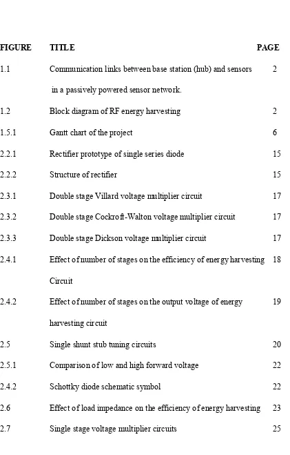
[image:18.595.139.470.623.715.2]Passively powered devices are increasingly important for a wide range of sensing applications. Also known as remotely powered devices, passively powered devices do not require any internal power source while extracting their power from propagating radio waves, sunlight, mechanical vibration, thermal gradients, convection flows or other forms of harvesting energy. One of the most popular power extraction methods for passively powered devices is to harvest power from propagating radio frequency (RF) signals. RF energy harvesting is a work of capturing ambient electromagnetic energy and converting into suitable DC power [10]. RF powered devices are typically used in applications such as structural monitoring where the RF powered devices are embedded into a structure making battery replacement impossible without destroying the structure (Figure 1.1). Some applications employing RF powered devices require deployment of these devices in very large numbers thus, making individual node battery replacement impractical.
Figure 1.1: Communication links between the base station (hub) and sensors in a passively powered sensor network, courtesy of [1]
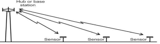
Figure 1.2 shows the block diagram of the energy harvesting system, where RF signals generated by multiple RF sources that will be captured by the antenna. The concept of harvesting DC power from RF signals is obtained from a combination of a receiving antenna and integrated to a rectifying circuit that efficiently converts RF energy to DC signals. Thus, RF energy harvesting is made up of a microwave antenna, a matching circuit with low pass filter, rectifying circuit, the next stage of low pass filter for DC path and a resistive load. The RF signals received by the antenna will be converted to DC signals by a diode based rectifying circuit. Depending on applications, a storage device could be introduced in order to efficiently utilize the DC power to charge the battery and depending on techniques it is enough to drive small electrical or low power consumption devices [1].
Figure 1.2: Block diagram of RF Energy Harvesting, courtesy of [1]
Besides that, RF energy harvesting also is a key technique can be employed in systems for generating some amount of electrical power to drive circuits in wireless communicating devices or, even so, to power supply a full node in wireless sensor networks (WSNs)[15]. There are some applications for wireless sensor network where earthquake detection is a part of them. Wireless sensor network
technology is produced in the earthquake disaster protection. A dynamic, real-time and changeful earthquake disaster wireless monitoring system is constructed so that it could meet each requirements of environmental monitoring which has great significance to the earthquake hazard prediction [13]. Then, this technology also makes a wide range of potential applications including precision agriculture, target tracking, temperature sensor and emergency relief. Such networks consist of a large number of distributed nodes and those nodes are expected to work independently in a very harsh environment [14].
1.2 Problem Statement
Finite electrical battery life is encouraging the companies and researchers come up with new ideas and technologies to drive wireless mobile devices for an infinite or enhanced period of time. Batteries add to size and their deposition causes environmental pollution. Thus, there is a growing demand for this technology because this energy harvesting technology presents a profitable future in low power consumer electronics and wireless sensor networks. Advancements in ultra low power or power-stingy electronics devices also a major driving factor for this type of technology [1]. A power source combined with energy harvesting can provide wireless devices for low maintenance cost and extended battery life, in place of conventional batteries with fixed energy storage, for point-to-point wireless communications. In addition to the challenge of transmitting the communication signal, a good rectifier which converts RF to DC signal, is needed so as to maximize the throughput. It should have high efficiency to convert as much of that energy as possible to use power. There are several researchers conducted studies on designing RF energy harvesting systems such as [1]-[19]. In particular for rectifier circuit
design, researches were concentrated on the efficient transmission and reception of high amounts of power, but in recent years the paradigm shifted to the capture of microwave radiation of relatively low power densities [18]-[19]. Previous researchers such as [11] and [15] also applied lump elements and conventional voltage multiplier to design the rectifier circuit. However, this kind of method is more complicated, and cannot produce high DC voltage. Thus, by using transmission line and active elements such as Schottky diode, rectifier with high DC-conversion voltage and optimum efficiency can be produced.
1.3 Objectives
The objective of this project is to develop high efficiency and low power consumption of RF-DC conversion for rectifier with an impedance matching circuit in RF energy harvesting system. In addition, the sub-objectives are stated as follows: a. To investigate the effect of rectifier stages as well as different load
impedance in rectifier circuit
b. To analyze the effect of matching network in rectifier circuit both for single and double stage rectifier
c. To fabricate and validate the design in the laboratory
1.4 Scope of Project
The main objective of this project is to design a rectifier with an impedance matching circuit for RF energy harvesting system. The first step in designing the process is to find and gather the information regarding to the project such as from journal and paperwork on the internet. This project will be focused on design and analysis as well as testing and measurement for rectifier with impedance matching circuit to improve the efficiency of RF energy harvesting. Agilent Advance Design System (ADS 2011) software will be used for the design process of rectifying with an impedance matching network. There are two stages of rectifier will be designed that is a single stage rectifier circuit and double stage rectifier circuit. First of all, the types of diode need to be selected for a very good performance of the diode can affect the overall performance of a rectifier circuit. Then, it will follow by the variations of the load where the load is varying from 100 Ω to 1 MΩ respectively. After that, the stub matching networks, which are included single and double stub matching also need to be designed in order to improve the performance of the rectifier circuit. After completing the design process, the next procedure is to fabricate the circuit and doing the testing and measurement procedure. Next, the result will be compared within the simulation result and the measurement result. Also, the combination between the rectifying circuits with antennas will be tested by using lab equipment to measure the performance of RF-DC conversion.
1.5 Methodology
1.5.1 Project Planning
One of the most important part of the project development is the project planning. A Gantt chart is prepared to help in implementing the project. The schedule is done in order to ensure all the progression of this project is well planned and organized. The schedule in the Gantt chart must be followed in order to make sure the project can be finished within the prescribed time. Figure 1.5.1 below shows the Gantt chart of this project.
Project Activities September October November December January February March April May June 1 2 3 4 5 6 7 8 9 10 11 12 13 14 15 16 17 18 19 20 1 2 3 4 5 6 7 8 9 10 11 12 13 14 15 16 17 18 Literature review
Study of rectifier topologies Design and simulation of single stage
rectifier with one diode and two diodes simultaneously Design and simulation of double stages rectifier with two diodes but different types of load impedance Report writing for PSM 1
Design and simulation of the integrated between rectifier and matching circuit
Tuning and optimization Fabrication Testing and measurement Report writing for PSM 2
E n d o f S em es t er B r ea k F in a l E x a m f o r S e me s t e r 1 S t u d y W e e k F in a l E x a m f o r S e me s t e r 2 S t u d y W e e k P S M b r ie f in g M id T e r m B b r e ak M id T e r m B r e ak 2013 2014 P S M B b r ie f in g
Figure 1.5.1: Gantt chart of the project
1.5.2 Data Collection
This project is started by the literature review process to study and learn about the RF-DC conversion efficiency enhancement that including the rectifier circuit and basic RF energy harvesting system. It was then followed by designing and developing the configuration by using ADS version 2011 software for a single stage and double stages rectifier with one and two diodes simultaneously, double stages with two diodes and different types of load impedances and rectifier integrated with matching circuit. When all the specification meets the requirement, the fabrication process of the rectifier circuit will be carried out were finalized design was fabricated with developing and etching technique, using FR4 substrate. Next the testing and measurement of the fabricated rectifier will be carried out, hence again will compare it with all the calculated and simulated results. The collected measurement data were extracted and analyzed followed by thesis report writing.
1.6 Contributions
The project outcomes were as follows:
a. The single and double stage rectifier with an impedance matching circuit for RF energy harvesting was designed. This new class of design provides excellent performance for the significant reduction in the costs associated with replacing batteries periodically as well as to provide wireless communication between electronic devices.
![Figure 1.2: Block diagram of RF Energy Harvesting, courtesy of [1]](https://thumb-us.123doks.com/thumbv2/123dok_us/137696.14840/19.595.138.539.424.576/figure-block-diagram-rf-energy-harvesting-courtesy.webp)
