This is a repository copy of Nano-scratch, nanoindentation and fretting tests of 5-80 nm ta-C films on Si(1 0 0).
White Rose Research Online URL for this paper: http://eprints.whiterose.ac.uk/84182/
Version: Accepted Version Article:
Beake, BD, Davies, MI, Liskiewicz, TW et al. (2 more authors) (2013) Nano-scratch,
nanoindentation and fretting tests of 580 nm taC films on Si(1 0 0). Wear, 301 (12). 575 -582. ISSN 0043-1648
https://doi.org/10.1016/j.wear.2013.01.073
© 2013, Elsevier. Licensed under the Creative Commons Attribution-NonCommercial-NoDerivatives 4.0 International http://creativecommons.org/licenses/by-nc-nd/4.0
eprints@whiterose.ac.uk https://eprints.whiterose.ac.uk/ Reuse
Unless indicated otherwise, fulltext items are protected by copyright with all rights reserved. The copyright exception in section 29 of the Copyright, Designs and Patents Act 1988 allows the making of a single copy solely for the purpose of non-commercial research or private study within the limits of fair dealing. The publisher or other rights-holder may allow further reproduction and re-use of this version - refer to the White Rose Research Online record for this item. Where records identify the publisher as the copyright holder, users can verify any specific terms of use on the publisher’s website.
Takedown
If you consider content in White Rose Research Online to be in breach of UK law, please notify us by
1
Nano-scratch, nanoindentation and fretting tests
of 5-80 nm ta-C films on Si(100)
B.D. Beake1,2,*, M.I. Davies1, T.W. Liskiewicz3, V.M. Vishnyakov2 and S.R. Goodes1
1
Micro Materials Ltd., Willow House, Ellice Way, Yale Business Village,
Wrexham, LL13 7YL, UK, Ben@micromaterials.co.uk
2
Dalton Research Institute, Manchester Metropolitan University,
Manchester M1 5GD, UK
3
Institute of Engineering Thermofluids, Surfaces & Interfaces, School of Mechanical
Engineering, University of Leeds, Woodhouse Lane, Leeds, LS2 9JT, UK
* Corresponding author, email: ben@micromaterials.co.uk
Abstract
Wear and stiction forces limit the reliability of Silicon-based micro-systems when mechanical
contact occurs. Ultra-thin filtered cathodic vacuum arc (FCVA) ta-C films are being
considered as protective overcoats for Si-based MEMS devices. Fretting, nano-scratch and
nanoindentation of different thickness (5, 20 and 80 nm) ta-C films deposited on Si(100) has
been performed using spherical indenters to investigate the role of film thickness, tangential
loading, contact pressure and deformation mechanism in the different contact situations. The
influence of the mechanical properties and phase transformation behaviour of the silicon
2
the ta-C film coated samples has been evaluated by comparison with previously published
data on uncoated Silicon. The small scale fretting wear occurs at significantly lower contact
pressure than is required for plastic deformation and phase transformation in nanoindentation
and nano-scratch testing. There is a clear correlation between the fretting and nano-scratch
test results despite the differences in contact pressure and failure mechanism in the two tests.
In both cases increasing film thickness provides more load support and protection of the Si
substrate. Thinner films offer significantly less protection, failing at lower load in the scratch
test and more rapidly and/or at lower load in the fretting test.
1. Introduction
Wear and stiction forces limit the reliability of Silicon-based micro-systems (e.g. MEMS)
when mechanical contact occurs [1-3]. Silicon exhibits highly complex mechanical and
tribological behaviour with phase transformations and lateral cracking observed in
indentation and brittle fracture in a wide range of mechanical contacts [4-6]. It exhibits little
or no conventional plasticity at room temperature and its deformation is dominated by phase
transformation and fracture. Its nanoindentation behaviour has been extensively studied
[7-12]. It has been established that a phase transformation to metallic behaviour occurs beneath
the contact site and the pop-out during unloading is a consequence of phase transformation
and volumetric expansion. Less well studied is its behaviour under the type of more complex
loading geometries that can occur in practical tribological situations [13] so we recently
investigated the behaviour of highly polished Si(100) under different contact situations, using
a nanomechanical test system to perform nanoindentation, nano-scratch and 10000 cycle
small scale fretting tests all with the same 4.6 m sphero-conical diamond indenter [14-15].
Tangential loading in the nano-scratch and fretting tests promoted non-elastic yield at lower
critical load. Silicon showed subtle rate sensitivity in the nano-scratch and nanoindentation
3
initial loading. When the load was applied abruptly in <0.3 s, radial and lateral cracking and
material removal was observed and large displacement jumps (pop-ins) were observed during
the subsequent fretting test. In contrast, when the load was applied more slowly in 10 s radial
cracking was not observed and there was a distinct threshold load at around 100 mN marking
the transition to a more severe wear mode with extensive lateral cracking and material
removal.
Several approaches are being considered including liquid lubrication [16], and solid
lubrication with self-assembled monolayers [17], ALD [18, 19] and carbon films [20-23].
Particularly promising results on actual MEMS devices have been obtained for conformal
deposition strategies (WS2 by ALD [19], DLC by PECVD [20]). Tetrahedral amorphous
carbon (ta-C) films deposited by FCVA have been developed for MEMS applications
including capacitive sensors and protective coatings for micromachined components [21-23].
The mechanical and interfacial behaviour of the contacting silicon surfaces is modified by
these thin, low surface energy films. Nanoindentation with a Berkovich indenter has shown
that the films are hard (hardness of 80 nm ta-C is ~22 GPa) and elastic [24-25]. This high
hardness and H/E is due to >70% sp3 [26] but the films can be highly stressed if deposited to
too great thickness [27-28]. Nano-scratch testing of ta-C films has shown that they are
sufficiently thin to not show large area delamination and scratch resistance increases with
H/E [24-25]. Increasing the ta-C thickness from 5 to 80 nm was found to increase the critical
load for film delamination by a factor of two.
In this current study nanoindentation and nano-scratch tests have been performed on 5, 20
and 80 nm ta-C films with a 4.6 µm radius probe, and fretting with 5 and 37 µm probes to
determine (i) rate sensitivity of pop-outs during unloading in nanoindentation (ii) whether the
4
the extent of rate sensitivity in film failure in the nano-scratch test (iv) the influence of the
ta-C on lateral cracking thresholds in nano-scratch testing (v) the mechanism of film failure in
the fretting test and the influence of film thickness on the fretting wear. The influence of the
mechanical properties and phase transformation behaviour of the silicon substrate in
determining the tribological performance (critical loads, damage mechanisms) of the ta-C
film coated samples has been investigated by comparison with previously published [14-15]
data on uncoated Silicon acquired with the same probe and experimental conditions.
2. Experimental
Nanoindentation and nano-scratch tests were performed on ta-C films deposited on silicon
wafers with a commercial ultra-low drift nanomechanical test system (NanoTest, Micro
Materials Ltd.) fitted with a 4.6 m end radius sphero-conical diamond indenter which was
calibrated by nanoindentation measurements on a fused silica reference sample over a wide
load range. ta-C films of 5, 20 and 80 nm thickness were deposited on Si(100) substrates by
FCVA [24-25]. The substrates were ultrasonically cleaned with deionized water for 10 min,
followed by drying with a static neutralizing blow off gun. The samples were placed in the
deposition chamber of an industrial filtered cathodic vacuum arc system (Nanofilm
Technologies Pte. Ltd.) evacuated to a base pressure lower than 1 x 10⁻⁶ torr. Prior to
deposition, the silicon surface was sputtered by an argon ion beam from a dc ion beam source
for 3 min to remove the native oxide. The substrate holder was in floating bias. The film
thickness of the 20-80 nm films was measured by a surface profiler and the thickness of the 5
nm film was estimated from the deposition rate. The Ra surface roughness was 1.8, 2.1 and
3.1 nm for the 5, 20 and 80 nm films respectively [24]. The influence of the films on the
5
uncoated highly polished 300 m thick Si(100) wafer provided by PI-KEM (Tamworth, UK)
using the same 4.6 m sphero-conical diamond indenter.
Three repeat indentation tests to 10, 50, 100, 200, 300, 400, 500 mN peak load, loading and
unloading in 20 s, with a 5 s hold at peak load were performed on the 5, 20 and 80 nm films.
Further tests were performed on the 80 nm ta-C to a range of peak loads and unloading rates
with a 5 s hold at peak load:- (i) Peak load = 100 mN, loading rate = 5 mN/s; unloading rate =
1-50 mN/s, 10 repeats for each unloading rate; (ii) Peak load = 200 mN, loading rate = 10
mN/s; unloading rate = 1-50 mN/s, 20 repeats for each unloading rate. In all tests a 60s hold
at 90% unloading was used to correct the data for (any) thermal drift.
Nano-scratch tests to 200 mN were performed on the 80 nm ta-C film tests over a wide range
of loading rates (dL/dt = 0.1-12 mN/s) and scan speeds (dx/dt = 0.1-40 m/s) to provide
critical load data over a range of dL/dx = 0.1-100 mN/m. 1-5 repeat tests were performed
for each set (11 in total) of experimental conditions. Tests were performed as multi-pass
(3-scan) experiments (topography-scratch-topography) that were subsequently analysed in the
NanoTest software to determine the on-load and residual depth data, following the procedure
described in reference 18. Additional scratch tests were carried out on the ta-C films and
uncoated Si(100) to a peak load of 300 mN with a loading rate of 12 mN/s and scanning
speed 10 m/s to investigate lateral cracking (3 repeats on Si, 5 on the ta-C films). All tests
were spaced at least 50 m apart.
The fretting tests were performed in a NanoTest Vantage system using 5 and 37 m diamond
probes whose end radii were calibrated by nanoindentation testing over a wide load range on
6
includes an additional oscillating stage with a multi-layer piezo-stack to generate sample
motion. The piezo movement is magnified by means of a lever arrangement to achieve larger
amplitudes [29]. The fretting track length was set at 10 m and the oscillation frequency 5
Hz. Fretting experiments of differing number of wear cycles and applied load were performed
in normal laboratory conditions (~50 % RH) on the ta-C films as summarised in Table 1. The
mean initial Hertzian contact pressures in the tests ranged from ~3-4 GPa at 10 mN to ~10
GPa at 200 mN using the 37 m probe and were ~6 GPa using the 5 m probe. Adjacent tests
were spaced 100 m apart. Tangential (friction) force data were acquired simultaneously with
depth data throughout the nano-scratch and fretting tests using a lateral force transducer
7
Table 1 Fretting test experimental conditions
5 nm ta-C 20 nm ta-C 80 nm ta-C
R = 37 m, L = 1 mN 900 cycles
R = 37 m, L = 10 mN 300, 600, 900,
1500, 3000, 6000,
9000, 18000 cycles
1500, 3000, 6000,
9000, 18000 cycles
R = 37 m, L = 50 mN 300, 600, 900,
1500, 3000, 6000,
9000 cycles
1500, 3000, 6000,
9000, 18000
cycles
R = 37 m, L = 200 mN 300, 600, 900,
1500, 3000, 6000,
9000, 18000
cycles
R = 5 m, L = 10 mN 1500, 3000, 6000,
9000, 18000
cycles
The Electron microscopy was done utilising Zeiss Supra 40 VP (variable pressure) electron
microscope. Secondary electron imaging was done by conventional (Everhart-Thornley) and
In-Lens secondary electron detector. The detectors have different sensitivity to the surface
charge and topography, when In-Lens detector is more sensitive to surface charging and less
sensitive to topography. Surface charging can be caused by the surface enrichment with
oxygen (oxidation) and this was utilised in this communication. Backscattering is strongly
affected by average atomic number when heavier species, like silicon, have higher
8
this paper, part of the backscattering signal is coming from top carbon layer and part of the
signal from silicon. If across the scan view the thickness of carbon varies, then more signal is
coming where carbon thickness is less. The Silicon Drift Detector from EDAX was used to
obtain qualitative results of film composition and thickness. The results were obtained at 5
keV electron beam in order to increase top layer sensitivity. Fully quantitative results in the
situation with the variable composition and thickness films on a substrate can only be
obtained in conjunction with modelling and will be published later. The line scans presented
in the paper can be used for the qualitative analysis.
3. Results
3.1 Nanoindentation
Figure 1 (a) shows illustrative nanoindentation curves to 500 mN on all of the samples. Large
pop-ins (extensive lateral cracking) were observed occasionally at >400 mN, as in one of the
tests shown on the 80 nm ta-C, but there was no obvious dependence of the critical loads
required on film thickness. Figure 1 (b) shows typical nanoindentation curves to 100 mN on
the 80 nm film and uncoated Si(100). At low load the curves are elastic and virtually identical
as both are due to the elastic behaviour of the Silicon. As the load increases small but clear
differences are observed with pop-ins on Si at ~37 mN, at ~43 mN on the 80 nm film and an
additional pop-in at higher load, more obviously on the ta-C film at ~76 mN. The pop-out
during unloading occurs at higher load on the uncoated Si. Figure 1 (c) shows the variation in
pop-out load after unloading from 100 or 200 mN at 1-50 mN/s together with previously
reported [15] data on Si(100) acquired with the same probe and experimental conditions for
comparison. Pop-ins are less clear in the 200 mN tests where loading was at 10 mN/s than in
9
[image:10.595.86.522.81.458.2]10
Figure 1 (b) Typical nanoindentation curves to a peak load of 100 mN on Si (thicker line) and
80 nm ta-C (thinner line). Unloading rate = 2.5 mN/s. The pop-ins during loading are marked
[image:11.595.72.527.67.461.2]11
Figure 1 (c) Variation in critical load for pop-out with unloading rate on Si (filled symbols)
and 80 nm ta-C (open symbols). The peak load was 200 mN for the circles and 100 mN for
the triangles.
3.2 Nano-scratch
The films exhibited the expected critical load transitions as the load increased. A depth trace
from a typical test is shown in figure 2 (a). The data shown has been corrected for
topography, sample slope and instrument compliance following the procedure described in
[image:12.595.82.527.77.448.2]12
scanning force (after load removal). In this example the onset of non-elastic behaviour (Ly)
occurs after 136 m (44 mN). At Lc1 (192 m, 71 mN) there is step in the residual depth data
and total film failure occurs a depth change of just over 80 nm at Lc2 (266 m, 108 mN).
Backscattered SEM images confirm total film failure and substrate exposure at this point (e.g.
insert in figure 2 (b)).
Figure 2 (a) Nano-scratch behaviour of the 80 nm ta-C film. Loading rate = 1 mN/s. Scan
speed = 2 m/s.
On the 80 nm ta-C clear film failure (Lc2) was observed in all the tests to 200 mN but lateral
cracking (Lc3) was absent. Above the critical load for edge cracking, Lc1, but prior to the total
[image:13.595.74.526.223.552.2]13
track. SEM images (e.g. figure 2 (b)) show periodic cracking across the scratch track between
Lc1 and Lc2. At film failure the abrupt change in depth is very close to the film thickness.
Figure 2 (b). SEM image of the scratch on the 80 nm ta-C film shown in figure 2 (a) showing
Lc2 failure preceded by cracking across the scratch track (main image = SE image, insert =
back-scatttered image). The scratch direction (left to right) is shown by an arrow on the SE
[image:14.595.71.530.136.442.2]14
Figure 2 (c) Variation in the critical load for film failure (Lc2) in the nano-scratch test with
dL/dx for the 80 nm ta-C film.
Table 2 Critical load for lateral cracking in nano-scratch tests
Si 5 nm ta-C 20 nm ta-C 80 nm ta-C
Lc3 (mN) 130 ± 10 152 ± 35 163 ± 45 276 ± 20
Figure 2 (c) shows the variation in Lc2 vs. dL/dx for the 80 nm ta-C film. Friction coefficients
[image:15.595.79.527.74.469.2]15
cracking. The variation in the critical load for lateral cracking with film thickness is shown in
Table 2. The critical load for the Lc3 failure increased dramatically on the 80 nm ta-C and the
lateral cracking was less pronounced. For the uncoated, 5 and 20 nm ta-C film sample the
[image:16.595.77.524.200.458.2]scratch track is more jagged after Lc3 due to the more extensive lateral cracking (figure 3).
Figure 3. Optical micrographs of nano-scratches to 300 mN on (a) uncoated Si, (b) 5 nm ta-C,
(c) 20 nm ta-C and (d) 80 nm ta-C films. The onset of lateral cracking (Lc3 failure) is marked
by an asterisk.
3.3 Fretting and SEM/EDX analysis of fretting scars
The on-load probe depth did not show abrupt steps during the fretting tests, more typically
showing an initial slight decrease before a transition point after which it increased
progressively through the test. The point marking the onset of the increase in depth was
16
typically (0.10 ± 0.01). In the fretting of the 20 nm ta-C film at 50 mN the friction and
on-load depth signals show a transition occurring at >1500 cycles. SEM/EDX analysis of the
fretting tests stopped after 1500 and 3000 cycles was performed to investigate the behaviour
[image:17.595.78.522.193.533.2]in more detail (figure 4).
Figure 4. SEM imaging of wear scars after fretting the 20 nm ta-C film at 50 mN for 1500
cycles (a = SE image, b = scatttered image) and 3000 cycles (c = SE image, d =
17
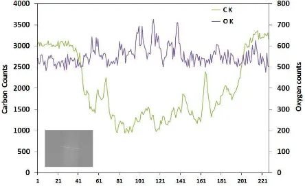
Figure 5. EDX line profile across the wear scar corresponding to the 1500 cycle test shown in
figure 4 (a-b).
EDX line profiles across the fretting wear scar of the 1500 cycle test revealed thinning of the
20 nm film and oxygen incorporation in the worn region (figure 5). The worn scar of the
3000 cycle test showed more oxygen incorporation in the track and in the debris particles
together with some exposed Silicon due to removal of the film and the C signal dropped to
zero. 300 cycle tests also showed reduction in coating thickness and oxygen incorporation.
Similar behaviour was observed on the 5 nm film at 10 mN with oxygen incorporation and
film thinning within 1500 cycles and complete removal of the film from the wear scar region
in the 3000 cycle test. EDX analysis of short duration fretting wear scars on the 80 nm ta-C
film did not show the same oxygen incorporation as on the thinner films. For the 80 nm film,
at 200 mN with the 37 µm probe, the total film failure occurs between 3000 and 6000 cycles.
18
number of cycles than the 80 nm film, and at 10 mN similarly the 5 nm film is worn away
more rapidly than the 20 nm film. Wear scars from 18000 cycle tests on the 80 nm ta-C
showed a reduction in track length at 200 mN compared to 50 mN.
4. Discussion
The presence of the ta-C film affects the phase transformation behaviour of the Si by
providing load support, reducing the effective load reaching the substrate and spreading the
deformation out over a wider area. Critical loads for pop-ins and pop-outs are modified by the
presence of the ta-C overlayer. While their exact positions change, the rate dependence of
them is virtually identical with and without the ta-C (e.g. see figure 1(iii)) confirming that
they are due to transitions in the underlying Si rather than the film. It is interesting to
compare and contrast this behaviour with that observed for thicker films. Haq and co-workers
used SEM, focussed ion beam microscopy (FIB) and cross-sectional transmission electron
microscopy (XTEM) techniques to investigate the deformation occurring in indentation
contacts with a 5 µm probe for Si coated with 1.6 µm RF a-C:H [30], 600 nm RF a-C:H [31]
and a 30 GPa 170 nm FCVA ta-C [26]. For the 1.6 µm a-C:H they found that at 100 mN the
coating showed a reduction in thickness of ~4.5 % but there was no deformation at the
interface or in the substrate and phase transformation was suppressed. At 100 mN on the 600
nm a-C:H film they observed 4.4% compressive strain in the coating, some bending at the
interface with some slight delamination and some plastic deformation accompanied phase
transformation. From the presence of slip without transformed material at 50 mN they
suggested therefore that plastic deformation in the Si rather than phase transformation or any
coating cracking was responsible for the first pop-in. For the 170 nm ta-C film they observed
19
pop-ins at 12-18 mN and phase transformation and cracking at higher loads. Even though the
indentation depth at 10 mN was over 50 % of the film thickness XTEM showed no evidence
for plastic compression of the coating, only some bending at the interface. As with the thicker
film, the first critical load at ~15 mN was assigned to slip in the Si and the second at ~24 mN
to phase transformation. Although the 170 nm ta-C film was harder (30 GPa) than the 80 nm
ta-C, Haq et al reported a penetration depth at 10 mN of ~100 nm which could suggest that
the radius of the tip was actually considerably less than the nominal 5 µm and/or it has
developed some asperity damage at the tip. This would provide an explanation of why the
critical loads in that study were observed at much smaller loads than in all of the reported
tests on Si(100) with 4.2-5.0 µm indenters [7,8,15,32]. In the current work with a 4.6 µm end
radius probe the on-load indentation depth was only ~75 nm for all the ta-C films and we did
not see any critical loads until ~44 mN. Although it is conceivable that the first pop-in in the
80 nm film/Si system is a result of plastic deformation phase transformation is at least as
likely, as indentations to 50 mN on the 80 nm ta-C show an elbow event (phase
transformation) in unloading at ~10 mN. For uncoated Si, the first pop-in – which XTEM
shows is due to phase transformation - occurs around 40 mN with this 4.6 µm probe,
consistent with reported values of 28 mN with a 4.2 µm probe [7,8] and 37 mN with a 5 µm
probe [32]. On uncoated Si phase transformation (elbowing) during unloading was observed
on unloading from 55-65 mN.
Nevertheless, some localised slip may occur at low load in the 80 nm ta-C system; evidence
for the influence of the film in initially retarding phase transformation but promoting slip in
the substrate is provided by the presence of in the much larger pop-out that occurs on the film
at around 70-85 mN than on the uncoated Si where a smaller pop-out occurs at ~80-95 mN. It
seems reasonable to assume that this is phase transformation. In unloading from 100 mN
20
Since the rate dependence is virtually identical with and without the film, it is clear that these
relate to the same process in the silicon, with the presence of the ta-C film retarding the
pop-outs, as has been observed for thicker systems and in our own work with a sharper Berkovich
indenter where the mean pop-out load unloading from a peak load of 20 mN at 0.5 mN/s
decreased from 4.7 mN on the uncoated Si to 4.0 mN and 3.3 mN for 20 nm and 80 nm ta-C
respectively [24].
The influence of film thickness and indenter radius on the critical loads for yield, edge
cracking and total film failure in the nano-scratch test have been extensively studied
previously. With a 3.1 µm end radius probe a contact pressure of about 12 GPa was required
for yield on the 5, 20 and 80 nm films. Hertzian analysis of contact pressure at failure using
the 4.6 µm probe gives a contact pressure of (15 ± 1) GPa for the 80 nm film at Lc2, which is
close to the value of 14.5 GPa previously determined with the 3.1 µm probe. Chang and
Zhang have reported that in Berkovich indentation of uncoated Si (100) the critical load for
pop-in is around 14 GPa, close to a theoretical value of 14.3 GPa for the transition from Si-I
to Si-II under spherical indentations [11]. They therefore interpreted the inelastic deformation
as being solely due to phase transformation. After the pop-in the contact pressure dropped to
~12 GPa, i.e. the hardness of silicon. Although tangential loading promotes yield (as
described in [15] for uncoated Si(100)) the contact pressures in indentation and nano-scratch
of Si or coated Si are not that different as the friction at yield is low.
Here we were also interested in the lateral cracking (Lc3 failure) that occurs on Si at higher
load and whether the ta-C films could protect the substrate or not. The nano-scratch test data
show that tangential loading promotes the formation of large lateral cracks on all the ta-C
film samples at much lower load than in nanoindentation as was recently observed for
uncoated Si(100) [15]. The occurrence of large pop-ins at high load when Silicon is indented
co-21
workers reporting a threshold load of (350 ± 100) mN with a 4.3 µm probe and larger pop-ins
(>1 µm) more likely at >500 mN [33]. In the limited number of high load nanoindentation
tests performed the thin hard ta-C films showed no significant protection against lateral
cracking, which occurred only occasionally, irrespective of the ta-C film thickness. However,
in the nano-scratch test the tangential loading promoted dramatic film failure at much lower
load (e.g. ~115 mN for 80 nm ta-C; see figure 2) with extensive lateral cracking occurring
below 300 mN. Marked differences emerged for the 80 nm film where the critical load for
this Lc3 failure increased dramatically and the lateral cracking was less pronounced. These
thin films do not show any of the large-area delamination outside the scratch track commonly
observed on failure of thicker hard and elastic (high H/E) coatings [34]. It appears that when
the film fails in the scratch track, the intact ta-C film outside the scratch track is capable of
maintaining a measure of load support and providing some protection.
Although, as expected for a brittle material, Silicon has been shown to be very rate sensitive
in rapid (<0.3 s) loading [14] or at high sliding speeds [35], in our previous study of the rate
dependence of its behaviour in the nano-scratch test [15] we noted only a small dependence
of the critical load on dL/dx, which was consistent with similarly small kinetic effects on the
phase transformation events observed in nanoindentation testing with the same probe.
Nano-scratch tests on the 80 nm ta-C film on Si have been performed over a much wider range of
dL/dx in the current study revealing minimal rate dependence, with the critical load for film
failure being (113 ± 15) mN over a 100-fold variation in dL/dx from 0.1-100 mN/m. This
very small rate-sensitivity in the scratch response is consistent with previous studies of a-C:H
and a-C:H/Si films on glass which showed no obvious rate sensitivity over a 20-fold range of
dL/dx from 0.05-1 mN/m [36]. The increase in friction force with load follows closely the
behaviour observed on uncoated Si. In both cases this is due to increasing ploughing
22
was observed by Sundararajan and Bhushan in AFM-nanoscratching, where friction
coefficients on 3.5-20 nm ultra-thin carbon films were initially 0.04-0.06, which was the
same as Si(100) tested under the same conditions, increasing to ~0.1 at the critical load
[37,38]. Liu et al reported that graphitic layers at the surface (~3 nm) were responsible for
lower friction coefficients of ~0.09 on ta-C than other a-C:H films [39]. Tangential loading
with friction can promote yield, with the magnitude of the decrease depending on the friction
as shown by Zok and Miserez [40]. Blees and co-workers reported that the critical load in
scratching sol-gel coatings on polypropylene decreased by an order of magnitude when the
friction increased from 0.5 to 3 [41]. However, the friction coefficient is only 0.07 at yield on
Si so the effect was rather small, with critical loads for yield (first pop-in) being (40 ± 5) mN
in indentation and (37 ± 5) mN in nano-scratch. Wu and co-workers noted a reduction in the
critical load for phase transformation in nano-scratching compared to nanoindentation [42].
As the friction coefficient at yield of the ta-C films is only 0.09, it is unsurprising that there
was little difference in the critical load for yield in the nano-scratch test being generally no
lower than in nanoindentation.
In the fretting test deformation proceeds by a fatigue mechanism with a gradual wearing
away of the film, as shown by the EDX profiles across scars, and the absence of any abrupt
changes in depth or friction. Li and Bhushan reported that fatigue wear and fatigue-induced
delamination occur in reciprocating sliding of ta-C films depending on film thickness [43].
Wilson and Sullivan reported a similar process in nano-fretting of 10-150 nm a-C films
deposited on Si by closed field unbalanced magnetron sputter ion plating (CFUBMSIP)
[44-46]. This fatigue wear process is in marked contrast to the behaviour in the nano-scratch test
where the contact pressure is greater and distinct critical loads are observed, with abrupt
increases in probe depth and friction. Appreciable substrate deformation and bending at the
23
failure are significantly lower in the fretting test due to lower substrate deformation and
consequently the friction force at failure is lower in the fretting test due to a smaller
contribution from ploughing. A similar friction coefficient (0.09-0.12) was found by Qian
and co-workers in low-cycle nano-fretting of NiTi shape memory alloy with a 50 m
diamond when the contact pressure was sufficiently low that ploughing was minimized [47].
Hertzian analysis can be used to estimate the contact pressure at the start of the reciprocation
in the fretting tests assuming initially elastic contact. For the 37 µm probe this gives ~3-4
GPa at 10 mN, ~8 GPa at 50 mN and 9-11 GPa at 200 mN. For the 5 µm probe this gives ~6
GPa. The on-load probe depth data typically show a small reduction during the first wear
cycles which may be due to blistering, delamination, phase transformation and oxygen
incorporation. Hillocks have been shown to form at contact pressures > 1 GPa in
nano-fretting tests in an AFM on Si(100) [48] and volume uplift due to the phase transformation of
the underlying Si may be occurring here. Hard carbon films are known to suffer from poor
adhesion and delamination-induced blistering, and in repetitive spherical nanoindentation of
500 nm DLC films on Si(100) blistering and delamination of the film resulted in a reduction
of indentation depth with loading cycles when a spherical indenter was used [49].
Li and Bhushan proposed a mechanism for fatigue failure of 3.5-20 nm ta-C films in
reciprocating sliding with 3 mm sapphire sliders. In this mechanism wear fatigue cracks form
in the coating and on thinner (3.5, 5 nm ta-C) propagate to the interface resulting in
delamination but for 20 nm do not reach the interface. We have previously noted that this
mechanism does not take into account substrate deformation and interface bending and
therefore is not directly applicable to the behaviour in the nano-scratch test where appreciable
elastic and plastic substrate deformation occurs and failure does not occur until the probe
24
failure is closer to that proposed by Li and Bhushan although some substrate deformation
does occur.
Analysis of the SEM images of fretting wear scars revealed distinctive gross-slip type of
damage with scratches generated during sliding present within the wear scar area. The
damage mechanics of ta-C films seems to be progressive wear by debris generation and
debris aggregation outside the contact area. Wang and Kato observed transitions from
no-wear to a no-wear particle regime in low cycle pin on disk testing of CNx coatings in an SEM
over the contact pressure range 5-18 GPa [50]. At low load initially only “feather-like”
particles were produced and with increasing wear cycles a transition to “plate-like” particles
was found [50]. In macro-scale reciprocating wear of Si [43,51] or ta-C films [52] a
significant running in period of high friction has been reported. This has been interpreted as
adhesive wear resulting from the low real area of contact and high local stresses. Fretting
wear particles were generated and as the test progressed a transition to flake morphology and
deep grooves in the wear track due to abrasive wear was observed. In the nano-scale tests the
running-in period was much shorter. As a result of using 37 µm radius probe rather than 5
µm, no cracking or coating delamination, as observed in the case of nano-scratch test, has
been observed around fretting wear scars even under maximum load of 200 mN. The
geometry of the wear scars correlated with the loads applied and wider wear tracks were
observed as a result of higher contact pressures and larger Hertzian contact radius. The
reduction in wear track length with increased load from 50 to 200 mN on the 80 nm ta-C is
consistent with other studies of small-scale fretting [53]. EDX analysis confirmed coatings
perforation for longer tests with EDX line scans showing higher oxygen content and lower
carbon counts due to thinning of coatings. Low cycle tests showed coating thinning and
corresponding oxide formation even after short 300-cycle experiments. Oxygen incorporation
25
indicated oxidation as a possible mechanism in the sliding wear of ta-C films [54]. With the 5
µm probe the 80 nm ta-C film wears readily at a much lower load of 10 mN. The maximum
von Mises stress is well into the substrate (at a depth ~260 nm) and the applied load below
that required for Si phase transformation. Fretting damage may be initiated by micro-slip in
the substrate, as has been shown in low load indentations of 170 nm ta-C films. Phase
transformation is expected to play a key role since De-kun and co-workers have shown that
ion implantation of Si(111) significantly improved its wear resistance in a reciprocating wear
test [51], presumably as the amorphous near-surface layer formed did not undergo phase
transformations in contact in the same way.
5. Conclusions
The presence of the ta-C film affects the phase transformation behaviour of the Si by
providing load support, reducing the effective load reaching the substrate and spreading the
deformation out over a wider area. Critical loads for pop-ins and pop-outs are modified by the
presence of the ta-C overlayer. While their exact positions change, the rate dependence of
them is virtually identical with and without the ta-C confirming that they are due to
transitions in the underlying Si rather than the film. The nano-scratch test data show that
tangential loading promotes the formation of large lateral cracks on all the ta-C film samples
at much lower load than in nanoindentation. Increasing the ta-C film thickness to 80 nm
significantly increased the critical load for this lateral cracking. Small scale fretting wear
occurs at significantly lower contact pressure than is required for plastic deformation and
phase transformation in nanoindentation and nano-scratch testing. There is a clear correlation
between the fretting and nano-scratch test results despite the differences in contact pressure
and failure mechanism in the two tests. In both cases increasing film thickness provides more
26
protection, failing at lower load in the scratch test and more rapidly and/or at lower load in
the fretting test.
6. Acknowledgements
Experimental assistance from Nick Pickford (Micro Materials Ltd), provision of test samples
from Professor Daniel Lau (Nanyang Technological University, Singapore) and funding from
the Welsh Assembly Government Single Investment Fund are gratefully acknowledged.
7. References
1. J.A. Williams and H.R. Le, Tribology and MEMS, J. Phys. D: Appl. Phys. 39 (2006)
R201-R214.
2. D.M. Tanner, W.M. Miller, W.P. Eaton, L.W. Irwin, K.A. Peterson, M.T. Dugger et
al, The effect of frequency on the lifetime of a surface micromachined microengine
driving a load, 1998 IEEE International Reliability Physics Symposium Proceedings,
March 30 – April 2, 1998, pp. 26-35.
3. I.S.Y. Ku, T. Reddyhoff, A.S. Holmes, H.A. Spikes, Wear of silicon surfaces in
MEMS, Wear 271 (2011) 1050-1058.
4. R.F. Cook, Strength and sharp contact fracture of silicon. J. Mater. Sci. 41 (2006) 841.
5. S. Bhowmick, H. Cha, Y.-G. Jung, B.R. Lawn, Fatigue and debris generation at
indentation-induced cracks in silicon, Acta. Mater. 57 (2009) 582-589.
6. V. Domnich, Y. Gogotsi, Phase transformations in silicon under contact loading, Rev.
Adv. Mater. Sci. 3 (2002) 1-36.
7. J.E. Bradby, J.S. Williams, J. Wong-Leung, M.V. Swain, P. Munroe, Mechanical
deformation of crystalline silicon during nanoindentation, Mat. Res. Soc. Symp. Proc.
27
8. J.E. Bradby, J.S. Williams, J. Wong-Leung, M.V. Swain, P. Munroe, Mechanical
deformation in silicon by microindentation, J. Mater. Res. 16 (2001) 1500-1507.
9. T. Juliano, Y. Gogotsi, V. Domnich, Effect of indentation unloading conditions on
phase transformation induced events in silicon, J. Mater. Res. 18 (2003) 1192-1201.
10.T. Juliano, V. Domnich, Y. Gogotsi, Examining pressure-induced phase
transformations in silicon by spherical indentation and raman spectroscopy: A
statistical study, J. Mater. Res. 19 (2004) 3099-3108.
11.L. Chang, L.C. Zhang, Deformation mechanisms at pop-out in monocrystalline silicon
under nanoindentation, Acta. Mater. 57 (2009) 2148-2153.
12.L. Chang, L.C. Zhang, Mechanical behaviour characterisation of silicon and effect of
loading rate on pop-in: A nanoindentation study under ultra-low loads, Mater. Sci.
Eng. A 506 (2009) 125-129.
13.A. Matthews, S. Franklin, K. Holmberg, Tribological coatings: contact mechanisms
and selection, J. Phys. D: Appl Phys. 40 (2007) 5463-5475.
14.B.D. Beake, T.W. Liskiewicz, N.J. Pickford, J.F. Smith, Accelerated nano-fretting
testing of Si(100), Tribol. Int. 46 (2012) 114-118.
15.B.D. Beake, T.W. Liskiewicz and J.F. Smith, Deformation of Si(100) in spherical
contacts – comparison of nano-fretting and nano-scratch tests with nanoindentation,
Surf. Coat. Technol. 206 (2011) 1921-1926.
16.I.S.Y. Ku, T. Reddyhoff, R. Wayte, J.H. Choo, A. S. Holmes, H.A. Spikes,
Lubrication of microelectromechanical devices using liquids of different viscosities, J.
Tribol. 134 (2012) 012002-1.
17.R. Maboudian, W.R. Ashhurst, C. Carraro, Self-assembled monolayers as anti-stiction
coatings for MEMS: characterisation and recent developments, Sensors Actuators, 82
28
18.C. Nistorica, J.-F. Liu, I. Gory, G.D. Skidmore, F.M. Mantiziba, B.E. Gnade et al, J.
Vac. Sci. Technol. A 23 (2005) 836.
19.T.W. Scharf, S.V. Prasad, M.T. Dugger, P.G. Kotula, R.S. Goeke and R.K. Grubbs,
Growth, structure, and tribological behaviour of atomic layer-deposited tungsten
disulphide solid lubricant coatings with applications to MEMS, Acta Mater. 54 (2006)
4731-4743.
20.S.A. Smallwood, K.C. Eapen, S.T. Patton and J.S. Zabinski, Performance results of
MEMS coated with a conformal DLC, Wear 260 (2006) 1179-1189.
21.N. Akita, Y. Konishi, S. Ogura, M. Imamura, Y.H. Hu and X. Shi, Comparison of
deposition methods for ultra thin DLC overcoat film for MR head, Diamond Relat.
Mater. 10 (2001) 1017-1023.
22.C.Y. Chan, K.H. Lai, M.K. Fung, W.K. Wong, I. Bello, R.F. Huang, C.S. Lee, S.T.
Lee and S.P. Wong, Deposition and properties of tetrahedral amorphous carbon films
prepared on magnetic disks, J. Vac. Sci. Technol. A 19 (2001) 1606.
23.Shi, B.K. Tay, H.S. Tan, L. Zhong, Y.Q. Tu, S.R.P. Silva and W.I. Milne, Properties
of carbon ion deposited tetrahedral amorphous carbon films as a function of ion
energy, J. Appl. Phys. 79 (1996) 7234-7240.
24.B.D. Beake, S.P. Lau, Nanotribological and nanomechanical properties of 5-80 nm
tetrahedral amorphous carbon films on silicon, Diam. Relat. Mater. 14 (2005)
1535-1542.
25.B.D. Beake, S.R. Goodes, B. Shi, Nanomechanical and nanotribological testing of
ultra-thin carbon-based and MoST films for increased MEMS durability, J. Phys. D:
29
26.A.J. Haq, P.R. Munroe, M. Hoffman, P.J. Martin, A. Bendavid,
Nanoindentation-induced deformation behaviour of tetrahedral amorphous carbon coating deposited by
flitered cathodic vacuum arc, Diam. Relat. Mater. 19 (2010) 1423-1430.
27.D. Sheeja, B.K. Tay, K.W. Leong and C.H. Lee, Effect of film thickness on the stress
and adhesion of diamond-like carbon coatings, Diam. Relat. Mater. 11 (2002)
1643-1647.
28.D. Sheeja, B.K. Tay, S.P. Lau, K.W. Leong and C.H. Lee, An empirical relation for
critical load of DLC coatings prepared on silicon substrates, Int. J. Mod. Phys. B 16
(2002) 958-962.
29.T.W. Liskiewicz, B.D. Beake, J. F. Smith, In situ accelerated micro-wear – a new
technique to fill the measurement gap, Surf. Coat. Technol. 205 (2010 1455-1459.
30.A.J. Haq, P.R. Munroe, M. Hoffman, P.J. Martin, A. Bendavid,
Nanoindentation-induced deformation behaviour of diamond-like carbon coatings on silicon substrates,
Thin Solid Films 515 (2006) 1000-1004.
31.A.J. Haq, P.R. Munroe, M. Hoffman, P.J. Martin, A. Bendavid, Effect of coating
thickness on the deformation behaviour of diamond-like carbon-silicon system, Thin
Solid Films 518 (2010) 2021-2028.
32.E.R. Weppelmann, J.S. Field, M.V. Swain, J. Mater. Sci. 30 (1995) 2455.
33.D.J. Oliver, B.R. Lawn, R.F Cook, M.G. Reitsma, J.E. Bradbury, J.S. Williams et al,
Giant pop-ins in nanoindented silicon and germanium caused by lateral cracking, J.
Mater. Res. 23 (2008) 297-301.
34.B.D. Beake, V.M. Vishnyakov, R. Valizadeh, J.S. Colligon, Influence of mechanical
properties on the nanoscratch behaviour of hard nanocomposite TiN/Si3N4 coatings on
30
35.X. Li, J. Lu, B. Liu, S. Yang, Tribological behaviour and phase transformation of
single-crystal silicon in air, Tribol. Int. 41 (2008) 189-194.
36.B.D. Beake, A.A. Ogwu, T. Wagner, Influence of experimental factors and the film
thickness on the measured critical load in the nano-scratch test, Mater. Sci. Eng. A
423 (2006) 70-73.
37.S. Sundararajan, B. Bhushan, Development of a continuous microscratch technique in
an atomic force microscope and its application to study scratch resistance of ultrathin
hard amorphous carbon coatings, J. Mater. Res. 16 (2001) 437-445.
38.S. Sundararajan, B. Bhushan, Micro/nanotribology of ultra-thin hard amorphous
carbon coatings using atomic force microscopy, Wear 225-229 (1999) 678-689.
39.D. Liu, G. Benstetter, E. Lodermeier, X. Chen, J. Ding, Y. Liu, J. Zhang, T. Ma,
Surface and structural properties of ultrathin diamond-like carbon coatings, Diam.
Relat. Mater. 12 (2003) 1594-1600.
40.F.W Zok, A. Miserez, Property maps for abrasion resistance of materials, Acta Mater.
55 (2007) 6365-6371.
41.M.H. Blees, G.B. Winkelman, A.R. Balkenende, J.M.J. den Toonder, The effect of
friction on scratch adhesion testing: application to a sol-gel coating on polypropylene,
Thin Solid Films 359 (2000) 1-13.
42.Y.Q. Wu, H. Huang, J. Zou, L.C. Zhang, J.M. Dell, Nanoscratch-induced phase
transformation of monocrystalline Si, Scripta Mater. 63 (2010) 847-850.
43.X. Li and B. Bhushan, Micro/nanomechanical and tribological characterization of
ultrathin amorphous carbon coatings, J. Mater. Res. 14 (1999) 2328-2337.
44.G.M. Wilson, J.F. Smith, J.L. Sullivan, A DOE nano-tribological study of thin
31
45.G.M. Wilson, J.F. Smith, J.L. Sullivan, A nanotribological study of thin amorphous C
and Cr doped amorphous C coatings, Wear 265 (2008) 1633.
46.G.M. Wilson, J.L. Sullivan, An investigation into the effect of film thickness on
nanowear with amorphous carbon-based coatings, Wear (2009) 1039.
47.L. Qian, Z. Zhou, Q. Sun and W. Yan, Nanofretting behaviours of NiTi shape
memory alloy, Wear 263 (2007) 501-507.
48.J. Yu, L. Qian, B. Yu, Z. Zhou, Nanofretting behaviour of monocrystalline Silicon
(100) against SiO2 microsphere in vacuum, Tribol. Lett. 34 (2009) 31-40.
49.N.H. Faisal, R. Ahmed, Y.Q. Fu, Y.O. Elakwah, M. Alhoshan, Influence of indenter
shape on DLC film failure during multiple load cycle nanoindentation, Mater. Sci.
Technol. 2012 in press.
50.D.F. Wang, K. Kato, In situ examination of wear particle generation in carbon nitride
coatings by repeated sliding contact against a spherical diamond, Wear 253 (2002)
519-526.
51.Z. De-kun, G. Shi-rong, W. Qing-liang, Research on the fretting wear behaviour of
silicon wafers before and after carbon ions implantation, Tribol. Int. 42 (2009)
1399-1404.
52.E. Zdravecka, V.M. Tiainen, Y.T. Konttinen, L. Franta, M. Vojs, M. Matron, M.
Ondac, J. Tkacova, Relationship between the fretting wear behaviour and mechanical
properties of thin carbon films, Vacuum 86 (2012) 675-680.
53.B. Raeymaekers, S. Helm, R. Brunner, E.B. Fanslau, F.E. Talke, Investigation of
fretting wear at the dimple/gimbal interface in a hard drive suspension, Wear 268
32
54.G. Moras, L. Pastewka, P. Gumbsch and M. Moseler, Formation and oxidation of
linear carbon chains and their role in the wear of carbon materials, Tribol. Lett. 44