DEVELOPMENT HIGH GAIN ANTENNA FOR OFF GRID WIRELESS COMMUNICATION SYSTEM
NIK AHMAD MUSLIM BIN NIK AMRI
This Report Is Submitted in Partial Fulfilment Of Requirement For The Bachelor Degree of Electronic Engineering (Telecommunication Electronic)
Fakulti Kejuruteraan Elektronik dan Kejuruteraan Komputer Universiti Teknikal Malaysia Melaka
UNIVERSTI TEKNIKAL MALAYSIA MELAKA
FAKUL Tl KEJURUTERAAN ELEKTRONIK DAN KEJURUTERAAN KOMPUTER
UNWERS:lfl l:~AL "AL..o\VSIA Ml:J.Jd'.I\
BORANG PENGESAHAN STATUS LAPORAN
PROJEK SARJANA MUDA II
Tajuk Projek :DEVELOPMENT HIGH GAIN ANTENNA FOR OFF GRID WIRELESS COMMUNICATION SYSTEM
Sesi Pengajian 1 6 I 1 7
Saya NIK AHMAD MUSLIM BIN NIK AMRI
mengaku membenarkan Laporan Projek Sarjana Muda ini disimpan di Perpustakaan dengan syarat-syarat kegunaan seperti berikut:
1. Laporan adalah hakmilik Universiti Teknikal Malaysia Melaka.
2. Perpustakaan dibenarkan membuat salinan untuk tujuan pengajian sahaja.
3. Perpustakaan dibenarkan membuat salinan laporan ini sebagai bahan pertukaran antara institusi pengajian tinggi.
4. Sila tandakan ( .Y) :
D
SULIT*D
TERHAD ..0
TIDAK TERHAD~
-(TANDATANGAN PENULIS)
Tarikh:
*(Mengandungi maklumat yang berdarjah keselamatan atau kepentingan Malaysia seperti yang termaktub di dalam AKTA RAHSIA RASMI 1972)
**(Mengandungi maklumat terhad yang telah ditentukan oleh organisasi/badan di mana penyelidikan dijalankan)
"I hereby declare that this rep011 is the results of my own except for quotes as cited in
the reference"
Signature :
~
,
Author ik Ahmad Muslim Bin Nik Amri
Date : 2
it
lll
"I hereby declare that I have read this report and in my opnion this reports is sufficient
in terms of the scope and quality for the award of Bachelor Degree of Electronic
Engineering (Telecommunication Electronics) with Honours"
Signature
Supervisor's Name
T-iv
Special dedicated to,
My beloved and supportive parents,
My Supervisor,
v
ACKNOWLEDMENT
First of all, thankful to Faculty of Electronic Engineering and Computer Engineering (FKEKK) that I was given a chance to work on the final year project. I have gain a lot of useful information and knowledge.
I would like to thanks to my supervisor, Prof Madya Dr Zahriladha for his time, support, guidance, encourage, patient and understanding to help me throughout this project. I appreciated the knowledge and experience that he shared and taught me during the project period.
vi
ABSTRACT
vii
ABSTRAK
viii
TABLE OF CONTENTS
CHAPTER TITLE PAGE
PROJECT TITLE i
DECLARATION ii
DEDICATION Iii
ACKNOWLEDGEMENT iv
ABSTRACT v
ABSTRAK vi
TABLE OF CONTENT vii
LIST OF TABLES viii
LIST OF FIGURES ix
1 INTRODUCTION
1.0 Introduction 1
1.1 Problem Statement 1
1.2 Objective 2
1.3 Scope 2
1.4 Organization of thesis 3
2 LITERATURE REVIEW
2.1 Introduction 5
2.2 Literature survey 5
2.3 Related Review Antenna Design 11
2.4 Short range device 12
ix
2.5 Basic antenna parameter 13
2.5.1 Resonance frequency 13
2.5.2 Return loss 13
2.5.3 Bandwidth 14
2.5.4 Gain 14
2.5.5 Voltage standing wave ratio (VSWR) 15
3 PROJECT METHODOLOGY
3.1 Introduction 16
3.2 Flow chart of project methodology 16 3.3 Design and simulate high gain antenna for
wireless communication system 17 3.3.1 Design of substrate and patch of high gain
antenna 17
3.3.2 Design of slot microstrip 20
3.3.3 Feed technique 20
3.4 Antenna design parameter 22
3.5 Parametric study 24
3.6 Fabrication of microstrip antenna 24 3.7 Measurement and analysis of microstrip antenna 25
4 RESULTS AND DISCUSSION
4.1 First design microstrip antenna 28
4.1.1 Return loss for microstrip antenna with U-slot 30
4.1.2 Gain of microstrip antenna 30
x
4.2 Second design microstrip antenna 36
4.2.1 Return loss 37
4.2.2 Gain of microstrip antenna 37
4.2.3 Directivity of microstrip antenna 39 4.2.4 The effect of changing slot dimension 40
4.3 Antenna Fabrication 40
4.3.1 Fabricate microstrip antenna 41
4.3.2 Receive power 42
4.3.3 Radiation pattern 44
4.4 Analyse simulation and measurement results 46 4.4.1 Comparison return loss for simulation and
measurement 46
4.4.2 Comparison between simulated and
measurement results 46
4.5 Field test 47
5 CONCLUSION AND RECOMMANDATION
5.1 Conclusion 49
5.2 Recommandation 49
xi
LIST OF THE TABLE
xii
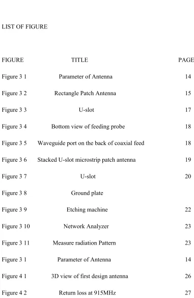
LIST OF FIGURE
[image:13.612.146.527.91.677.2]FIGURE TITLE PAGE Figure 3 1 Parameter of Antenna 14 Figure 3 2 Rectangle Patch Antenna 15 Figure 3 3 U-slot 17 Figure 3 4 Bottom view of feeding probe 18 Figure 3 5 Waveguide port on the back of coaxial feed 18 Figure 3 6 Stacked U-slot microstrip patch antenna 19 Figure 3 7 U-slot
Figure 3 8 Ground plate
20
xiii
[image:14.612.146.524.64.690.2]Figure 4 3 (a) 3D gain (b) Polar gain 28 Figure 4 4 (a) 3D Directivity (b) Polar Directivity 29 Figure 4 5 : S11 plot length of patch 30 Figure 4 6 S11 plot width of patch 31 Figure 4 7 S11 plot length of slot 31 Figure 4 8 S11 plot width of slot 32 Figure 4 9 3D view of design antenna 33 Figure 4 10 Return loss 34 Figure 4 11 (a) 3D Gain (b) Polar Gain 35 Figure 4 12 (a) 3D Directivity (b) Polar Directivity 36 Figure 4 13 Prototype stacked microstrip antenna 39 Figure 4 14 Received power for frequency 915MHz 39 Figure 4 15 Equipment for measure cable loss and power
receiver
40
Figure 4 16 S11 plot for measurement 41 Figure 4 17 E-H and E-E plane 42 Figure 4 18 H-E and H-H plane 42 Figure 4 19 S11 plot for simulation and measurement 43 Figure 4 20 Comparison between simulated results and
measurement results
xiv
ABBREVIATION
CST - Computer simulation technology
dB - Decibel
MHz - Megahertz
VSWR - Voltage standing wave ratio
RL - Return loss
SRD - Short Range Device
CHAPTER 1
INTRODCUTION
1.0 Project Briefing
For basic wireless communication system, it consists of a transfer medium, transmitter and receiver. The demand for small size, light weight and low cost antenna has increased with the widespread development of wireless communication like satellite communication. This project is about development high gain antenna for off grid wireless communication system. This project focus on high gain antenna to cover off grid wireless communication if the antenna cannot be used. It is the alternative wayto communicate to cover isolated area. The designing stacked antenna with frequency lass than 1GHz is design by using CST suite. Then the antenna will connected to short range device.
1 HEADING 3 – CHANGE COLOR TO WHITE BEFORE PRINTING
1.1 Problem Statement
2
Commission(MCMC) have presented recurrence range for Short Range Device (SRD) [3]. This useful when communication using a normal mobile phone without normal communication.
So, the antenna can be considered as the backbone to wireless system. Narrow band antenna are not suitable due to their limited bandwidth [4]. Microstrip antenna are extremely suitable for these application because they are compact and low profile while offering good performance. Compact microstrip antenna have recently received much attention due to the increasing demand of small antenna for personal communication equipment.
1.2 Objective
The main objective of this project is to develop high gain antenna for off grid wireless communication system. The objectives have been declared and must be achieved in completing this project. The objectives is a guideline of any project, thus the objectives of the project are :
i ) To design high gain antenna for off grid wireless communication system ii ) To design and simulate high gain antenna that suitable for SRD application (915MHz)
iii ) To simulate and analyze the proposed design through the simulation of high gain antenna using electromagnetic(EM) simulator such as CST.
Iv ) To evaluate and verify the design in laboratory and field test environment.
1.3 Scope
3
antenna design includes finding on the basic parameter such as resonant frequency, return loss, gain, directivity, and efficiency. The fabrication process is done by using chemical etching. This is because chemical etching technique is simple to be implemented and found in the faculty. The material used for designing the antenna is FR-4 board which has the specification such as dielectric constant of substrate, tangent loss of substrate, thickness of substrate and thickness of copper. The measurement will only be done after fabrication process. Antenna parameter such as resonance frequency, return loss, gain and directivity will be measured. After that, the field test was done with connected to the srd device to determine the distance that antenna can be transmit signal.
1.4 Organization of thesis
Chapter 1 will briefly discuss on the overview of the project carried out. The overview including the background of the project, problem statement, project motivation, project objective, scopes and limitations and outline will be presented in this chapter. This chapter will also explain the reason to design this antenna.
Chapter 2,this chapter has undertaken other projects to gain knowledge and information needed to complete this project. To make this project successful, information from primary sources for this project from a previous project and related thesis project are collected. Other sources such as book, journals, and articles obtained from internet. So this chapter discusses the project which related to the project.
Chapter 3 will explains the methodology of project in detail. Methodology is one of the important parts to the project. It is important to determine the methodology used to ensure the success of this project. Beside that to ensure that project meets the scope and reach goals of the objective
4
„transient solver‟ with default setting. Initially, simulation is performed using analytically computed antenna parameters.
5
CHAPTER 2
LITERATURE REVIEW
2 HEADING 3 – CHANGE COLOR TO WHITE BEFORE PRINTING
2.1 Introduction
This task has undertaken other projects after gain competencies or statistics wished in conformity with whole this project. To perform the project successful, information from previous project and related thesis project are collected. Other sources such as like book, journal, then article from internet. So, this chapter discusses the project which is related to the project.
2.2 Literature survey
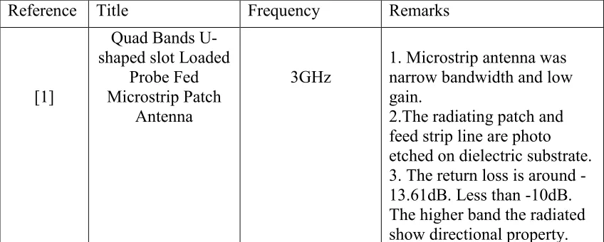
Literature survey was performed on a journal to collect related information and facts that can be used in the design process. It was carried out by performing a review of the literature in several journal related to the research. Table 1 summarise the sample of reviewed journal.
At the table, for reference microstrip patch antenna with the U-shaped Slot Loaded probe fed was presented[5]. U-slot patch antenna not only for wideband application, but it also can do for dual-band and triple band application. With the lower frequencies, the antenna acceptable gain that suitable for unidirectional and omnidirectional antenna application.
6
cubeSat depands on VHF/UHF with monopole and dipole antenna[6]. The return loss was around -10db at 2.46 and it was ideal. But it produce maximum gain of 9.6 dB at 2.4GHz. For tempered line, 50Ω coaxial feed is proposed as antenna input and placed at center to divide power equally.
The antenna designed is patch antenna for S-Band Application, such as WiMAX. [7] This antenna is circle in shape and also E-shaped. The circular patch gives larger gain and higher bandwidth whereas the E-shaped patch antenna is used to provide minimum return loss. It operates at 3.51 GHz with return loss at -19.6 dB, 9.13dB gain with 1.2 VSWR. Substrate used is FR-4, permittivity is 4.4.
On the other hand, the high gain filtering antenna was presented[8]. The high gain filtering antenna with 13.6% impedance bandwidth covering LTE band (2.3-2.7GHz). However, to shift from LTE band(2.3-2.7GHz) to WCDMA band(1.92-2.17GHz), the stacked patch and driven patch should to increase. The impedance bandwidth for 12.8% can make the gain bandwidth is narrower compare to the 20.7% of the impedance bandwidth. But, in filtering performance, it was same[8].
[image:22.612.108.532.483.653.2]
Table 1 Comparison of article
Reference Title Frequency Remarks
[1]
Quad Bands U-shaped slot Loaded
Probe Fed Microstrip Patch
Antenna
3GHz 1. Microstrip antenna was narrow bandwidth and low gain.
7
[2]
High Gain Patch Antenna for CubeSat
2.46 GHz
1. Design array cubeSat - increase gain and good impedance matching 2. Give gain 9.6dB. 3. provide low bit rate to provide high bit rate
[7] simulation of Patch Design and Antenna for 3.51GHz S-Band and WiMAX Apps
3.51 GHz
1. By circular patch - provide high gain and bandwidth
2. Add E-shape
- provide minimum return loss
3. Gain achieve 9.13 dB - combination of circular and E-shape
[8]
High Gain Filtering Antenna for
WCDMA Apps
2.3 GHz - 2.7 GHz
1. Add 3 radiation null - improve boresight high gain
2. Tune radiation null - effect the impedance bandwidth
8
[9]
High Gain
2.45GHz 2x2 Patch Array Stacked Antenna
2.45 GHz
1. Add air gap between radiating element and reflector
- increase bandwidth,gain 2. array element with chamfer edges
- improve the polarization capability
3. Achieve 19.29 dBi
[10]
High Gain Stacked Antenna Array for 60GHz
Communication System
60GHz
1. aperture coupler technique
- high gain and wide impedance bandwidth 2. Add array
- reduce mutual coupling 3. Achieve gain 18.09dB
[11]
Design of Stacked Segmented Ultra Wide Band Antenna
10GHz-19GHz
1. Increase the height of the stacked
- perform better frequency bandwidth