Rochester Institute of Technology
RIT Scholar Works
Theses
Thesis/Dissertation Collections
2003
Concept, design, simulation, and fabrication of an
ultra-scalable vertical MOSFET
Keith H. Tabakman
Follow this and additional works at:
http://scholarworks.rit.edu/theses
This Thesis is brought to you for free and open access by the Thesis/Dissertation Collections at RIT Scholar Works. It has been accepted for inclusion in Theses by an authorized administrator of RIT Scholar Works. For more information, please [email protected].
Recommended Citation
Concept, Design, Simulation, and Fabrication of an
Ultra-Scalable Vertical MOSFET
By
Keith Tabakman
Thesis submitted to the Faculty of
Rochester Institute of Technology
in partial fulfillment of the requirements for the degree of
Master of Science in Microelectronic Engineering
Approved By:
Chairperson: Dr. Sean L. Rommel
Sean
L.
Rommel
7{
)C(03
Santosh K. Kurinec
01-(2-6(03
Karl D. Hirschman
~b.~3
Committee: Dr. Santosh
K. Kurinec
Concept, Design, Simulation, and Fabrication of an
Ultra-Scalable Vertical MOSFET
I, Keith H. Tabakman, do hereby grant permission to the Wallace Memorial Library of
the Rochester Institute of Technology to reproduce my thesis in whole or in part without
my expressed written consent.
Signature of Author: _ _
K_e_it_h_H_e_T_a_b_a_k_m_a_n_
Table
ofContents
TableofContents hi
ListofFigures v
ListofTables vi
Abstract vii
Acknowledgments viii
Chapter 1: Introduction andMotivation 1
1.1 Vertical MOSFET Features 3
1.1.1 Vertical Channel 4
1.1.2
Epitaxy
41.1.3
Delta-Doping
51.2 Vertical MOSFET Benefits 6
1.2.1 Higher Speed 6
1.2.2 Lower Power 7
1.2.3 Higher
Density
81.2.4 Lower Cost 8
Chapter 1 References 10
Chapter 2: Prior Art 13
2.1 Device Metrics 13
2.1.1 OnandOffState Currents 13
2.1.2Subthreshold Characteristics 15
2.1.3 Drain Induced Barrier
Lowering
172.2Advanced Planar MOSFETs 18
2.2.1 Silicon On Insulator 19
2.2.2Strained Silicon 19
2.3 MultipleGate Ultra-thin
Body
Sidewall FETs 212.3.1 Double Gate Structures 22
2.3.2 Tri-Gate Structures 23
2.4 The Vertical MOSFET 23
2.4.1 Sidewall Vertical MOSFETs 24
2.4.2
Surrounding
Gate Transistors'.
24Chapter 2 References 26
Chapter 3: Device Design 31
3.1 Shallow Source / Drain Contact Regions 32
3.2 Source/Drain Extension 33
3.3Anti-Punchthrough
Delta-Doping
333.4 Channel
Doping
343.5Sii_xGex
363.6 Metal GateandAdvanced Gate Insulators 36
3.7MinimizationoftheMiller
Overlap
CapacitanceviaSelective Oxidation 37Chapter 4: Device Simulation 42
4.1 Introductionto Silvaco 42
4.2 Model Parameters 44
4.3 SimulationofAdvanced Devices 46
Chapter 4 References 49
Chapter 5: Device Fabrication 50
5.1 VMOSFET Fabrication Process 51
5.2 Process
Technology
Development 525.2.1 SidewallOxidation 52
5.2.2 Thermal Budget
Testing
615.2.3 PETEOS OxideCharacterization 65
Chapter 5 References 67
Chapter 6:Analysis ofResults 69
6.1 Calibration Sample
Testing
696.2 Thermal Ioff / Breakdown
Testing
726.3 Vertical MOSFET
Testing
746.4 AnalysisofMOSGated Tunnel Diodes 77
6.5 Wafer VariationandEffectsonMOSGTDs 80
Chapter 6 References 82
Chapter 7: ConclusionsandSuggestions 84
7.1 Vertical MOSFET 84
7.2 MOS Gated Tunnel Diode 85
List
ofFigures
Figure 1.1 Thefutureofsemiconductordevicespredicted
by
the2001 ITRS 3Figure 1.2Comparisonof a planarMOSFET 4
Figure 2.1 Typical DriveCurrentsvs. ChannelLength 14 Figure 2.2 Typical LeakageCurrentsvs.ChannelLength 14
Figure 2.3 Ion/Ioff Ratiovs. ChannelLength 14
Figure 2.4 TypicalSubthreshold Characteristicsvs. Channel Length 16
Figure 2.5 AnIllustrationofDIBL 17
Figure 2.6 Typical DIBLvs.Channel Length 18
Figure 2.7 SOI CMOS 19
Figure 2.8 Illustrationof aStrained Silicon MOSFET 20 Figure 2.9
Mobility
Enhancement for Strained Silicon MOSFETs 20 Figure 2.10 Cross Sectionsof aMultiple Gate Ultra-thinBody
Sidewall FETstructure.21Figure 2.11 Orientations ofDouble Gate Devices 22
Figure 2.12
Surrounding
Gate Transistor 25Figure 3.1 Schematiccomparison ofa planarMOSFETandtheproposed
VMOSstructure 32
Figure 3.2
Mobility
vs.Doping
35Figure 3.3 Gate Dielectric
Roadmap
2001 37Figure 4.1 Electric
Field,
including
cross sectionsatthesurface andinthebulk 46 Figure 4.2 Ids/ Vgs characteristicswithdifferentchannel dopings 47 Figure4.3 RITD structureandI-V Characteristics 47Figure5.1 Flatbandextraction 56
Figure 5.2 Critical fieldextraction 58
Figure 5.3 Cross Sectional SEMandEDXanalysis 59
Figure 5.4 Comparisonofoff state currents 63
Figure 5.5 Dielectric Field StrengthofPECVDOxide 66 Figure 6.1MOS
Family
ofCurves foraVertical MOSFET 74 Figure6.2 MOSFamily
ofCurves for Vertical MOSFETwithVg=0V Removed 75 Figure6.3 IncreasedVdd
Sweep
onVertical MOSFETDevice 76Figure6.4 Epitaxial Layers 76
Figure6.5
Energy
Diagramofthep-nJunctionat300KandNo Bias Voltage 77 Figure6.6Simplifiedenergy-banddiagramsoftunneldiodes 78 Figure 6.7DemonstrationofMOS Gated Tunnel Diodes 79Figure 6.8PVCRand
Ipeak
vs.Location 80Figure6.9 PVCRand
lpeak
vs.DeviceSize 81Figure 6. 10 PVCRvs. Gate Voltage 81
Figure 7.1 Anoptimized verticalMOSFET 85
List
ofTables
Table 2.1 ITRS Ion/Iff Requirements(2001
ITRS)
15Table 5.1 VMOSFET Fabrication Process 51
Table 5.2 ElectricalOxideThickness ofVertical Oxide 59
Table 5.3 Field Strength 61
Table 5.4Comparisonofthermalbudgettestspre andpostsinter 64
Table6.1 Calibration Sample Sheet Resistance Measurements 70
Table 6.2 Thermal
Testing
Abstract
Anew orientation to the conventional MOSFET is proposed.
Processing issues,
as well as short channel effects have been makingplanar MOSFET scaling
increasingly
difficult. It is predicted
by
the 2001 InternationalTechnology Roadmap
for Semiconductors(ITRS)
thatnon-planardeviceswill beneededforproductionas earlyas2007. The device proposedin this thesisis similar inoperationto theplanar
MOSFET,
however the current transport from source todrain,
normally in the same plane as thewafer surface, is oriented perpendicular to the die surface. The proposed device has successfully been simulated, showing a proofof concept. Fabrication ofthe proposed devices led to the creation ofvertical MOS Gated Tunnel Diodes. This work, in
fact,
represents possiblythe first demonstration ofthis type oftechnology. Suggestions are
Acknowledgments
I would like to express mysincere thanks and gratitude to the manypeople who
have contributedto thiswork.
Dr. Sean L.
Rommel,
for offering his advice and guidance. His serving as mythesisadvisor madethis project,andthesubsequent results possible.
Dr. Santosh K.
Kurinec,
for serving as one of my thesis committee members. Dr. Kurinec has gone above andbeyondthecall ofduty
toaid mein mytimehereatRIT.Dr. Karl D.
Hirschman,
for serving as one of my thesis committee members. Dr.Hirschman's energy and knowledgehas promoted an excellent working environment at
RIT.
Dr. Phil E. Thompson
(USNRL),
forproviding hisservices andinputfueling
thisproject.
Branislav
Curanovic,
StephenSudirgo,
andRohitNandgaonkar,
fortheirsupportinfabricationas wellas
during
testing.Charles
Gruener,
for hissupportbothwithsimulations andmaskcreation.The RIT Microelectronics
Faculty
andStaff,
theirassistance andfriendship
overtheChapter 1
INTRODUCTION AND MOTIVATION
The fuel ofthe integratedelectronics
industry
is the transistor. In1965,
GordonE. Moore (Intel
Corp.),
made his famous prediction that the number oftransistors persquare inch on an integrated circuit would double every 18 months [1]. The scaling of
thetransistors in integrated circuits allows for fourmajorimprovements
(i)
higher speed(ii)
lowerpower(iii)
higherdensity
and(iv)
lower cost. In all ofmanufacturinghistory,
no other product has exhibited the characteristics ofthe
transistor,
in which the speedincreases andthe cost of production decreases as the size is reduced [2]. Over the past
twenty
years, thespeed ofthetransistorhas increased 20 times andthesize has shrunktooccupy lessthat 1%oftheareaoriginallyrequired.
By demonstrating
smaller and faster devices the world has becomehungry
formore performance andintegration. This has acceleratedthescalingtrendsof
lithography,
the effective channel length
(Leff),
the gate dielectric thickness(tox),
supply voltage,device
leakage,
etc [3].Many
innovations have gone into extending the life of theMOSFET such as the use ofstrained silicon
[4],
silicon on oxide[5],
and pocket/ halosome point, the physical challenges that impede the transistor's progress will overcome
the research thrusts powering Moore's law. These challenges take the form ofprocess
related as well as physics relatedissues.
The International
Technology Roadmap
for Semiconductors(ITRS)
[3],
developed
by
International SEMATECH in communications with the SemiconductorIndustry
Association(SIA),
the European Electronic Component Association(EECA),
the Japan Electronics and Information
Technology
Industries Association(JEITA),
theKorean Semiconductor
Industry
Association(KSIA),
and Taiwan SemiconductorIndustry
Association(TSIA),
predicts the future ofthe integrated circuit industry. Theroadmap outlines the needs of future process technologies in order to realize the
aggressivescaling defined
by
Moore'slaw.The long-term challenges identified in the 2001 ITRS roadmap are control of
criticaldimensions aswell as
Leff,
high-kmaterialsas gateinsulatorsduetotheextremelythinnatureofthese
films,
the thermalstabilityofthesehigh-kfilms,
andtheuse ofmetalgatesjustto name a few. These issues are currently inresearch, howevernoneof which
has an answerreadyto moveto themanufacturing sector. These
technologies,
however,
areprojectedtobe ready (ornecessary)
by
2006-7 [3].Additionally
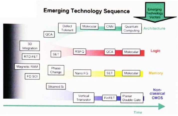
the roadmap identifies future technologies that may eventuallyovercome the planar transistor in order to prolong the effectiveness of Moore's law
(figure 1.1).
Many
methods for achieving the process technologies needed for futureEmerging Technology
SequenceToturnnl
Mil.<
i -1/ CNN
Ptvaw; CtisnQfl
St/atnad St
VLMttCdl Transtslor
Quantum Comfxjting
Motocuiar
Tocfuiolotjy Man
!_ Double Gate I Logic
Memory
Non-classical
CMOS
Time
Figure1.1: Thefutureof semiconductordevicespredictedbythe2001 ITRS
Strained
Si,
in which the active area silicon is stretchedincreasing
carriermobility, is already
being
used in the most advanced production integrated circuits.Strained Siis describedin Chapter 2 inmore detail. Muchworkhas showntheimproved
scalabilityofthefinFET
[8-10], however,
thefinFET device isstilllimitedby
theprocesstechnologies currentlyunderquestion
by
the ITRS. The use oftheextremelythinfins ofthefinFET raises some concern with series resistances. In addition,thegatelengthofthe
finFET is still ultimatelydefined
by lithography
andetchingtechniques,
andis subjecttoprocess variations [11]. Some work has recently been presented on the Vertical
Transistor
(VMOSFET),
this device similarly exhibits improved scalability over theplanarMOSFET.
However,
the VMOSFET does benefit from relaxed requirements of [image:12.527.123.480.39.271.2]1.1
Vertical MOSFET Features
The Vertical MOSFET proposed in this study features three major points
(i)
thechannel is oriented perpendicular to the plane ofthe starting substrate,
(ii)
the device iscreated almost whollythrough the process ofepitaxy, and
(iii) delta-doping
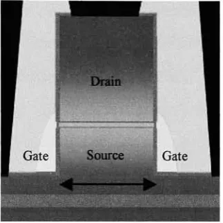
planes exist between each source/ drain andthe channel. Figure 1.2 compares a planarMOSFET totheproposedVertical MOSFET device.
/Source . v; . ' ; Drain
f . Source/Dram . V Fxtftnsinns F""'
-Antipunchthrough
(a) (b)
Figure1.2: Comparisonof a planarMOSFET(a)andtheproposedVertical MOSFET(b)
1.1.1
Vertical Channel
The channel region of the proposed Vertical MOSFET is oriented such that the
direction of current flow is perpendicularto the surface ofthe starting substrate.
Using
advanced
lithography
and etching techniques then, afully
depleted structure may bemade ina similar methodto finFETs
[8,10,13]
or SOI MOSFETs [10].It is observed that the channel region exists completely above the surface ofthe
substrate. The channel region is completely surrounded
by
the gate. Since the channeldoes not reside in the bulk the device is essentially built in an SOI fashion. Due to the
fully
surrounding nature of the gate, the gate acts to shield the device making it1.1.2
Epitaxy
Molecular Beam
Epitaxy (MBE)
is used to define the devicedoping
profiles.MBE is capable ofgrowing atomic thickness films. Because ofthis the
doping
profilescan be controlled extremely well. Junctions may be made very abrupt, and the use of
MBE allows forthe use of
delta-doping
[14]. Thedoping
ofthe channel region may betailored to alterthe electric fieldproperties withinthe channel, aidingcarriertransportin
thedesired direction.
1.1.3
Delta-Doping
It is our hypothesis that this layer is essential to the scalability of the vertical
MOSFET device. The delta-dopedlayeris doped atasignificantly higherconcentration
then the source anddrainregions. Because ofthisthe6-doped layers effectivelybalances
the charges between thechannel and source ordrainwithin adepletionregion extending
intothesourceordrainand
terminating
atthe5-doping
plane.Thecontrolofthedepletionregions acts similarto thatofpocket,orhalo implants
in today's planar CMOS devices. Since the delta-doped region exists everywhere
between the source / drain and the channel, the possibility ofpunch-through is almost
eliminated.
Straddling
the 5-dopedplaneareverythin layers ofSiGe. It has been shownthatdiffusion ofp-type dopants is retarded in thepresence ofGe [15]. This aids in
keeping
the 6*
-doping plane extremely
thin,
increasing
the probability oftunneling,
as the 51
.2Vertical MOSFET
Benefits
1.2.1
Higher
Speed
In the on state, a majority carrier from a MOSFET's source terminal is injected
into the channel region. Due to interactions with the crystalline structure of the
semiconductor, a collision, or scattering event is statistically inevitable. The statistical
mean ofthe time it takes for a carrier to experience a scattering event is known as the
mean free time. Asimilar explanation can be givento themean free path.
Using
thesetwo statistical pieces ofinformationonemay determineamaximumvelocityat whichthe
average carriermaymovethroughout thesemiconductor. A
long
channel transistorin itsnormal onstate, isgenerally inthesaturation region ofoperation. Inthis region, carriers
withinthechannel move withthesaturation velocity.
It is obvious then, that
by decreasing
the distance between the source and thedrain of a MOSFET
device,
the time it takes for a carrier to travel this distance isdecreased. This inturnincreasesthespeedofthedevice.
The probabilityof acollisionis proportionalto the electric field inthechannelof
thetransistor,
increasing
towards the drainofthe device. The fieldstrength increases asthe channel lengthofthe transistors decreases. These collisions can create electron-hole
pairs. The created electrons can be injected into the gate oxide
degrading
its qualitywhile the hole may be swept into the bulk creating a potential
drop
in thebulk,
whichmaylead tosnapback.
By
controllingthe depletionregions withinthe channel, thespeedofthe Vertical MOSFETbenefits inthree ways:
(1) by
limiting
the depletionwidthintothe channel, the source and drain may be brought closer together without fears of short
the channel,hotcarrier effects are less
likely; (3)
the chargebalance occursbetweenthedelta-dopedregions andthesource/drainsallowing forreducedchanneldoping.
1.2.2
Lower Power
Associatedwiththedecreased length oftheMOSFET channelis adecrease in the
powersupplyvoltage. This is doneto maintain a constantfieldinthedevice throughout
the scaling process. While the decrease in power helps in controlling short channel
effects created
by
high fields within thedevice,
a certain potential range must bemaintainedinordertoextendtheusabilityofthesmalltransistorin integratedcircuits.
A significant portion of the total power used
by
a chip is the standby powerassociated with transistors not
being
used. This standby power becomes even moresignificant as leakage currents increase with decreased device dimensions. It is very
important,
then, to minimizethisleakage current,morecommonly knownastheoffstatecurrentor Ioff.
Ioff
occurs dueto drift anddiffusionwithin theMOSFETs junctions. Theuse ofepitaxy to define the source, channel, and drain ofthe vertical MOSFET limits
some ofthis leakage current,
by
creating extremely abruptjunctions with little damage.Damageassociated with
high-energy
particles, such asthosefound inplasmas,have beenshowntocreate defectsthatincrease leakagecurrents [16]. Ifthedamage induced
by
theion implantation process is not properly annealed out, it will cause excessive leakage
current. The vertical MOSFET device is essentially built
by
epitaxy. Defects can bepresent in epitaxially grown
layers,
however thedensity
of the majority defects issignificantlyreduced ifthe process temperature is kept above 600C [17].
By
using theIt ispredictedthat theuse of
delta-doping
planeswillassistinminimizing leakagecurrent.
1.2.2 Higher
Density
The vertical MOSFET leads to a significant
jump
in the achievabledensity
ofintegratedcircuits [3].
By
aligningthedevicesuch thatthedrain isdirectly
ontop
ofthesource, the real estate taken up
by
these regions will decrease. Various methods havebeen
identified,
ofstackingtheverticaldevices inorderto createmultipletransistorgateswiththefootprintof one suchtransistor.
1.2.3 Lower Cost
No advanceddevice can be consideredfor manufacturing before it canbe shown
that the cost ofproducing integrated circuits would be no more expensive, ifnot less
expensive ofthose
being
created today.Taking
into account theincreasing
number ofinterconnectlevels inthebackend processing ofmodern
IC's,
thebackend accountsforasignificant portion of fabrication costs. Since the fabrication details of the vertical
MOSFET device proposed in this study includes no ion implant steps, a decreased
number ofmasking
levels,
anda lowerthermalbudget,
the costofproducing IC's usingtheverticalMOSFETprocess willbe lessthan thatoftheIC's
being
producedtoday.It should be noted that in the past the epitaxy process has been considered a
lengthy
andexpensive process. The major disadvantage for epitaxy isthroughput,
as itisoften a single-wafer at a time process. Single wafer systems,
however,
have beenoptimized to the point that
they
not only approach, but in some cases exceed batchdue to decreased junction depths. The
tightening
ofspecifications has reachedthepointat which epitaxial substrates are required. The profitability of polished waferproducts
has been
deteriorating
while the margins in epitaxial wafer preparation remain decent[1]
G. E.Moore,
"Cramming
More Components Onto Integrated Circuits,"Electronics
Magazine,
Vol.38,
No.8,
April19,
1965.[2]
R.D.Isaac,
"Reaching
the Limits of CMOS Technology," IEEE 7th topicalMeeting
onElectrical PerformanceofElectronicPackaging,
1998. Pg. 26-28.[3]
"The InternationalTechnology Roadmap
forSemiconductors",
Publishedby
theSemiconductorIndustrial
Association,
SanJose,
CA.[4]
XinWang; Kencke, D.L.; Liu, K.C.; Tasch, A.F., Jr; Register, L.F.; Banerjee,
S.K.;
"Electron transport properties in novel orthorhombically-strained siliconmaterial explored
by
the Monte Carlo method,"Simulation of Semiconductor
Processes and
Devices,
2000. SISPAD 2000. 2000 International Conference on ,6-8 Sept.
2000,
Page(s): 70-73.[5]
Cristoloveanu, S.;
"Silicon on insulatortechnology,
devices,
andchallenges,"
Optoelectronic and Microelectronic Materials
Devices,
1998. Proceedings. 1998Conferenceon, 14-16 Dec.
1998,
Page(s): 44-48.[6]
BinYu; Wann, C.H.J.; Nowak, E.D.; Noda, K;
Chenming
Hu;
"Short-channeleffect improved
by
lateral channel-engineering in deep-submicronmeterMOSFET's,"
Electron
Devices,
IEEE Transactions on , Volume: 44 Issue: 4 ,April
1997,
Page(s): 627-634.[7]
Das, A.; De, H; Misra, V.; Venkatesan, S.; Veeraraghavan, S.; Foisy, M.;
"Effects of halo implant on hot carrier reliability of sub-quarter micron
MOSFETs,"
Reliability
Physics SymposiumProceedings,
1998. 36th Annual.[8]
BinYu;
LelandChang; Ahmed,
S.;
Haihong
Wang; Bell, S.;
Chih-YuhYang;
Tabery, C;
ChauHo;
QiXiang;
Tsu-JaeKing; Bokor, J.;
Chenming
Hu;
Ming-Ren
Lin;
Kyser,
D. "FinFET scaling to 10 nm gatelength"
Electron Devices
Meeting,
2002. IEDM '02. Digest. International ,8-11 Dec.2002,
Page(s): 251 -254.[9]
LelandChang;
Yang-KyuChoi; Kedzierski, J.; Lindert, N;
PeiqiXuan;
Bokor, J.;
Chenming
Hu;
Tsu-JaeKing
, "Moore's law lives on [CMOStransistors]"
Circuits andDevices
Magazine,
IEEE , Volume: 19 Issue: 1 , Jan.2003,
Page(s):35-42.
[10]
Hisamoto, D.;
Wen-ChinLee;
Kedzierski, J.; Takeuchi, H.; Asano, K; Kuo, C;
Anderson, E.;
Tsu-JaeKing; Bokor, J.;
Chenming
Hu,
"FinFET-a self-aligneddouble-gate MOSFET scalable to 20 nm,"
Electron
Devices,
IEEE Transactionson,Volume: 47 Issue: 12 ,Dec.
2000,
Page(s): 2320-2325.[1
1]
Y.-K.Choi,
N.Lindert,
P.Xuan,
S.Tang,
D.Ha,
E.nderson,T.-J.King,
J.Bokor,
andC.
Hu,
"FinFET ProcessTechnology
for NanoscaleCMOS,"
IEDM Tech.
Digest,
p.421(2001).[12]
D.J. Franketal.,"DeviceScaling
Limits ofSi MOSFETSandTheir ApplicationDependencies."
Proceedings ofthe
IEEE,
Vol.89,
No.3,
March 2001.[13]
H.-S.PWong,
"BeyondtheConventionalTransistor"IBMJRD,
V.46,
N.2/3,
2002.
[14]
GossmanH.-J., Schubert,
E.F.,
"DeltaDoping
in Silicon," Critical Reviews in[15]
Li,
H. -J,Kirichenko,
T.A., Kohli, P., Banerjee,
S.K, Graetz, E., Tichy, R,
Zeitzoff,
P.,
"Boron Retarded Diffusion in the Presence of Indium orGermanium,"
IEEE Electron Device
Letters,
Vol.23,
No.11, November,
2002.Page(s): 646-648.
[16]
Balasinski,
A.;
Petti,
C;
Bamnolker,
H;
Ramkumar,
K;
Chung,
A.,
"Characterization of plasma induced damage using transient current
measurements,"
Plasma Process-Induced
Damage,
1998 3rd InternationalSymposiumon, 4-5 June
1998,
Page(s): 26-29.[17]
Chung,
S. -Y,Jin, N, Rice,
A.T., Berger,
P.R, Yu, R, Fang,
Z. -Q.,Thompson,
P.E.,
"Growth Temperature and Dopant Species Effects onDeep
Levels in Si Grown
by
Low Temperature Molecular Beam Epitaxy," Journal ofApplied
Physics,
Vol.93,
No.11,
June2003,
Page(s): 9104-9110.[18]
Royalty,
R. "Silicon Epitaxy: Tomorrow's Solution Today,"Semiconductor
FabTech,
Ed.15,
Dec. 2001.[19]
Semi,
"Epitaxy
has Potential to Become the Lowest Cost ICStarting
Material,"Chapter 2
BACKGROUND
As the need for smaller,
faster,
and cheaper devices speeds up, the need foradvanced device structures becomes more and more evident.
Many
advanced deviceshave beenproposed and explored. The three majorcompetingtechnologies are those of
advancedplanar
MOSFETs,
Multiple Gate Ultra-thinBody
SidewallFETs,
andVerticalMOSFETs. In this chapter, each devicewillbe
discussed,
alongwithprocessing detailsand resulting electrical characteristics. It is
important,
in comparison, to discusscompeting device technologies in terms of the metrics involved in characterizing the
devices.
2.1
Device Metrics
2.1.1
On
andOff State Currents
According
to the 2001 ITRS[18,19],
the device metric CV/I can be used toestimate device switching speed. The metric can be derived from intrinsic device
capacitances, the voltage swing necessary to drive a
following
stage, and the driveindependent ofdevice size. From this definition it can be determined that drive or
on-state current in a device is an important metric when attempting to design fast devices.
Often the on state current for a device is reported at a constant off state or standby
current.
Iaavs.Channel length I vs.Channellength
1.3
| | i ]
j i
j i j 1 1 :
[12-IBM] ."[4 -Intel] 1.0 0.9 0.6 (3 -rntelj
(11-Fujitsu) (6-Samsung]
0.6 [13-AMD] ',.Inte,,
r [16-AMD] -L__ H5 [14 -Intel] UCBerkeley] : I : Planar ! finFET ^ --Vertical [5 -BellLabs] 0.0 [9 -SiemensAG]
i . i . i . i i
-0.1
20 30 40 50 60 Channel Length(nm]
120 110 100 90 80 70 60 50 40 30 20 10 0 -10 -20 -30
I ' I 1
:
[14-Intel]W -Fujitsu] j-
1
[6 -Samsung] j [image:23.527.65.472.161.338.2] [image:23.527.171.366.398.566.2]"[15-UCEerkeey] *[* -Intel]
[13-AMD]
j
T10-AMD7!motorola]
'
-[9-SiemensAG] i
f3-Intell'
_
Planar finFET ? Vertical
[5-Bell Labs|
:
| ;
20 30 40 50 60 70
Channel Length[nm]
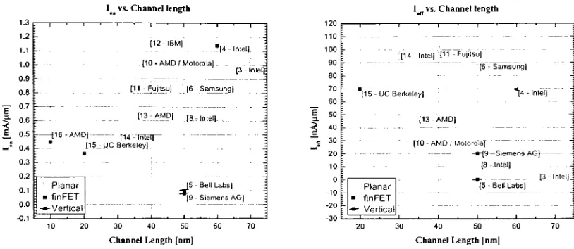
Figure 2.1: Typical Drive Currentsvs.Channel Figure 2.2: Typical Leakage Currentsvs.Channel
Length Length 1x10 1x10⁵ 9x10' 8x10' 7x10' 6x10' 5x10' 4x10' 3x10' 2x10' 1x10' 0 ; I
' I i l ' i ' l ' i
-Planar nnFET - Vertical [3 -Intel]: : - -[8 -Intel] : : ;
[10-AMD /
Motorola]
:
; ;
H
[13-AMD1 ',, , , 111-Fujitsu) "[4-Intel] 5-UCBerkeley] -- [6-Samsung] _
'
. r'-lnWl
(12 IBM]T[9-SiemensAG] j :
30 40 50 60 70
ChannelLength[nm]
Figure2.3: Ion/ Ioff Ratiovs.Channel Length
Figures 2.1 and 2.2 show some typical on and off state currents with respect to
as an average value, and assuming that 1/3 ofthe transistors on an integrated circuit are
on, and that the ICcontains amillion
transistors,
the leakagecurrent dueto transistors instandby mode would be 33mA. 33mA is not a large leakage current, but considering
today's integrated circuits are approaching 1 billion transistors, the standbycurrentusing
the same parameters would be 33 Amps! It is easy to see, then, that it is important to
keep
the off state current low. Table 2.1 illustrates the 2001 ITRS requirements forU
and
Ioff
parameters through 2016[18]
where'MPU'
stands for Microprocessor
Unit,
'LOP'
stands for Low
Operating
Power,
and'LSTP'
stands for Low
Standby
Power.lon[[iA/luti]
Year 1999 2000 2001 2002 2003 2004 2005 2006 2007 2010 2013 2016
MPU 1041 1022 926 959 967 954 924 960 1091 1250 1492 1507
LOP 636 591 600 600 600 600 600 600 700 700 800 900
LSTP 300 300 300 300 400 400 400 400 500 500 600 800
loff[[jA/|xm]
Year 1999 2000 2001 2002 2003 2004 2005 2006 2007 2010 2013 2016
MPU 0 . 0.01 0.01 0.03 0.07 0.1 0.3 0.7 1 3 7 10
LOP 1.0E-04 1.0E-04 1.0E-04 1.0E-04 1.0E-04 3.0E-04 3.0E-04 3.0E-04 7.0E-04 1.0E-03 3.0E-03 1.0E-02
LSTP 1.0E-06 1.0E-06 1.0E-06 1.0E-06 1.0E-06 1.0E-06 1.0E-06 1.0E-06 1.0E-06 3.0E-06 7.0E-06 1.0E-05
Table 2.1: ITRS Ion/Toff Requirements (2001ITRS)
Atransistor, in thedigital sense is essentiallya switch. In order forthe switchto
be effective the ratio between on state current and off state current must be
large,
otherwise there would be no way to reliablychain millions oftransistors together while
consideringthenoise margins associated witheach gate.
2.1.2
Subthreshold CharacteristicsAs mentionedabove,therange of oncurrentto offcurrentis importantin modern
subthreshold slope is defined
by
equation 2.1. The subthreshold slope is considered toindicatehowwellatransistorturns off.
S=
5(logio^)
v-ldV
( 1+ cdm C Equation 2.1 oxJIn equation
2.1,
Cdm
is the depletion layer capacitance [19]. The subthresholdslope is reported in terms of mV per decade of current. The theoretical limit of
subthreshold slopeis
kT/q
orthe thermalenergyofcarriers, howevertypicalvaluesofthesubthreshold slope are between 70 to 100 mV/decade. Figure 2.4 show typical
subthresholdcharacteristicsforcurrent researchdevices vs.theirchannellengths.
Subthreshold Slopevs.Channel length
5 100 >
' I ' I ' I ' I ' I '
"[16-AMD] Planar finFET ' --Vertical. [12-IBM] 15 -BellLabs] [14-Intel) ~J
[15
[13-AMD]
[1-UT
Austin] m -[2 -IBM] .i.i,
lp
-UCLA-UC Berkeley] [4-(8 -Intel] ill ntel] i .i.i.
0 10 20 30 40 50 60 70 80 90 100 110 120 130 Channel Length|nm|
Figure 2.4: Typical Subthreshold Characteristicsvs.Channel Length
In order to control subthreshold characteristics, the insulator separating the gate
from the channel of MOSFETs has decreased to thicknesses on the order of a few
2.1.3 Drain Induced Barrier
Lowering
Drain Induced Barrier
Lowering (DIBL)
describes the effect the drain potentialhas on the threshold voltage of a transistor. As a reverse bias is applied to one p-n
junction afield pattern is created that can lowerpotentialbarriers separatingthejunction
from an adjacent junction. If this
lowering
of the barrier is significant enough theadjacentjunctionbehaves as a source ofcarriers, resulting inundesirablecurrent.
Xisr
Cbff/E B YDS
URVE
-""
\L=I Z'-"'m\
Xos'5v
\ \
URVS
a-\
\
[image:26.527.179.371.214.356.2]01 02 05 CI 05 06 07 08 09
Figure 2.5: AnIllustrationofDIBL(figureadaptedfrom[20])
In order to control the barrier
lowering
in moderndevices,
channeldoping
hasincreased significantly. The use of super-steep retrograde wells
(SSRW),
and halo orimplants,
performed to placehighly
doped,
channel-type, regionsimmediately
below the source/drain extensions helps limit DIBL. Figure 2.6 illustrates typical DLBL
DIBLvs.Channellength > -J -5 110 100 90 80 70 60 50 40 30 20 10 0
. ' 1 ' 1 .
i .
i .
i . , . i . i
[14 -Intel] ]3-Intel]:
' I '
i
-(15-UCBerkeley)
: ; "(5 -Bell Labs] ;
i
._.. [16-AMD] | ':i
i[4-Intel] " |8 -Intel] '[2 -IBM] 1 ; - '
[1-UT
Austin]: : Planar
I finFET
-*
Vertical
-i i i i . i . i . i . i . i . i . ,
-0 10 20 30 40 50 60 70 80 90 100 110 120 130
ChannelLength[nm]
Figure 2.6: Typical DIBLvs. Channel Length
2.2
Advanced Planar MOSFETs
The original design foraplanarMOSFET requiredvery few
doping
steps,solid-source diffusion or implant. The device featured two similar-type diffused regions
separated
by
an alternate type channel region. A metal gate was placed above a thininsulator.
However,
as device dimensions shrunkthe need foradjustments to the devicearose. For example, in order to integrate devices a controlled threshold voltage is
required. In order to accomplish this, additional implants must be preformed in the
channel region
during
device fabrication. Similar additions such as retrograde wellimplants,
source/drain extensions, silicidation, and isolation have been added to thefabrication process. The channel lengthoftheplanar device is limitedto the availability
However,
all ofthese additions still cannot completely control the short channeleffects that dominate device characteristics of
deep
submicron and nanoscale devices.Becauseofthismore advancementshavebeenproposedtotheplanarMOSFET.
2.2.1
Silicon On Insulator
Devices built on a thin layer of crystalline silicon above an insulator were first
reported in the 1960's in order to produce devices that were
fast,
low power, and wellisolated [23]. The deviceswerebuilton silicon-on-sapphire substrates.
Currently
SilicononInsulator
(SOI)
substrates feature athindeviceregion separated from bulksiliconby
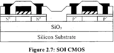
asilicondioxide layer. Figure 2.7 illustrates CMOS builton anSOIsubstrate.
N*
SiO,
[image:28.527.165.363.316.409.2]Silicon Substrate
Figure 2.7:SOI CMOS
Because ofthe complete isolation of
devices,
latch-up
is prevented. Since wellsare not needed for device isolation higher circuit densities can be achieved. In addition
since the source and drain junctions extend to the buried oxide
(BOX)
the capacitancesassociated with those junctions are significantly reduced. Because ofthis the devices
mayoperate fasterwhile
dissipating
less static anddynamic power. The junction areaofthe drain/channeljunction is limited. As a result, short channel effects associated with
the chargesharingbetweenthe gate andthedrainare reduced.
Similarly
thesubthreshold2.2.2 Strained Silicon
As mentioned earlier in this chapter, the on state current is
inversely
proportionaltodevicespeed. The mobilityof carriers is
directly
proportional to thesaturation current.Hence,
anyimprovement incarrier mobilitywillresult in faster devices.By
using alayerofa
Sii_xGex
alloy, the lattice of active region silicon is stretchedby
about one percent.The SiGe layer is grown thick enough to relax. The silicon lattice on
top
ofthis layerthen adopts the lattice constant of
SiGe,
solong
as the silicon layer is below a criticalthickness. This increase in lattice spacingreduces scattering,resulting in a3Xincrease in
mobility. Astrained siliconMOSFETis illustrated in figure 2.8.
B
Si iVSilicon GermaniumLayer
[image:29.527.172.364.307.367.2]Silicon Substrate
Figure 2.8: Illustrationof aStrained Silicon MOSFET
Figure 2.9 illustrates carrier mobility improvements due to different mole fractions of
germanium.
2.0r
_ 1.0
0.80
'' Walser IEDM '92
Walser IEDM '94
= Rim.VlSI'01 Calc forsl/ancdSi * Currie.2001[14]
(phonon-limited) 0 Teajka,VLSI'02 I
J
0.0 0.10 0.20 0.30
SubstrateGefraction,x
[image:29.527.166.358.480.646.2]0.40
Strainedsilicon andSOI have beenincorporatedto produceplanartransistors on a
Silicon Germanium onInsulator
(SGOI)
platform. Thatis,
planartransistors that featurebothstrained silicon as well asthebenefitsofaburied insulator.
2.3
Multiple Gate
Ultra-thin
Body
Sidewall FETs
The benefit of an ultra thin
body
SOI planar MOSFET is that the subthresholdcharacteristics are superiorto that ofbulkplanartransistors. Howeverinorderto createa
fully
depleted SOI MOSFET thetop
silicon thickness must be sufficientlythin to allowdepletion with small applied biases (e.g. < lOOnm). The Multiple Gate Ultra-thin
Body
Sidewall FETstructure alleviates some ofthis concern. A Multiple GateUltra-thin
Body
Sidewall FET features a thin fin of silicon over which a gate is placed. The Multiple
Gate Ultra-thin
Body
Sidewall FET can be of a double-gate or a Tri-gate configuration,meaning that the device depletes and inverts from either two or three sides. A cross
sections of aMultiple Gate Ultra-thin
Body
Sidewall FETis depicted in figure 2.10.Sifin
Source/ Drain^
BOX
Silicon Substrate
Silicon r'fm
BOX
Silicon
Figure 2.10: Cross SectionsofaMultipleGate Ultra-thinBodySidewall FETstructure
The Multiple Gate Ultra-thin
Body
Sidewall FET is a proposed replacement fortheplanar
MOSFET,
however similarto it'splanarcounterpart, thechannelofthe deviceand etch-backtechniques. Becauseofthe
fully
depleting
natureof a Multiple GateUltra-thin
Body
Sidewall FET itexhibits excellent electrostaticscalingproperties [22].2.3.1
Double Gate
Structures
Adouble gate structure depletes from two sides ofthe silicon fin. The transistor
widththenis double thefin height. When
fabricating
adouble gateMultiple GateUltra-thin
Body
SidewallFET,
a hardmask is usedto define the silicon fin. This hard maskmayeitherbesilicon
dioxide,
nitride, oranyotherinsulating
etch-resistant material. Thishard mask is then left in place
during
gate oxidation, and subsequent gate materialdeposition [4,15].
Since the gate resides on either side of the
device,
during
turn-on the channelregion depletes from either side of the silicon
fin,
allowing the existence of afully
depleted device with somewhat relaxed fin width requirements. Because of this the
Multiple Gate Ultra-thin
Body
Sidewall FET has demonstrated some of the bestsubthreshold parameters ofany field effect transistor; such as a subthreshold slope of
68mV/decade fora40nmchannellength device [4].
It should be pointed out that the double gate FET does not necessarily have to
take the form of a Multiple Gate Ultra-thin
Body
Sidewall FET. The double gatetransistormay beorientedinthreebasicdirections (figure
2.11)
2.3.2 Tri-Gate Structures
Recently
Multiple Gate Ultra-thinBody
Sidewall FET structures weredevelopedwith even more relaxed fin width requirements [4]. The hard-mask used to etch the silicon finwas removed priortogate oxidation and gatedeposition. Thiscreated adevice
that depleted from three sides. While the double gate Multiple Gate Ultra-thin
Body
Sidewall FET has limited fin width, the tri-gateMultiple Gate Ultra-thin
Body
SidewallFETrequires
dimensionally
similarfin heightandwidthtomaintainthefull depletion.The tri-gate Multiple Gate Ultra-thin
Body
Sidewall FET demonstratedby [4]
demonstrates some of the best subthreshold parameters compared to planar 65nm
transistors. The subthreshold slope matchedthat ofthedoublegate MultipleGate
Ultra-thin
Body
Sidewall FETat 68 mV/decade. HowevertheDIBLparameter is very lowat41 mV/V. This speaksverywellforthisorientationoftheMultipleGate Ultra-thin
Body
Sidewall FET since as transistors scale smaller it is the off state that seems to be the
killer.
2.4
The Vertical MOSFET
Ever since epitaxy was introduced the concept ofcreating a MOSFET structure
featuring
current flowperpendicular to the substrate has existed. Dueto themethods of epitaxy, dopants can be verywell controlled.Doping
profiles can be tailored such thatchargedistributions and electricfields may becontrolled. Thiswas demonstrated
by
[1],
using epitaxyto grade the channel
doping
in a vertical MOSFET. The DIBLparameterforthe device demonstrated in
[1]
is 30 mV/V. Thesubthreshold slope ofthese devicesPlanar SOI MOSFETs benefit from the increased isolation associated with the
surrounding insulator. Vertical MOSFETs are almost always mesa
isolated,
which issimilar to the SOI concept. In mesa isolation islands ofdevice material are etched, the
channel ofthese vertical MOSFETs isthen onthe sidewall ofthesilicon pillar ormesa.
The inner layer dielectric separatingthe front-end fromthe backendthen isolates device
fromdevice. In bulk silicon, onlythesource/drain atthebottomoftheverticalMOSFET
then wouldbe common across an integratedcircuit. Ifthese devices were fabricatedon
SOIsubstratesthedeviceswouldbecompletely isolated.
Thereare multipletypesof verticalMOSFETs.
2.4.1
Sidewall
Vertical MOSFETs
Epitaxialsiliconmay begrown on
top
ofimplantedislands,
ortheepitaxiallayersmay be doped in-situ. Sidewall vertical MOSFETs are mesa defined before gate
oxidation. A contact to the bottom source/drain is then deposited on one side ofthe
device,
whilethegate is depositedanddefinedontheother side [9].Only
one side ofthedevice,
then, is usedas thetransistor. The integrationofthistypeoftransistoris farmorestraightforwardthen thatof
fully
surroundinggatetransistors.2.4.2
Surrounding
Gate Transistors
If the channel region of the epitaxially grown silicon mesa is completely
surrounded
by
the gate, the vertical MOSFET is considered an SGT or surrounded gatetransistor [1,5,7]. The surrounding nature ofthe gate, coupled with avery thin silicon
associated with a gate, the
surrounding
gate transistor exhibits the best electrostaticscalingproperties
[22].
Subsequently
since the gate completely envelopes thechannel region, the deviceis quite resilient inthe presence of radiation[24]. This is becausethe gate actstoshield
the channel of the
device
similar to a coaxial cable. Figure 2.12 illustrates afully
surroundinggate verticalMOSFET.
Gate Source I Gate
<
?
Figure2.12:
Surrounding
GateTransistorThe device proposed inthis thesis is ofthe form of avertical surrounding gate
transistor.
Using
Molecular BeamEpitaxy (MBE)
dopant distributions are controlledinthe channel region suchthat two
delta-doping
planes exist. Thatis,
two extremely thinregions of
highly
doped silicon ofthe same type as the channel region. The use of8-doping
aids in controlling charge balance between the source/drain and the channel,confining the depletion regions to the
delta-doping
plane as well as within thesource/drain. Without the depletion regions extending into the channel region, short
[image:34.527.194.356.201.362.2][1]
Xiangdong
Chen,
Qiding
ChristineOuyang,
Geng
Wang,
Sanjay
K.Banerjee;
"Improved Hot-Carrier and Short-Channel Performance in Vertical nMOSFETs
with Graded Channel Doping," IEEETransactions onElectron
Devices,
Vol.49,
No. 1
1,
Nov.2002,
Page(s)
1962-1967.[2]
Fried, D.M.; Johnson, A.P.; Nowak, E.J.; Rankin, J.H.; Willets, C.R;
"Asub40-nm
body
thickness n-typeMultiple Gate Ultra-thinBody
Sidewall FET," DeviceResearch
Conference,
2001 , 25-27 June 2001 Page(s): 24-25.[3]
Tyagi, S.; Alavi, M.; Bigwood, R; Bramblett,
T.;
Brandenburg, J.; Chen, W.;
Crew, B.; Hussein, M.; Jacob, P.; Kenyon, C; Lo, C; Mclntyre, B.; Ma, Z.;
Moon, P.; Nguyen, P.; Rumaner, L.; Schweinfurth, R.; Sivakumar, S.; Stettler,
M.; Thompson, S.; Tufts;
"A 130nmgenerationlogictechnology
featuring
70nmtransistors,
dual Vttransistors and6 layers ofCuinterconnects,"
Electron Devices
Meeting,
2000. IEDM Technical Digest. International , 10-13 Dec. 2000 Page(s):567-570.
[4]
B.S.Doyle,
S.Datta,
M.Doczy,
S.Hareland,
B.Jin,
J.Kavalieros,
T.Linton,
A.Murthy,
R.Rios,
R.Chau;
"High Performance Fully-Depleted Tri-Gate CMOSTransistors,"
IEEE Electron Device
Letters,
Vol.24,
No.4,
April 2003Page(s)
263-265.
[5]
Hergenrother,
J.M.; Monroe, D.; Klemens, F.P.; Komblit, A.; Weber, G.R.;
Mansfield, W.M.; Baker, M.R; Baumann, F.H.; Bolan, K.J.; Bower, J.E.;
Ciampa, N.A.; Cirelli, R.A.; Colonell, J.I.; Eaglesham, D.J.; Frackoviak, J.;
Gossmann, H.J.; Green, ML.; Hill,
"The Vertical Replacement-Gate(VRG)
Electron Devices
Meeting,
1999. IEDM Technical Digest. International, 5-8 Dec.1999 Page(s): 75-78.
[6]
Kim, Y.W.; Oh, C.B.; Ko, Y.G.; Lee, K.T.; Ahn, J.H.; Park, T.S.; Kang, H.S.;
Lee, D.H.; Jung, M.K.; Yu, H.J.; Jung, K.S.; Liu, S.H.; Oh, B.J.; Kim, K.S.; Lee,
N.I.; Park, M.H.; Bae, G.J.; Lee, S.G.; Song, W.S.; Wee, Y.G.; Jeon, C.H.; Suh,
K.P.;
"50nmgate length logictechnology
with9-layerCu interconnects for 90nmnode SoC applications,"
Electron Devices
Meeting,
2002. EEDM '02. Digest.International,8-11 Dec. 2002 Page(s): 69-72.
[7]
Ruigang
Li;
YaohuiZhang;
Yang
Lu; Choi, D.S.; Luo, M.; Wang, K.L.;
"50 nmvertical surround gate MOSFET with S-factor of
75mV/dec,"
Device Research
Conference,
2001 ,25-27June 2001 Page(s): 63-64.[8]
Chau, R;
Kavalieros,
J.; Doyle, B.;
Murthy, A.; Paulsen, N.; Lionberger, D.;
Barlage, D.; Arghavani, R; Roberds, B.; Doczy, M.;
"A 50 nmdepleted-substrateCMOS transistor (DST)," Electron Devices
Meeting,
2001. IEDM TechnicalDigest. International,2-5 Dec. 2001 Page(s): 29.1.1 -29.1.4.
[9]
Schulz, T.; Rosner, W.; Risch, L.; Korbel, A.; Langmann, U.;
"Short-channelvertical sidewall
MOSFETs,"
Electron
Devices,
IEEE Transactions on , Volume:48 Issue: 8,Aug. 2001 Page(s): 1783-1788.
[10]
Celik, M.; Krishnan, S.; Fuselier, M.; Wei, A.; Wu, D.; En, B.; Cave, N.;
Abramowitz,
P.; Byoung Min; Pelella, M.; Ping Yeh; Burbach, G.; Taylor, B.;
Yongjoo
Jeon;
Wen-JieQi; Ruigang Li; Conner, J.; Yeap, G; Woo, M.;
Mendicino,
M.; Karlsson, O.; Wrister,
"A 45 nm gate length high performanceSOI transistor for 100 nm CMOS
technology
Digest ofTechnical Papers 2002 Symposium , 11-13 June 2002 Page(s): 166 -167.
[11]
Nakai, S.; Takao, Y; Otsuka, S.; Sugiyama, K; Ohta, H.; Yamanoue, A.;
Iriyama, Y.; Nanjyo, R;
Sekino,
S.; Nagai, H.; Naitoh, K.; Nakamura, R;
Sambonsugi, Y.; Tagawa, Y.; Horiguchi, N.; Yamamoto, T.; Kojima, M.; Satoh,
S.;
Sugatani,
S.; Sugii, T.;
Kase "A 100 nm CMOStechnology
with"sidewall-notched"
40 nm transistors and SiC-capped Cu/VLK interconnects for high
performance microprocessor
applications,"
VLSI
Technology
DigestofTechnicalPapers 2002 Symposium, 1 1-13 June 2002 Page(s): 66-67.
[12]
S.Narasimha,
A.Ajmera,
H.Park,
D.Schepis,
N.Zamder,
K.A.Jenkins,
J-O.Plouchart,
W-H.Lee,
J.Mezzapelle,
J.Bruley,
B.Doris,
J.W.Sleight,
S.K.Fung,
S.H.
Ku,
A.C.Mocuta,
I.Yang,
P.V.Gilbert,
K.P.Muller,
P.Agnello,
J.Welser,
"High Performance Sub-40nm CMOS Devices on SOI forthe 70nm
Technology
Node,"
Electron Devices
Meeting,
2001. IEDM '01. Digest.International,
2-5Dec. 2001 Page(s): 625-628.
[13]
BinYu;
Haihong
Wang;
QiXiang;
An, J.X.;
Joong
Jeon;
Ming-RenLin;
"Scaling
towards 35nmgate length
CMOS,"
VLSI
Technology,
2001. DigestofTechnicalPapers. 2001 Symposiumon, 12-14June 2001 Page(s): 9-10.
[14]
Chau, R; Kavalieros, J.; Roberds, B.; Schenker, R.; Lionberger, D.; Barlage, D.;
Doyle, B.; Arghavani, R; Murthy, A.; Dewey, G;
"30 nm physical gate lengthCMOS transistors with 1.0 ps n-MOS and 1.7 ps p-MOS gate delays," Electron
Devices
Meeting,
2000. IEDM Technical Digest. International , 10-13 Dec. 2000[15]
Yang-KyuChoi,
NickLindert,
PeiqiXuan,
StephenTang,
DaewonHa,
ErikAnderson,
Tsu-JaeKing,
Jeffrey
Bokor,
andChenming
Hu;
"Sub-20nm CMOSMultiple Gate Ultra-thin
Body
Sidewall FET Technologies,"Electron Devices
Meeting,
2001. IEDM '01. Digest.International,
2-5 Dec. 2001 Page(s): 421-424.[16]
BinYu;
LelandChang; Ahmed, S.;
Haihong
Wang; Bell, S.;
Chih-YuhYang;
Tabery, C;
ChauHo;
QiXiang;
Tsu-JaeKing; Bokor, J.;
Chenming
Hu;
Ming-Ren
Lin; Kyser,
D. "Multiple Gate Ultra-thinBody
Sidewall FET scaling to 10nm gate length," Electron Devices
Meeting,
2002. IEDM '02. Digest.International , 8-11 Dec. 2002 Page(s):251-254.
[17]
Cristoloveanu, S.;
"Silicon on insulator technology,devices,
andchallenges,"
Optoelectronic and Microelectronic Materials
Devices,
1998. Proceedings. 1998Conference on, 14-16 Dec.
1998,
Page(s): 44-48.[18]
"The InternationalTechnology
Roadmap
forSemiconductors",
Publishedby
theSemiconductor Industrial
Association,
SanJose,
CA.[19]
Y. TaurandT.Ning,
"Fundamentalsof modernVLSIdevices,"NewYork,
CambridgeUniversity
Press,
1998.Page(s)
229-231.[20]
Troutman,
R.R.;
"VLSI limitations from drain-induced barrierlowering,"Solid-State
Circuits,
IEEE Journalof,Volume: 14 Issue: 2,Apr1979,
Page(s): 383-391.
[21]
Hoyt, J.L.; Nayfeh, H.M.; Eguchi, S.; Aberg, I.; Xia, G; Drake, T.; Fitzgerald,
E.A.; Antoniadis, D.A.;
"StrainedsiliconMOSFETtechnology,"
Electron
Devices
Meeting,
2002.IEDM '02. Digest. International,8-11 Dec. 2002 Page(s):[22]
H.-S. P.Wong;
"Beyondtheconventionaltransistor,"IBM JournalofResearchand
Development,
Vol.46,
No.2/3,
March/May
2002,
Pages 133-169.[23]
Allison, J.F.; Heiman, F.P.; Burns, J.R.;
"Silicon-on-SapphireComplementary
MOS
Memory
Cells,"Solid-State
Circuits,
IEEE Journalof, Volume: 2 Issue: 4,Dec
1967,
Page(s): 208-212.[24]
Fumiyoshi Matsuoka;Fujio Masuoka ;"Numerical AnalysisofAlpha-Particle-InducedSoft Errors in
Floating
Channel TypeSurrounding
GateTransistor(FC-SGT)
DRAMCell,"TransactionsonElectron Devices :Accepted for future
Chapter 3
DEVICE DESIGN
Modern
day
MOSFETs are complex structures. Extensions have been added tothe source and drain in order to control hot carrier effects, as well as to decrease the
depletion layer within the channel region [1-3]. The channel itself contains multiple
implants required to reduce the probabilityofsnap-back, punch-through, and to control
the threshold voltage [4,5]. Much work is
being
conducted in the research settings toreplace the traditional
Si02
gate insulator with a material with a high-k dielectric.Additionally,
a metal gate will be replacing the traditional polysilicon gate due to highseries resistances. Devices are
being
built onincreasingly
advanced substratesincluding
SOI,
strainedsilicon,as well asthecombinedStrained SilicononInsulator(SGOI)
[6-8].The primary design goal oftheepitaxial layerstructures proposedis to createthe
vertical analog to a
"conventional"
planar MOSFET
incorporating
the aforementionedadvancements. Fig. 3.1 presents a schematic representation ofthe features ofthe basic
VMOS structure as well as aconventional MOSFET forside-by-side comparison ofthe
doping
profiles. The structure presented incorporates the epitaxially grown version ofextensions, anti-punchthrough
(HALO) implants,
andhighly
doped shallow source-draincontact regions. In the sections that
follow,
the proposed methodologies for realizingthesestructuralfeaturesarediscussed.
Source
u
Source/Drain \Extensions jf-..
Dam
A
!-,_+,nw.UU.^l
Bssa
r
Dtain, Contact Drain Extension Anfr-pjncnthrrj_g-,h.
Channel
Ant,-pire nthroa gh
Souice Extension 1
ShallowSauceContact
-__E
Figure 3.1: Schematiccomparison of a planarMOSFETandtheproposedVMOSstructure.
3.1
Shallow Source / Drain Contact Regions
As planar MOSFETs are scaled from generation to generation, the series
resistance of the source and drain regions has increased from
technology
node totechnology
node. Underconstantfield scalingtheory, asthechannel length isreducedby
a factor k, thejunction depth
(xj)
in the source and drain region is reducedby
the samefactor.
However,
this results inan increased seriesresistance. Inorder to overcomethis,conventional MOS
technology
has investigated low energy, high dose implants toachieve a sheet resistance of-600 Q/o and specific contact resistivity of
lxlO"7 Q/cm"3
[9]. The drain contact region in the proposed device is oriented parallel to the current
flowvector.
This,
as well asthe shapeofthedevice,
leads to reducedcontract resistance.Resistance isproportional tocontactlengthandwidth
by
equation 1.p-L R=
W-H
Since the width of the device is parallel to the substrate surface, and the length is
perpendicular, the L/W factor is small reducing the overall resistance of the contact
region.
The source contact regionis extremely
highly
doped,
onthe order of1020
reducingtheresistivity
(p)
andtherefore thecontactregion's resistance.3.2
Source
/ Drain
Extension
Lightly
dopeddrain(LDD)
structures havebeen developed in ordertoextendtheusable lifetime of otherwise conventional CMOS.
By
optimizing thedoping
and lengthofLDD structures, the lateral electric field inthe channel region ofa MOSFET can be
reduced [1]. This reductionin lateral electricfield results in a minimizationofthe short
channel effects caused
by
hotcarriers. The reduced electric field also contributes to anincrease in breakdown voltage for the MOSFET [2]. These benefits of using LDD
structures havebeen demonstratedand show anincrease in device lifetime inexcess of an
order ofmagnitude for some device parameters [3]. Device drive current is somewhat
sacrificed for the aforementioned parameters, however it is a small price to pay for
increasedscalability,reducedprobabilitiesof
breakdown,
andincreased device lifetimes.TheverticalMOSFETstructure proposed featuresextensions fromthesource and
drain,
extendingto thechannel region inwhichto controlthecharge distributionnearthechannel,as wellas increaseseries resistancetoreducehotcarrier effects.
3.3
Anti-PuncthroughDelta-Doping
Virtually
all planar MOSFETs incorporate alocalized,
high dose implantto as aHALO or pocketimplant [10]. The analogto this
technology
in averticaldeviceis delta-doping. The formal definitionof
delta-doping
ishighly
dopedregion ofdopantslocalizedtoone atomic monolayer.
Delta-doping
has been extensivelycharacterizedinSisince the early 1990s [11]. The primary use ofSi
delta-doping
was the creation of achannel region for high electronmobilitytransistors
(HEMTs)
[12],
but also was widelyemployedin Siquantum electronicsinthelate 1990s [13].
Since the delta-dopedplane ofthe vertical MOSFET is extremely
highly
doped,
(e.g. 1x10
)
the pdelta-doping
plane may be used to balance charge oftheextension region on either side ofthe channel, confiningthedepletionregions associated
with the source/channel anddrain/channel junctions to thesource anddrainrespectively.
Since the depletion regionassociated with eitherjunctionterminates at the
delta-doping
plane, the
delta-doping
acts as a field screening layer similar to the HALO or pocketimplant.
A recent paper published in the 2002 IEDM Technical Digest notes that
MOSFETs using pocket implants may be modeled as three transistors [14]. Parasitic
transistors with high threshold voltages corresponding to each pocket
implant,
and oneforthe channel region. Thestructureproposedabove willhavetheseparasitictransistors.
However since these regions will be on the order ofnanometers, transport across these
regions willbe dominated
by
tunneling,which isnotgovernedby
charge storagedelays.3.4
Channel
Doping
A major design constraint for the channel region is that the channel is nearly
intrinsic to reducethe <|>fcomponent ofthe threshold voltage.
However,
a slight gradientthe drain [15]. The use ofin-situ
doping during
the epitaxyprocess allows forcontrol ofthe
doping
in eachplane ofthedevices channel. Thedoping
profile then in the channelregionfromsourcetodrain may betailoredto aidmajoritycarriertransport.
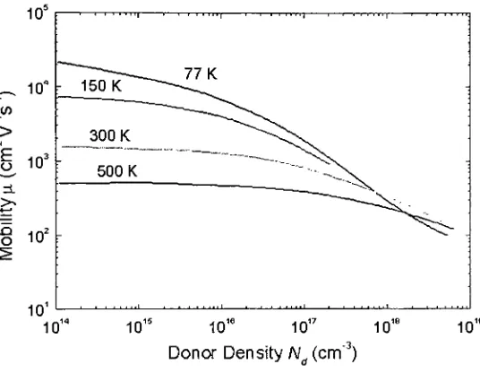
Ascanbeseen
by
figure3.2,
mobilitydecreaseswithincreasing
doping.10'
10
10*
-Ui
cn
o
-8 102
101
1 ' '""1 ' r iiiiii| r j i i ju.
77 K
r 150K
~~
"
300 K
500 K
~
""^V
-10' 10r 10" 101' 10" 101'
Donor DensityN
(cm'
[image:44.527.142.410.170.378.2])
Figure 3.2:Mobilityvs.Doping
Constant field scaling dictates that as devices are scaled
by
a parameter k thedoping
associated with the devices increasesby
1/k. This means that as devices arescaledfurtherand
further,
thedoping
associated withthe channel increases. This in turnreduces the nobility within the channel. Figure 3.2 illustrates bulk mobility, channel
mobilityis significantlyless than in thebulk dueto surface interactions andfieldeffects,
however mobility is still proportional to
doping
density. Sincethedelta-doping
planesinthe vertical MOSFET structure act as field screens, the
doping
within the channel ofthe3.5
Sii_xGex
The proposed vertical device structure incorporates
Sii.xGex
localized to thesource/drain edges of the channel region. The reason for this is to prevent the
outdiffusion of
delta-doping
into the channel with subsequentthermal steps. The majorchallenge with the use of
delta-doping
involves careful management of the thermalbudget to suppress diffusion. Because of the extreme
doping
level in adelta-doping
plane,diffusion isenhancedatlowertemperatures. Forexample, GossmanstatesthataB
delta-doping
planewilltypically
double its fullwidth athalfmaximum(FWHM)
after30min. of diffusion at 740oC [11].
However,
this outdiffusion may be suppressed forBoron
by
surrounding thedelta-doping
planewithInorGewhichinhibits diffusionofp-type dopants [16].
Therefore,
in the n-VMOS structures, a thin layers ofSiGe will bestraptheBoron
delta-doping
planetoact as adiffusion barrier.The channel region may alternately be comprised entirely of
Sii.xGex.
Thepurposeofthisis twofold.
First,
theoxidationrateofSiGealloys variesfromthatofpuresilicon. Thisallows forselective oxidationtooccur,thereforeallowingtheoxidation rate
to betailored to the devicerequirements [17].
Second,
SiGe has alarger lattice spacingthen crystalline silicon. The increased lattice spacing leads toan increase in mobilityof
bothelectrons andholes.
3.6
Metal Gate
and AdvancedGate Insulators
Deep
sub-microndevices feature gate widths in the nanometer range. Such thingates leads to large resistances. The addition ofsilicides has been used to combatthe
problem ofthis as well as contactresistances.
However,
gates are getting sothin,
thatgates should be used inorder to reduce the resistances associatedwiththe gate electrode
[9,18].
Figure 3.3 showstheITRSpredictionforgatedielectrics in futureplanardevices.
First YearofIC Production .. ..
2001 2003 2005 2007 2009 2011 2013 201S 2017
2002 2004 2006 2008 2010 2012 2014 2016
Gate Dielectric Oxideextensions
Modestk(5-10)
Mediumk(10-20) Unaryoxides
Silicates HighK(>20)
Amorphous Singlecrystal
N-doped Oxide N.
tride >v Id*;Oxyn
ZrO,,HfO
((Zr.Hf.l
LaandY
rY<__ GdjO,,SCjO,
aY)OQ SO.
1Alloys
LaAI,Os, BaZrO,, Y203,La20,
Figure 3.3: Gate DielectricRoadmap2001 [9]
The dielectrics listed in the above figure may be used in addition to
Si02
or inplaceofit. As the incorporationoftheproposed vertical MOSFETdevicewill not occur
in the near
future,
it follows that purely deposited high-k gate dielectrics will be used.The use ofdeposited gate dielectrics aids the construction of the proposed
device,
asdeposited films are often processed atlowertemperatures than those thatare grown.
3.7
Minimization oftheMiller
Overlap
Capacitance
viaSelective
Oxidation
A parasitic capacitance known as the Miller capacitance results when the gate
overlaps the source and drain [19].
Virtually
all conventional modern CMOS devicesemploy aself-aligned ion implantation using the gate and sidewall spacers as an implant
mask. In these structures, the overlap results due to the
tendency
for ions to travelunderneath thegate. This capacitance will clearly be a challenge forthe vertical devices
It is hypothesized that the
key
element forisolating
the source anddrain regionsfrom the gate, lies in the different heats of formation of semiconductor oxides. For
instance, Si02
(-204kcal/mol)
has nearly double the heat offormation ofGe02
(-119kcal/mol)
[20-26].Thus,
the channel of a transistor comprised of a SiGe layer couldconceivably have a thinner oxide layer grown than the source and drain regions. This
[1]
C.Hu,
S. C.Tam,
F.Hsu,
P.Ko,
T.Chan,
K. W.Terrill,
"Hot-Electron-InducedMOSFET Degradation
-Model, Monitor,
andImprovement,"
IEEETransactions
onElectron
Devices,
Vol.ED-32,
No.2,
February
1985.[2]
S.Ogura,
P. J.Tsang,
W. W.Walker,
D. L.Critchlow,
J. F.Shepard,
"DesignandCharacteristics ofthe
Lightly
Doped Drain-Source(LDD)
Insulated GateField-Effect Transistor,"
IEEE Transactions on Electron
Devices,
Vol.ED-27,
No.8,
August 1980.
[3]
D. J.Mountain,
D. M.Burnell,
"An Evaluation of Conventional and LDDDevices for Submicron Geometries," Solid-State
Electronics,
Vol.33,
No.5,
1990.
[4]
Kawakami,
N.;
Egusa,
K.;
Shibahara, K.;
"Reduction of threshold voltagefluctuation of p-MOSFETs
by
antimony super steep retrograde wellchannel,"
Junction
Technology,
2001. IWJT. Extended Abstracts of the SecondInternational
Workshop
on,29-30 Nov.2001,
Page(s): 7-10.{5]
Amerasekera,
A.;
Selvam, S.T.;
Chapman,
R.A.;
"Designing latchup
robustness ina 0.35 nm
technology,"
Reliability
![Figure 2.5: An Illustration of DIBL (figure adapted from [20])](https://thumb-us.123doks.com/thumbv2/123dok_us/124476.12060/26.527.179.371.214.356/figure-illustration-dibl-figure-adapted.webp)
![Figure 2.9: Mobility Enhancement for Strained Silicon MOSFETs (adapted from [21])](https://thumb-us.123doks.com/thumbv2/123dok_us/124476.12060/29.527.166.358.480.646/figure-mobility-enhancement-strained-silicon-mosfets-adapted.webp)