Rochester Institute of Technology
RIT Scholar Works
Theses
Thesis/Dissertation Collections
5-1-1995
ASIC design of an IIR digital filter: Using Mentor
Graphics DSP Station Tools
Robert Panek
Follow this and additional works at:
http://scholarworks.rit.edu/theses
This Thesis is brought to you for free and open access by the Thesis/Dissertation Collections at RIT Scholar Works. It has been accepted for inclusion in Theses by an authorized administrator of RIT Scholar Works. For more information, please [email protected].
Recommended Citation
ASIC Design of an IIR Digital Filter
Using Mentor Graphics DSP Station Tools
by
Robert C. Panek
A Thesis Submitted
ill
Partial Fulfilhnent of the
Requirements for the Degree of
MASTER OF SCIENCE
ill
Computer Engineering
Approved by:
_
Graduate Advisor - Kenneth W. Hsu, Associate Professor
George A. Brown, Professor
Roy S. Czernikowski, Professor and Department Head
Department of Computer Engineering
College of Engineering
Rochester Institute of Technology
Rochester, New York
THESIS RELEASE PERMISSION FORM
ROCHESTER INSTITUTE OF TECHNOLOGY
COLLEGE OF ENGINEERING
Title: ASIC Design of an IIR Digital Filter Using Mentor Graphics DSP
Station Tools
I, Robert C. Panek, hereby grant pennission to the Wallace Memorial
Library to reproduce my thesis in whole or part.
Abstract
Automation in VLSI design is a powerful way to simplify the VLSI layout
process and will allow for faster time to market for integrated circuit designs. One
means of automation is
VHDL,
ahardware description language for integrated circuitdesigns. Astructured VHDL description can be used to describe the hardware design
atthe logic-gate
level,
and automated software is availablethat will use thisgate-leveldesign to generate the VLSI layout. A more recent type of automation occurs at a
levelabove this. The Mentor Graphics DSP Station toolsuse ahigh-level algorithmic
description to generate the gate-level VHDL description. These tools are especially
intended for applicationsin digital signal processing
(DSP),
providingsimulation toolsparticularly geared toward DSP algorithms. One application of digital signal
processing is an infinite impulse response
(IIR)
filter. With the use of the MentorGraphics tools, a digital filterwas designed from a set of original specifications down
to the silicon level. N-well 1.2 micron CMOS
technology
with two metallayers andone polysilicon layer was used to implement the filter layout.
Using
the 1.2 micronCMOSNstandard cell
library,
the final VLSI layoutmeasured 7.315 mm x7.213 mm,Table
of
Contents
Abstract
iii
Table
ofContents
iv
List
ofFigures
viList
ofTables
viiGlossary
viiiChapter
1:
Filter Design
Concepts
1
1.1 IntroductiontoDigital Filter Design 1
1.2 Digital Filter Representations 4
1.2.1 Difference Equation 5
1.2.2 Block Diagram 5
1.2.3 Transfer Function
H(z)
61.2.4 Impulse Response
h(n)
71.2.5 Pole/Zero Plot 9
1.3 DerivationoftheBilinear Z-Transform 10
Chapter 2: MR Digital Filter Design
15
2.1 Filter
Specifications
152.1.1 Original Design
Specifications
152.1.2 Filter Order
Complexity
172.1.3
Prewarping
Filter Frequenciesto Correct for BZT 222.2 Designs BasedonNormalized Low-Pass Filter 26
2.2.1 Transformations BasedonNormalized Low-Pass Filter 27
2.2.2
Converting
H(s)
->H(z)
Using
theBilinear Z-Transform 282.2.3 Biquad-Section Design 29
Chapter 3: Mentor Graphics Automated Design
Tools
32
3.1 Introductionto Tools 32
3.2 FILlab: High-Level Filter Designand Simulation 32
3.3 Design Architect: DFLand,Schematic Editor 34
3.4 DSPlab: Simulation Tools for DFL 34
3.5 Mistrall/HDL: VHDL Generation/Compilation Tools 35
3.6 AutoLogic:
Synthesizing
VHDL-> Schematic37
3.7
DVE: Design ViewpointChecking
andValidation 383.9 IC
Station: Schematic
->VLSI Layout38
Chapter
4:
MR
Band-Reject
Filter Design Example
40
4.1 Filter
Specifications
andApplications
404.2 DFL DesignandHigh-Level Simulation 41
4.2.1 Derivation ofFilter Coefficients 41
4.2.2 DFL DescriptionofFilter 44
4.2.3 Final DFL
Simulation
Results 454.3 VHDL GenerationandCompilation 49
4.4 AutoLogic:
Synthesizing
VHDL-> Schematic 514.5 Design Architect:
Refining
Schematic 524.6 DVE: Schematic Checks andERC Validation 52
4.7 QuickSim H: VHDL SimulatioiWerification 52
4.8 IC
Station:
Schematic -> VLSI Layout 594.9
Testing
theFilter ASICChip
60Chapter
5:
Conclusions
62
References
64
Appendix A: MathCad Derivation
ofFilter
Coefficients
A-1
Appendix B: MistraH Generated VHDL
Code
B-1
Appendix
C: I/O
Schematic
For VLSI
Chip
C-1
List
of
Figures
Figure 1.1 Ideal Filter
Frequency
Response 1Figure 1.2 Digital Filter Block Diagram 6
Figure 1.3 Digital Filter Pole/Zero Plot 10
Figure 1.4 Graph ofFunctiong(a) For BZT Derivation 11
Figure 1.5 Integration Approximation fortheFunctiong(oc) 13
Figure2.1 Low-Pass Filter Prototypes forthe Four Filter Types 20
Figure 2.2 Graphical RepresentationofBZT
Mapping
23Figure2.3 Graph of
Nonlinearity
Betweens-Domain andz-Domain 24Figure 2.4
Frequency Warping
in Filter Design 25Figure 2.5 Block Diagram foraSingle Biquad-Section 30
Figure 2.6 Simplified Block Diagram for Biquad-Section 3 1
Figure 3.1 Road
Map
Through Mentor Graphics Tools 33Figure 4.1 Filter Input Test Signal 46
Figure 4.2 Filter Output Response To Test Signal 47
Figure4.3 Filter Design Example Magnitude Response
47
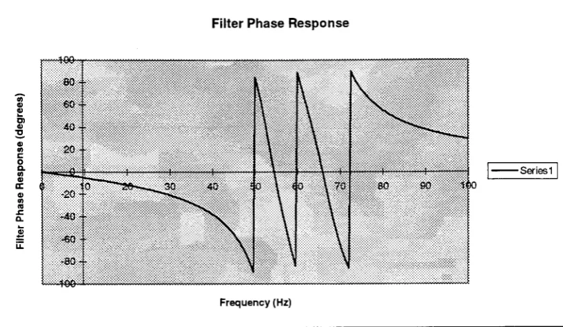
Figure 4.4 Filter Design Example Phase Response 48
List
of
Tables
Table 4.1 Filter Design Example Specifications 40
Table 4.2 Filter Design Example Simulation Results 48
Table 4.3 I/O Pin Description for Filter Design Example IC 50
Table 4.4 Bit-Serial Inputs For Digital Simulation 53
Table 4.5 msl_in Force Statements For Digital Simulation 55
Table 4.6 Digital Simulation Results 58
Glossary
ASIC Application Specific Integrated Circuit (p. 32).
Biquad-Section A two-pole/two-zero IIR filter. Two or more can be cascadedtogether to implementa higher-order filter with less error due to coefficient quantization (p. 29).
Bit-Parallel Design Separate hardware is used to process entire word-sizesat once (p. 36).
Bit-Serial Design The same hardware is reused when
processing
the bits of individual words in a design. To accomplish this, the bits of the word must be shiftedin one at atime (p. 36).
Butterworth Filter A type of analog filter whose spacing between the poles is known to be 36072n for alow-pass
filter,
where n indicatesthe number of poles. A Butterworth filter does not haveany
zeroes in thes-domain(p. 18).BZT Bilinear
Z-Transform;
used as a transformationbetweenthes-domain and thez-domain (p. 10).
DFL Design Row
Logic;
the high-levellanguage
thatis used to describe the digital filter within the DSPStation tools(p.
32).
DVE Design Viewpoint Editor (p. 38).
ERC Electrical Rules
Checking
(p. 38).Filter Gain The ratio of the magnitude ofthe output to the
magnitude of the input. The filter gain will vary
for different frequencies in adigital filter(p. 2).
Filter Order The number of polesinadigitalfilter. The order
is
an indication ofthe complexity ofthe filter (p.17).
FIR Filter Finite Impulse Response Filter (p. 3).
HR Filter Infinite Impulse Response Filter (p. 3).
Impulse Response
h(n)
The output of a digital filter when the impulsefunction isused as theinputto the filter (p. 7).
Intermediate Low-Pass Filter A filter
Hai(s)
derived from the normalizedlow-pass filter. This is an intermediate filter while
transforming
the normalized low-pass filterHan(s)
into a more complicated denormalizedparent filter Hap(s). The intermediate filter will
haveitspassband cutoff
frequency
atQc
(p. 18).LSB Least-Significant Bit (p. 49).
Magnitude Response A graph ofthe filter gain
for
the valid range ofMSB Most-SignificantBit (p. 53).
Normalized Low-Pass Filter A simplified low-pass filter
Han(s)
with apassband cutoff
frequency
of 1 rad/sec.This
canbe used as a prototype filter to derive a more
complicated denormalized parent
filter.
In thediscussion of Chapter
2,
this filter will beconverted to the denormalized parent filter
Hap(s)
in two steps, resulting in an intermediatefilter Hai(s). The normalized filter
is
alsoreferred to as a one-radian low-pass filter (p.
18).
Nyquist
Frequency
Half the sampling frequency. Thisfrequency
represents the maximum
frequency
that can bedistinguished accuratelywith digital sampling (p.
16).
Parent
Analoa
Filter The denormalized analog filterHap(s)
that adigitalfilterwillbe derived from (p. 3).
Passband The range of frequencies which are allowed to
pass through the filter without
being
suppressed(P- 2).
PhaseResponse A graph of the filter phase shift that occurs
between the output and the input for the valid
range ofinput frequencies (p. 4).
Poles of
H(z)
The values of z for which the transfer functionH(z)
equals . These are the roots of thedenominatorpolynomial of
H(z)
(p. 4).Stopband The range of frequencies which are suppressed
and not allowed to appear on the output ofthe
filter (p. 1).
Transfer Function
H(z)
The digital z-domain ratioY(z)/X(z)
describing
therelationship between the output
Y(z)
and theinput
X(z)
(p. 6).VHDL VHSIC Hardware Description Language (p. 32).
VHSIC
Very
High Speed Integrated Circuit (p. 32).VLSI
Very
Large Scale Integration (p. 32).z-Domain The digital
domain,
wherez=eje (p. 4).
Zeroesof
H(z)
The values of z for which the transfer functionH(z)
equals 0. These are the roots of theChapter
1: Filter Design Concepts
1
.1Introduction
to
Digital Filter Design
There are fourmain types offilters: the low-pass
filter,
the high-passfilter,
theband-pass
filter,
and theband-stop
filter. An ideal low-pass filteris
one that willpassinput
frequencies
less than oct to the output but block the portions ofthe input signalwith higherfrequencies from appearing at the output. High-pass
filters,
on the otherhand,
block out the lower frequencies and pass the higher ones. A band-pass filterblocks both low and high frequencies and passes only those frequencies within the
range ofthe filter specifications, while the
band-stop
filter,
sometimes called aband-reject filter or a notch
filter,
blocks only a select range of input frequencies whilepassing frequencies both below and above the stopband frequencies. The ideal filter
magnitude
frequency
response isshownin Figure 1.1 below.Ideal Low-Pass Filter
Magnitude
Frequency
ResponseIH(jco)l
CCfc
Input Signal Frequencies
Ideal High-Pass Filter
Magnitude
Frequency
j ResponseIH(jco)l
oct
InputSignal
Frequencies
Ideal Band-Pass Filter Ideal
Band-Stop
FilterMagnitude
Frequency
\ ResponseIH(jto)l
Magnitude
Frequency
j ResponseIH(ico)l
COi Oh
Input
Signal
FrequenciesInput Signal Frequencies
This
indicates
that the gain ofthe filteris
equal to one for frequencies that are passedby
thefilter
and zeroforthefrequenciesthatare rejected.Analog
filters
are useful infiltering
the input signal before it is digitized usingan analog-to-digital
(A/D)
converter. The digitized signalis
often processedby
amicroprocessor. If
instead,
a digital filter can be designed inside the microprocessor,then there isno need forthe analog filter. The noisy signal can be sent
directly
to theA/D converter, and the digitized result can be filtered
by
the microprocessor using adigitalfilter designthatisanalogous to theoriginal analog filter.
The power of digital filters in circuits comes from their flexibility. If
tomorrow, it is decided that a band-pass filter would haveworked better than a
low-pass
filter,
it iseasierto modifythefirmware code withinthe microprocessorthan it isto remove hardwired circuit parts from the circuit boards and replace them. This is
usefulbothwhile
developing
a product andenhancing it.Perhaps,
insteadofchangingto a band-pass
filter,
it is better to widen the passband of the original filter. Withcurrent
technology,
many products have remote communications ability built-in. Ifthis is so, then the microprocessor firmware can often be updated remotely without
requiring ahardwareupdate.
Another advantage of digital filters is their reliability. The results of a digital
filter are always correct for the given
input
samples. Thereis
no drift due totemperature or humidity. Because the operations are performed within a
changes, are needed. Of course, a smaller number of analog components translates
into
lower-costdesigns
also.Digital filterswillnot replace analog filterscompletely. There are cases where
it
is
not practicalforthe microprocessorto implementthe digital filter. Forexample, ifthe microprocessorisnot powerful enoughto bothmeetthe product specifications and
implement a digital
filter,
then itis
probably more expensive to use a more-powerfulmicroprocessorthanit isto usean analog filter.
Also,
there are manyapplications thatrequire a filter but have no microprocessor available to perform the digital signal
processing.
Digital filters is a major topic in the field of digital signal processing (DSP).
There are two main types of digital filters: infinite impulse response
(IIR)
filters andfinite impulseresponse
(FIR)
filters. As the name suggests, the response of aninfiniteimpulse response filter to an impulse input is of infinite duration.
Conversely,
theresponse of afinite impulseresponsefilter iszero outside of somefinitetimeinterval.
ORfilterscanbe derivedfrom
"parent"
analog filters. Atransformation canbe
performed to transform the analog filter into a digital filter equivalent. Since analog
filter design has beenresearchedin
detail,
thisprovides a solid background from whichto design IIR filters. It will be shown later that the output of an IIR filter
depends
bothon theinputsignaland feedback fromthe output signal. IIR
filters
are sometimesreferred to as recursive
filters
since the output resultis
also used as afeedback
signalThe FIR filter
is derived
purelyby
DSPtheory
and does not relate to analogfilter design. The output of an FIR filter depends only on the input signal, and this
results in some
key
advantages. An FIR filteris
always stable and can bedesigned
tohave a linearphase response. IIR
filters,
on the otherhand,
can never have alinear-phase response, and if designed so that the poles ofthe IIR filter are outside the unit
circleinthe z-domain,theIIRfilterwouldalso beunstable. The stabilityofFIR filters
is a
key
to adaptivefilters
which change their own coefficients in an intelligent waybecause it
is
not possible to create an unstablefilter.
When the signal shape isimportant to the application, then linear phase must be obtained in the filter. Data
communications is an example where linear phase response is a requirement.
However,
for voice communications applications, the linear phase response is not aconcern becausethehuman earrespondstoenergy in the
frequency
domain.IIR filter design will be discussed in this research paper in a fair amount of
detail.
However,
FIR filter design is beyond the scope ofthis paper. Both types ofdigital filters are useful for various applications.
Next,
some basic concepts to aid inthe understanding of digital filters will be presented to prepare the reader for the
discussion ofIIR filter design. These concepts are more applicable to IIR
filters
thanFIR
filters,
butthey
will provideinsight intothefieldofdigitalsignal processing.1.2
Digital
Filter Representations
There are
five
main ways to describe a digitalfilter:
create adifference
necessary to understand how to interpret these representations and how to convert
between the different
forms.
This section will discuss thesefive
different
representationsthatare referredtoinotherdigital signalprocessing sources.
1.2. 1 Difference Equation
The
first
means to describe a digital filter is through the use of a differenceequation. The difference equation specifiesthe output y(n) as a function ofthe input
x(n)and theprevious outputs as shown below:
y(n) =aox(n)+ai x(n-l) + ...+aMx(n-M)-
bi
y(n-l)-b2y(n-2) ...bN
y(n-N)x(n)
Digital
Filter ^V(n)
x(n)=inputtofilter y(n) =outputfor filter
Ifall the
bk
coefficients are zero, then we aredescribing
an FIRfilter,
withno feedbackfrom the output. Ifatleast one ofthe
bk
coefficientsis
non-zero, then an IIR filter isbeing
represented. Note that the n represents the individual digitized samples as afunction oftime, assumed to be sampled periodicallyso thatthe time between samples
is consistent. All digital filters can be represented using a difference equation; the
coefficients ak and
bk
determine the type offilterthat is implemented and the responseofthefilter.
1.2.2 Block Diagram
The logical next
step
todescribing
a filteris
tographically
represent theunderstanding filters.
Following
is
the block diagram for the difference equationpresented above:
x(n)
_a*L
A
T
J-L.
_aM_
, v(n)
A
I,
I
A
I
Time-delay
elementm
Figure 1.2 Digital Filter Block Diagram
The block diagram illustrates the recursiveness ofthe IIR filter since it is easily seen
that the current output depends on both the inputand the previous outputs. Ifall the
bk
terms were zero, then the block diagram would represent an FIR filter with nofeedback from the output signal.
1.2.3 Transfer Function
H(z)
To determine the transfer function of a digital
filter,
a simple technique is totake theZ-transform ofthe differenceequation.
Taking
theZ-transform yieldsY(z)
=X(z)
[aO+ al z-1 + ...+ aM z-M]Y(z)
[bi
z"1+
b2
z~2
+ ... +
bN
z"N]Y(z)
[1 +bj
z"1
+
b2
z"2
+ ... +
bN
z"N] =X(z)
[ao
+ ax z"1+ ... +aMz"M]
Y(z)
a0+a1z"1
+... +
aMzM
H(z)= =
X(z)
1 +bi
z"1
+
b2
z"2
+ ... +
bN
z"N
Rewriting
the equationto create positive exponentsforthe z-terms yields:Y(z)
aozM
+a,
zM~'
+ ... +aM
H(z)
= =[zN"M]
X(z)
zN
+
b,
zN"'
+
b2
zN"2+ ... +
bN
Note that often, the factor
[zN"M]
will notbe shown because most IIRfilters
have thesame number of
delay
stages for the input side as for the output side of the blockdiagram.
Thus,
sinceM=N,
[zN"M]
isequal to one and does not need to be shown inthe transferfunction.
Once the transfer function has been
derived,
the outputY(z)
can be found forany input
X(z) by
simple multiplicationinthez-domainas shown:Y(z)
=X(z)
H(z)
Next,
theimpulseresponse inthe time-domainwillbe discussed and correlated withthe transferfunction inthez-domain.
1.2.4
Impulse Response
h(n)
The impulseresponse
h(n)
is defined as theinverse
Z-transform ofthe transferfunction. It iscalled the impulseresponse because
h(n)
describes whatthe output y(n)would look likeifthe inputx(n) was a unit
impulse function.
A unitimpulse function
{
0
for n <0p(n) =
^
1 for n =0
0
for n > 0Since
theimpulse
responseis
simply the filter response to a unitimpulse
functioninput, h(n)
=y(n) whenthe
input
x(n) =p(n).As described previously, the output
Y(z)
can be computed in the z-domainby
simply multiplying the transfer function
H(z)
by
the input X(z). In general,multiplication in the z-domain is equivalent to convolution (represented
by
*)
in thetime-domain.
Thus,
as for any linear time-invariant system, the discrete outputresponsey(n)in thetime-domainisgiven
by
theequationbelow,
wherex(n)representsthe discrete inputand
h(n)
representstheimpulse response:y(n) =
x(n) *
h(n)
Using
the definition of discrete convolution results in thefollowing
two modifiedforms oftheequation above:
y(n)=
E
x(k)h(n-k)=X
h(k)
x(n-k)k=-oo k= -oo
Thus,
the impulse responseh(n)
can be used to determine the output response y(n) inthe time-domaininthe same manner as the transferfunction
H(z)
is used todetermine
the output response
Y(z)
in the z-domain. For a causal IIRfilter,
where theimpulse
response
h(n)
is
zero for n <0
(since practicalfilters
cannot predict that animpulse
1.2.5 Pole/Zero Plot
A final method of representing a filter is through a pole/zero plot in the
z-domain. Thetransferfunction
H(z)
can befactoredas shown:ao
zM + ai
zM_I
+ ... + aM
(z-zi)(z-z2)
...(z-zM)
H(Z)=
;
;
= KzN +
b,
zN"' +
b2
zN"2 + ... +
bN
(z-pi)(z-p2)
...(z-pN)
The parameters zk indicate the location of the zeroes of the filter while the pk
parametersindicate the location ofthe poles ofthefilter. Note that Kis considered to
be a gain constant. This constant will not be represented in the pole/zero plot.
However,
the filterfunctionality
is
described accurately using the pole/zero plotrepresentation. The conversion between representations of the digital filters would
vary
by
a gainconstant, but because we aredealing
with digitalfilters,
the gain can beadjusted to whatever is desirable without
changing
the operation ofthe filter. Thefilter will still pass and reject the same frequencies as it would when modeled using
one ofthe otherfourrepresentations.
Suppose thatour transferfunction was
[z-(0.2+j0.8)]
[z-(0.2J0.8)]
[z-(-!)]H(z)
=[z-0.6]
[z-(0.9+j0.1)] [z-(0.9-j0.1)]
Then,
the filter would have three zeroes and three poles. The zeroes would be at thecomplex-conjugate locations zi= (0.2 +
j0.8)
andz2 =(0.2
j0.8)
as well as at z 3=-l.
p3=
(0.9
-jO.l).
Apole/zero plotis
madeby
simply plotting the complexpoints inthez-plane as shownbelow:
i 'Im[z]
Z-plane
^
o
^^
x
j
xl Re
Unit
/
O yS
Circle
lzl = 1 ''
o Zeroesoffilter
x Polesoffilter
Figure 1.3 Digital Filter Pole/Zero Plot
As mentioned earlier, the pole/zero plot does not indicate a gain constant.
However,
all fivemethods ofrepresenting digital filters are equivalentfilter descriptions within a
gainconstant.
1
.3Derivation
ofthe
Bilinear Z-Transform
Next,
the derivation forthe Bilinear Z-Transform(BZT)
will be explained. Itis included here to
help
the reader to understand what the BZT does.Having
understood this background theory, the reader will understand why the filter
specificationfrequenciesmustbeprewarpedusingthe BZT.
The BZT
is
atransformation betweenthe continuous s-domain andthe discreteapproximation of an integrator.
Computing
the integration of afunction,
fit),
in thetime-domain
is
equivalent tomultiplying
the Laplace transform ofthatfunction, F(s),
by
afactor 1/s in the s-domain. But whatisthismultiplication factor inthe z-domain?To derive
this,
a definition ofintegration in the time domainis useful. From calculus,it
is
well knownthat theintegration of afunctionis
equivalenttodetermining
the areaunderthecurve ofthefunction withrespectto thex-axis. Supposewehave afunction
g(a)thatisto be
integrated
betweennegativeinfinity
and t.g(oc)
a
Figure 1.4 Graph ofFunctiong(a) For BZT Derivation
Integrationcanbe modeled
by
thefollowing
simpleblock diagram.g(0
J
v(t)v(t)=
J
g(a) da -ooWhen
sampling
discretely,
as in the z-domain, one can only sample at discrete pointsthroughoutthefunction.
Thus,
asamplingfrequency,
T,
mustbechosen.Thus,
if k iskT can be used as an approximation for the continuous variable t in the previous
equation.
kT
v(kT) =
J
g(a) daThisequationcan be broken down into two pieces: the contribution ofall the previous
samples taken up to the k-l51 sample and the contribution that the k* sample has
added.
kT rk-lYT kT
v(kT)=
J
g(a) da =
I
g(a) da +J
g(a) da-<~ -oo (k-l)T
Notice that the first term
is
equivalent to the function v[(k-l)T], resulting in arecursivefunction:
kT
v(kT) = v[(k-l)T]+J g(a)da
(k-l)T
Note additionally thatthesecond termis simply thearea underthe curve g(a) between
the pointsg[(k-l)T] and g(kT).
Assuming
that thesamplingperiodTis
short,then theg(a)
(k-l)T kT a
Figure 1.5 Integration Approximation forthe Functiong(a)
Thus,
the functionv(kT)canberewrittenasv(kT)=v[(k-l)T]+ T g(kT)
+ gf(k-l)Tl
Often in discrete systems, the sampling period T is understood to exist, and kT is
replacedsimply
by
k.v(k) =v(k-l) +T e(k) +s(k-l)
Thus,
the discrete integration operation has been derived. Ifthe integration operationis
discretely
appliedto the sampled function g(k), then theresultis
the discrete outputfunctionv(k).
If the Z-transform
is
applied to the previous equation, the transfer function forintegrationcan beobtained.
V(z)
=z1
V(z)
+G(z) [
1 +z"1
]
2HINTEGRATION
(Z)
=V(z)
G(z)
21+z"1
zA_
T2
z+1
z-1_
Asmentionedpreviously,the transferfunction for integration inthe s-domainis simply
equal to (1/s).
Thus,
if the transfer functions are equated, then the BilinearZ-Transform betweenthes-domain and z-domainis obtained.
_J_
2
z+ 1
z- 1
OR _2_
T
z- 1
Chapter
2:
IIR
Digital Filter Design
2.1
Filter Specifications
The
following
analysis will be taken from reference[24]
and previousknowledge offilter design.
2.1.1
Original Design
Specifications
To design a
filter,
one must know certain specifications that the filter mustmeet to suit the application. Note that these specifications may be refined to be
consistent with other goals that theusermay
have,
such as complexity. Tobegin,
thefilter that is to be designed should be selected from the four main types of
filters,
choosing a low-pass
filter,
high-passfilter,
band-passfilter,
orband-stop
filter. Theideal filterresponseforeach typeoffilterwas presented graphically in Figure 1.1.
Figure 1.1 showed what specifications are required for ideal filters. Practical
filters cannot achieve a perfect cutoff
frequency
such that the magnitude responsechangesfrom zero toone at a singlefrequency. In reality, a range mustbe specifiedin
which the filters change from a passband state to a stopband state and vice-versa.
Also,
the magnitude response of the passband is usually specified (indB)
as themaximum amount of
ripple
thatis
acceptable.Thus,
if the maximumripple
of thepassband isspecifiedtobe
0.75
dB (minimum gain =log"1
(-0.75dB
/
20)
=0.92),
thentheminimum gain and maximum gain ofthe output withrespecttothe
input
signalforSimilarly,
the magnitude response of the filter for the stopband is usuallyspecified (in
dB)
as the minimum attenuation for frequencies within the stopband.Thus,
if the minimum attenuation in the stopband is set to36
dB (maximum gain =log"1
(-36dB /
20)
=0.016),
then the maximum gain ofthe output with respectto theinput signal for
frequencies
within the stopband must be 0.016.Thus,
the realizablefilter can block out those
frequencies
of the stopband such that their effects arelimited. Note that as thefilterparameters get more stringent and the desired response
iscloserto
ideal,
thecomplexityofthefilter design increases.Once a filter type is selected, the frequencies that are relevant to the filter of
choice should beselectedas well as the desired magnituderesponse. Forexample, the
band-stop
filter can be describedby
four frequencies and two desired magnituderesponse gains. The four frequenciesofinterest includethe lower passband
frequency
(where the first passband ends), the lower stopband
frequency
(where the stopbandbegins),
the upper stopbandfrequency
(where the stopband ends), and the upperpassband
frequency
(wherethe second passband begins). As describedabove, the twodesired magnitude response gain parameters are the maximum ripple in the passband
andtheminimum attenuation inthestopband. Notethatinthepassband ofthe
filter,
it
is often desirable to have a gain of one.
Thus,
allfrequencies
that are meant to passthrough the filter do so such that the magnitude ofthe output is equal to that ofthe
inputto the filter.
Another parameter of interest when
designing
a digital filteris
thesampling
frequencies,
themaximumfrequency
in theinputsignal toadigitalcircuit should be nogreater than half the
sampling
frequency.Aliasing
occurs when a signal at onefrequency
appears to look like a slowerfrequency
signal as a result of the systemsampling rate
being
too slow to accurately reproduce the inputfrequency.
Thisaliasing is
usually unwanted. To prevent this, the samplingfrequency
of the filtershould be chosen to be at least twice the highest
frequency
contained in the inputsignal. Ifthemaximum
frequency
oftheinputsignalis
unknown, it may be possibletouse an analog low-pass filter to limitthe frequencies of the input to those which are
less thathalfthechosen
sampling
rate.To summarize, thefilter specificationsthat are required usually are specified as
passband and stopband gains as well asthe
frequency
rangesthrough which the filterisallowed to change states between passing
frequencies
andblocking
them. The nexttopic will include a discussion on how the specifications of the filter will affect the
complexityofthefilter.
2. 1.2
Filter
Order
Complexity
To designadigital
filter,
the Bilinear Z-Transform willbe used to transform ananalog filter into a digital filter. Other types of transformations that could have been
used include impulse-invariance (to create a digital
filter
with the sameimpulse
response as the parent analog
filter)
and step-invariance (to create a digital filter withthe same step response as the parent
analog
filter)
designs. The BZT method offilter. This results in a much better filter than can be created using the other two
methods.
The parent analog filter that will be used in the
following
derivations is
aButterworth filter. A Butterworth filter
is
a type of analog filter whose spacingbetween the poles is known to be 36072n for low-pass
filters,
where n indicates thenumber of poles (or the order ofthe filter). A Butterworth low-pass filter does not
have any zeroesinthe s-domain.
Given the filter parameters, the order of the Butterworth analog filter needed
to meet the specifications must be computed. To
begin,
thefrequency
parametersmust be converted from Hertz to rad/sec
by
multiplying the frequenciesby
2k(assuming
the frequencies were originally specified in Hertz). To design alow-pass,
high-pass,
band-pass,
or band-reject analogfilter,
it is sometimes easier to workbackwards to find the equivalentcomplexity one-radian low-pass filter. The order of
this normalized Butterworth low-pass counterpart will be computed,
having
apassband that ends at 1 rad/sec and a stopband
beginning
at cot as calculated in Figure2.1(a)-(d). Theresultcot willbe usedto derive an
intermediate
analog filterHaj(s)
thatcan be transformed into the more complicated parent
analog
filter Hap(s).This
parentanalog filter will then be transformed into the digital filter H(z).
Figure
2.1(a)-(d)
shows the four types ofanalog-to-analog transformations. Note once again that the
normalized prototypefilter
Han(s)
will be transformed into a parentanalog
filterHap(s)
the same
frequency
specifications as the digital filter to be designed.Thus,
if alow-pass digital filter was
being
designed,
cou would indicate the end ofthe passband andcor'
would
indicate
thestart ofthestopbandforthedigitalfilter.Case 1
:Low-Pass Filter Design
Low-Pass Filter Response Desired Low-Pass Prototype Response
Magnitude"
Response
Magnitude
'
Response
cot = COb
Figure 2. 1
(a)
Low-Pass Filter Prototype ParametersCase 2: High-Pass Filter Design
High-Pass Filter Response Desired Low-Pass Prototype Response
A 1
-a
t
Magnitude
Response
-P
^
nx'
ni. CO
Magnitude
"
Response
COr COucot'
Case 3: Band-Pass Filter Design
Band-Pass Filter Response Desired Low-Pass Prototype Response
Magnitude"
Response
cot=minimum
CO
A 1
k
^X. nitude~a
onse
-P
1 cot "
{
CO]COi(COupper+COiower COupper" COiower)+CO2" ~
COiowerCOjpper
C02(C0upper-COiower)
}
Figure
2.1(c)
Band-Pass Filter Prototype ParametersCase 4:
Band-Stop
Filter Design
Band-Stop
Filter Response Desired Low-Pass Prototype ResponseMagnitude"
Response
Magnitude'
Response
-?
CO
pper
cot=minimum
{
COl(COupper-COjower) 2
+COiOWer COupper
1 cot
C02(C0upper"
CO|OWer)
2
-CO2 +COiower COupper
CO
}
Figure
2.1(d)
Band-Stop
Filter Prototype ParametersOnce
the stopbandfrequency
cot has been calculated for the desiredlow-pass,
high-pass,
band-pass,
orband-stop
filter
as indicatedby
the four calculations above, thenthe order, n, ofthefiltercanbecomputed usingthe
following
equation:n = ceil
10(aMO) _
-1
lug
10MO)_-1
2
log
1cot
{"*10,,10)-1
"I
21og
"STJ
Notethattheceiling function indicatesthattheresult mustberounded upto an integer
value. The order, n, that theabove equation providesisthe orderthatis necessary for
the prototype low-pass filter. For low-pass and high-pass filter
designs,
the order ofthe filterwill be the same as n when the prototype filter is transformed to the desired
filter.
However,
forthe band-pass andband-stop
filterdesigns,
the order ofthe filterwill be twice the value of n when the prototype low-pass filteris transformed into the
more complicatedband-pass or
band-stop
filter.Based on the filter order, passband attenuation, and stopband attenuation, the
cutoff
frequency
Q.c
can be found that will be used to transform the normalizedlow-passanalog filter into anintermediate analog filterthatcan be used to meetthedesired
attenuation requirements. The intermediate filterwill haveits passband and stopband
altered
by
a factor ofQ.c,
resulting with the passbandending
atQ,c
and the stopbandbeginning
atQ.lc.
Note that if the result of nbefore
theceiling function is
satisfy
therequirement ofthe passband attenuation and exceed theminimum stopbandattenuation,the
following
equation should be usedtocomputeQ.c'.
The 1 inthe numeratoris the end ofthe passband for
the normalized low-pass filter that the
intermediate
cl
_,,,m(i/2n) filterwill be derived from. This
indicates
that theendofthepassband was at 1 rad/sec.
[10(a/.0)_1]
However,
if one had wanted to meet the minimum stopband attenuation exactly andexceed thepassband attenuationrequirement, then the
following
could have been usedinstead:
cot Qc2=
(1/2n)
[10(P,10)-1]
To exceedbothrequirements, one could choose a valuefor
Qc
between2C]
and Q.c2.Q.ci
<Q.C<Q.c2
ifQ.ci
<nc2
Q.c2
<Q.C<Qci
if2ci
>2C2
2.
1.3
Prewarping
Filter Frequencies
to
Correct
for BZT
Next,
the filterfrequencies
for the filter that is to be designed must beprewarped to correct for the nonlinearities ofthe Bilinear Z-Transform. The BZT is
usedto
map
thes-plane (entireplaneleftofthejco(vertical)
axis)into the unitcircle ofthe z-domain.
Mapping
aninfinite
plane into afinite
circle will cause warping thatcannot be avoided.
However,
thewarping
of thefrequencies
from the analog filterHa(s)
to thedigital filterH(z)
thatwill occurisunderstood, andifcorrections are madeBZT
Mapping:
H(z)
=Ha(s)
_2_
T
z- 1
z+1
The BZT mappingequation above canbe illustrated graphically below.
jco
Infinitely long
line ismappeds-plane tosemicircle oflength n
Im[z]
Infinitely long
line ismappedtosemicircle oflength%
Figure 2.2 Graphical Representation ofBZT
Mapping
Re[z]
As shown above, mapping an
infinitely long
line to a finite semicircle length isperformed
by
the BZT. The BZTequation presented earlier on page 14 issolved forsin terms of z. This relationship is
bidirectional,
and if it is solved for z in terms ofs,the
following
BZTequationisachieved:(2/T)
+ s z =(2/T)
- sIn the s-domain, jcocan be substituted for s without
changing
the equation.Solving
forzinterms of polar notation yieldsthefollowing:
A
(2/T)2z =
(2/T)
+jco
(2/T)
jcoJ^fy
22
jtan^ctfra)
+ (
____ _ eJ2tan"1(coT/2)
J6
2 +
(02
e-j
tanXcrfm)
where
0
=2 tan^coT^).Thus,
values for coin the s-domain thatrange from zero topositive
infinity
are mapped to an angle0
inthe z-domainbetween0
and k.Likewise,
valuesforcointhes-domain thatrange from zero to negativeinfinity
are mapped to an angle8
in the z-domain between0
and -n. The nonlinearity in this relationship isillustrated
by
thegraph ofthemappingequation as shownbelow:e
=2tan"'(coT/2)
71
CO
-7C
Figure 2.3 Graphof
Nonlinearity
Betweens-Domain andz-DomainNow,
that the nonlinear relationship between the s-domain and z-domain is understood, the next step is to look at what can be done to correct for this before applyingtheBZTequation.Suppose that we intend to design a low-pass filter that passes all
frequencies
less than cobe (band-edge
frequency),
indicating
thelow-pass
cutofffrequency
for the desired digital filteras representedby
C0u for Case 1 ofFigure 2.1 on page 19. It willalsobe assumedthat the maximum
frequency
awxwillbeless
than or equal to halfthedigital filter sampling
frequency
(Nyquist frequency).
Theanalog
inputfunction
xa(t)sampling
process. Figure 2.4 shows thefrequency
warping relationship for filterdesigns.
Frequency
SpectrumfXa(jco)
Z-domain (z=e*9)
+X(eje) =
^{x(n)}
CObe COm,
+CO
Original
Analog
Filter.
Specificationt
Ha(jto)
CO:
-?co
r-^5fe
>e
Obe
7C 271Intuitively,
one would choose at, the cutofffrequency
for the parentanalogfilter,
to be equalto CObe- When the parent analog filter is
transformed intothe desired digital filter using the
BZT equation,
frequency
warping results thatcreates an inaccurate digital filter.
Instead,
theparent analog filter should be adjusted
by
choosing a value for cct that will result in the
desired digital filteraftertheBZT
is
applied.Apply
BZTtoparentanalog filter^Ha(jco)
COfc
e
=2tan"'(coT/2)
6C
=2tan"I(abT/2)
--co <
H(eje)
+e
Figure 2.4
Frequency
Warping
in Filter DesignIt
is
desirable to design the parent analog filter so that6C
=6^.
Substituting
in this2tan"1(cqT/2)
=cflbeT2 oWT
<* =
tan(rr~
)
Thus,
whentransforming
analog filters into
digital filters using theBZTtechnique,
thefrequencies
of the parent analog filter(CObe)
should be modified using the equationabove to adjust for the nonlinearities inherent to the transformation. The resulting
frequencies
ccl should be used in place of the frequencies CObe- The requiredconversionsforthefourmaintypesarefilters are givenbelow:
Low-Passand High-Pass Filters:
_
2_
coT
^u
-tan
(
2)
Band-Passand
Band-Stop
Filters:_ 2
rCOiower
1
s "lower= ~
tan
(
2)
o -2-
AelL,
"upper
-tan
(^
2)
2.2
Designs Based
onNormalized Low-Pass Filter
When
calculating
the filter order in Section2.1.2,
the normalized low-passfilter was described as
having
its passband end at 1 rad/sec andits
stopband begin atC0f. This filterwill be transformed into an
intermediate
filterhaving
its passband end atQc
and stopband begin at2rQc.
For a filter of ordern, there are n number of poles.The poles of a filtermustbe intheleft halfofthe s-plane (inside the unit circlefor the
being
centered around the negative o axis.Thus,
for a filter oforderthree,
the polesare separated
by
60
degrees. Thefirst
poleis
atSi =-1, whilethe other two poles, s2
and S3, are at a radius one
(because
the normalized filtercutofffrequency
is
1 rad/sec)from the origin at60
degrees
from the negative a axis. The general equationfor thenormalized Butterworth low-pass filter (passband endingat 1 rad/sec)
is
shownbelow:H(s)
-*
(S
-Si)(S- s2)'"(s -s)
To transform the normalized Butterworth low-pass analog filter to the intermediate
analog filter that can be used to meet the attenuation requirements, the
following
transformation must take place in
Han(s)
using a value between2ci
andQ.c2
forQc
(from page22):
Hai(s)
=Hm(s)
This transforms the normalized Butterworth analog filter into an intermediate analog
filterthat will guaranteethat the passband and stopband attenuation specifications are
met. Thenextstep isto take thenewintermediate analog filter
Hai(s)
and convertittothedesired filtertypeas showninthenext section.
2.2. 1 Transformations
Based
onNormalized Low-Pass Filter
From Section
2.1.2,
the four types offilters
that can bedesigned
werepresented alongwith the abbreviationsforthe filterspecifications. In this section, it
is
necessaryto transform the
intermediate filter
Hai(s)
into
aparentanalog filter
Hap(s)
so2.2.1.1
Intermediate Low-Pass
-> Denormalized Low-Pass TransformHap(s)
=H.i(s)
2.2.1.2
Intermediate
Low-Pass-> Denormalized High-Pass TransformH(s)
=Hai(S)
Qu_
s2.2.1.3 Intermediate Low-Pass ->Denormalized Band-Pass Transform
Hap(s)
=Hai(s)
S "TSlowerlower""upper
S(,"upper"
Slower/
2.2.1.4 Intermediate Low-Pass-> Denormalized
Band-Stop
TransformHap(s)
=Hai(s)
Si,iiupper
-"lower/
S "T1 1lower^upper
Note that the transformation between
H^s)
andHap(s)
could have been done in onestep ifthe transformation for converting
Han(s)
toHai(s)
was combined with the abovetransformation. The parentanalog filter described
by
the transfer functionHap(s)
willnextbetransformedintothedigitalfilter described
by
H(z)
usingtheBZTequation.2.2.2
Converting H(s)
->H(z) Using
the Bilinear
Z-Transform
To converttheanalogtransferfunction intoadigital filtertransfer
function,
theBZTtechnique willbeusedas shownonce againbelow:
The resulting transfer function
H(z)
can be converted to any one of the five digitalfilterrepresentationsdescribed in Chapter 1.
2.2.3
Biquad-Section Design
Using
methods described in Chapter1,
the transfer functionH(z)
can beconverted to a
listing
ofthe poles and zeroes ofthe filter. A biquad-section uses twopoles and two zeroes.
Thus,
if one wasdesigning
a band-reject filter and originallycalculated n to be
3,
then the actual order ofthe filter is 6 (since the conversionfromnormalized low-pass to denormalized band-reject doubled the order of the digital
filter). This filter can then be divided into three cascaded
biquad-sections,
with eachbiquad-section using two poles and two zeroes from the transferfunction H(z). It is
important to pair the complex-conjugate poles together and the complex-conjugate
zeroes togetherwhen creating abiquad-section so that the coefficientsto the filterare
real-valued.
Before going into
detail,
it is important to understand why biquad-sectiondesigns are used. Biquad-section designs are used in IIR filter design because less
hardware can be used to create more accuracy. Suppose a
10-pole,
10-zero digitalfilterwas
being
designed. Thetransferfunctionwould be asfollows:
Y(z)
aoz10 + aj
z9
+ ... +a!0
(z-z,)(z-z2)"(z-Zio)
u^7\ _ _
X(z)
z10 +bi
z9 +
b2
zs
+ ...+
bio
(z-pi)(z-p2)-(z-pio)
The accuracy ofthe ten coefficients
bk
affectthe location ofthe ten poles pj. The poleApj
=KAbk
where K- io(numberofPles)Thus,
whenbuilding
a 10-pole filteras a singlestage,a slight change incoefficients (asa result of quantization of coefficients) results in a much greater shift
(1010
instead of
102)
in the pole locations than ifthe 10-pole filter is built in five cascading stages ofbiquad-sections.
A single biquad-section contains two poles and two zeroes and can be
represented
by
thefollowing
transferfunction andblock diagram:Y(z)
aoz2
+ ai z +a2
H(z)
=X(z)
z2
+
bi
z +b2
x(n) af,
X
ir
a,
4 "bl
A A
1
i '
a^ -b2
A A
1
y(n)
I
AI
Time-delay
elementFigure2.5 Block Diagram foraSingle Biquad-Section
Note that each
time-delay
element is actually a register in hardware that stores thex(n) ? a0
ai
-?y(n)
I
AI
Time-delay
elementa2
Figure 2.6 Simplified Block Diagram for Biquad-Section
This block diagram is an equivalent representation that uses two less registers per
Chapter
3:
Mentor Graphics
Automated Design
Tools
3.1
Introduction
to
Tools
In
creating
an ASIC (Application Specific IntegratedCircuit)
geared towarddigital signal processing
(DSP)
applications, Mentor Graphics has developed someautomated toolsreferred to astheDSPStation tools. These tools provide a meansfor
creating
a high-level description of a digital filter application, referred to as a DFL(design-flow
logic)
description. This high-level description can be simulated todetermine how many bits of
accuracy
are required within the filter to achieve thedesired results. Once the filter DFL has been successfully simulated, another tool can
generate the VHDL (VHSIC Hardware Description
Language,
where VHSIC is anabbreviationfor
Very
High Speed IntegratedCircuit)
forthe digitalfilter. The VHDLcan be simulated, and a schematic can be generated from the VHDL model. The
schematic can be integrated into a chip-level schematic, and this can be used to
automatically generate the VLSI
(Very
Large ScaleIntegration)
layout. To performthese steps,variousMentor Graphicstools were used as shown on the
following
page.Acompletedesign description is detailed in Chapter 4.
3.2
FILlab:
High-Level Filter Design
andSimulation
Theprogram FILlabcan beused as a
starting
pointtodesigning
adigitalfilter.
Both IIR andFIR
filters
canbe designed at ahighlevel,
andthispackage can savetheFilter
Specifications
FILlabDFL
Mistral 1
VHDL
4-DSP
Viewpoint
hdl
Compiled
VHDL
Auto-Logic
Design
Viewpoint
Design
Architect
DSP
Viewpoint
DSPlab
DFL
Modifications
Schematic Design
Architect
QuickSim U <4
Design
Viewpoint
Chip
Schematic
DVE
IC
Station
VLSI
Layout
that will be required to achieve certain filter specifications. The DFL generated may
easily
bemodifiedtochangethefiltercoefficients, if desired.3.3
Design Architect: DFL
andSchematic Editor
The DFL that is generated from FILlab may be modified using the Design
Architect program. Design Architectcan be used to both create new DFL's and edit
existing ones. This also will compile the DFL so that any syntax errors are resolved
beforesimulation.
Design Architectcan also be used as a schematic editor. The schematic that
will be generated from the VHDLcan be easily be represented as a symbol in Design
Architect. This symbol can be linked to symbols representing the VLSI chip pads.
Design Architectisusedto create and edit schematics whichcan be compiled and then
usedtogenerate theVLSI layout.
3.4
DSPlab: Simulation Tools for DFL
The DSPlab tools allowthe userto simulatethe DFLthatiscreated
by
FILlabor Design Architect. Both time-domain and frequency-domain simulations can be
performed using the DSPlab tools. This simulation software provides graphs for the
results for both ahigh-level simulation model (fullresolution of coefficients used with
maximum accuracy for both multiplications and additions) and a bit-true simulation
model (resolution of coefficients, multiplications, and additions are quantized to the
For the time-domain simulation, DSPlab allows the user to select an input
waveform. The time-domain simulation presents the input and output waveforms
graphically
as afunctionoftime.
Input waveformsmay begenerated using the built-inwaveform editor, allowing the user to enter a sine wave easily
by
specifying themagnitude, DC offset, and frequency. This inputwaveform will be connected to the
filter
input,
and the result ofthe filtercan be displayed graphically for both thehigh-level and bit-true simulation. This also allows the userto overlay the
input
waveformontheoutput waveform to observethe effects ofthefilter.
The frequency-domain simulation allows the user to select a range of
frequencies
tosweep
through the digital filter under test. DSPlab allows the user toselectthe
step
size between consecutivefrequenciestested. The resultfrom DSPlab isthe magnitude response ofthe filter. This graph illustrates the
frequency
response ofthe digitalfilter and can be used to verify that the passband attenuation and stopband
attenuations willbe met withthecurrentDFL design.
3.5
Mistral1/HDL: VHDL Generation/Compilation Tools
Mistral 1 allows the user to generate structural VHDL (as well as some other
types of netlistmodels)fromthe compiled DFL. Mistral 1 willcreate VHDL that uses
the number of bits specified in the DFL that was simulated in DSPlab.
Using
theMistral 1 analysis
tools,
the number ofdelay
stages between theinput
and output Lsgiven so that the
timing
of the VHDLis
understood. Thisinformation is displayed
The Mistral 1 tools use a concept referred to as bit-serial design to implement
theDFL design. In abit-serial
design,
thesamehardware is usedfor computingall thebits of a 12-bit operation, for example. In a bit-parallel
design,
there is hardware tohandlethe entire word size (12-bits). When values are shifted in abit-parallel
design,
theentire word size is shifted atthe sametimeto separate hardware.
However,
forthebit-serial
design,
theleastsignificantbitofthe values are shifted in first.Then,
the bitsare shifted in one at atime untilthe most-significantbit ofthe word is shifted in. The
same hardware
is
reused as the individual bits are shifted in. This results in reuse ofhardware and is more efficient, particularly for filter designs where the speed of the
results ofthebit-serial design
is
acceptable.The VHDL that is generated
by
Mistral1 can be compiled using the HDLcompiler. This compiler will compile the VHDL from the command line if the
Mistral1
library
location is specified. Thislibrary
is then linkedin,
and the compiledVHDLcanbeused
by
AutoLogic togenerate theschematicforthefilter.Note that the Mentor
Graphics
Mistral 1 tools used have not currentlyimplemented full
functionality
that the DFL syntax provides.Thus,
there are certainlimitations in the current software which restrict certain types of automation. For
example,the operators
/
(division),
div (integerdivision),
mod (integerremainder), and** (power
function)
have notbeenimplemented.
Also,
pure floating-point operationsare not supported, and
thus,
fixed-point
representations must be used. Addition andandfractional length. In Mistral
1,
delay
initializations
areignored,
so thechip
mustbeinitialized
by
preloading
thescanchainswithknownvalues.Another limitation intheMistral 1 tools is that
it
does not providetheflexibility
for filter coefficients to be scanned in and modified so that the filter operation can be
modified. On the other
hand,
Mistral 1 allows for minimizing the hardware used toimplement
a specific filter with a specific set of filter coefficients. The filtercoefficients are represented in signed digit notation (prefixed
by
Osd)
as a series ofternary
digits(0, 1,
or -1, with -1 representedby
aT)
to minimize the amount ofhardware necessary to multiply filter values
by
the coefficients. For example, 0.875can be represented as Osd LOOT (1
0.125,
since T in the third decimal positionindicates to subtract
2"3)
instead ofbeing
represented inbinary
decimal form 0.111(0.5 + 0.25 +
0.125,
where onlyaddition of2n
factors isallowed). Thisresults in one
lessoperation thatis neededtomultiply 0.875
by
another number.Thus,
thepower ofMistral 1 lies with application-specific designs where the filter coefficients are
known,
and it is desirableto minimize the hardware foruse with these coefficients. Although
the result does not provide full
flexibility
to load otherfilter coefficients, it uses muchless hardwarethanwouldberequiredtoimplementthataddedflexibility.
3.6
AutoLogic:
Synthesizing
VHDL
->Schematic
AutoLogic can be used to generate a digital schematic for a VHDL
design.
The compiled VHDL
is
loadedinto
AutoLogic,
andthe usercaninstruct
AutoLogictooptimizefor minimizingthe area required forthe layout. In
AutoLogic,
the user mustlayout.
For the design example of Chapter4,
the CMOSN 1.2 micron standard celllibrary
was used. The schematicthatresults can besaved as adesign viewpoint. Thisschematic can be used as a symbol in Design Architect and can be connected to
symbols of pads forachip design. The schematic from Design Architectcan then be
used
by
the Design Viewpoint Editortocomplete thenext step.3.7
DVE: Design Viewpoint
Checking
andValidation
The Design Viewpoint Editor
(DVE)
can be used to compile and check theschematicfor ERC (Electrical Rules
Checking)
errors. Ifno errors arefound,
adesignviewpoint is generated for the schematic. This design viewpoint can be used to
simulatethedesignat abit levelandfor automatically generatingtheVLSIlayout.
3.8
QuickSim II: VHDL Simulation/Verification
QuickSim II allows the user to simulate the design viewpoint that has been
generated from the VHDL. This allows the user to control the signals on the input
pads and observe the signals on the output pads of the chip. The input signals,
however,
mustbe specified asforces,
eitherlow orhigh,
and the times that the signalschange state.
Simulating
a filterat the bit-level for a bit-serial design istedious,
butthis was performedin the designexample in Chapter 4to ensure that the
timing
ofthechipwasunderstood.
3.9
IC Station:
Schematic
->VLSI
Layout
Once there
is
confidence that the designis
correct, ICStation
can be used toprogram to generate afloorplan forthe chip, place the ports
(pads)
forthe chip, placethe standard cellsfrom the
library
choseninAutoLogic,
and complete the routing forChapter 4: IIR Band-Reject Filter
Design Example
4.1
Filter
Specifications
andApplications
In this chapter,aband-reject filterthat canblockout
60
Hz frequencieswill bedesigned so that the VLSI layoutcan begenerated. The chosensampling
frequency
is3000
Hz. The parametershave been chosen suchthatasix-pole, six-zero filterwillberequired. The designspecifications are summarized below:
Parameter Design Specification ;
Sampling Frequency
3000 HzLower Passband
Frequency
50 HzLowerStopband
Frequency
58 HzUpperStopband
Frequency
62HzUpper Passband
Frequency
72 HzMaximum Passband Ripple 0.75 dB
Minimum Stopband Attenuation 36 dB
Inputand Output Representations 8 bits
Table4. 1 Filter Design Example Specifications
This filterpresents some uniqueapplications. In the United
States,
A/C poweris
delivered from utilities using 60 Hz waveforms. The 60 Hzfrequencies
thatare thesource of power in so
many
applications also cause noise within these systems. Itis
sometimes useful to block out the
60
Hz noise,especially
if the applicationis
concerned at
looking
at a signal thatis
not supposed to containany
60
HzIn most power-quality applications, harmonic distortion is considered to be
undesirable. Ifthe voltage signalfora residence
is
being
monitored forpower-quality,then one would desire that the waveform contain only a 60 Hz component ideally.
There are ways to measure total harmonic
distortion,
but one application might be tofeedthe digitizedvoltagesignalthrough a60-Hz bandreject
filter,
and whateversignalis leftcontainsmostly theharmonic distortion whichcanbe analyzedfurther.
4.2
DFL Design
andHigh-Level Simulation
To begin
initially,
FILlab was used to get a general idea ofthe complexity ofthe filter that is required to meet these specifications. FTLlab generated a DFL
description,
whichwas modifiedtocontainthecoefficientsthatwillbe derived next.4.2. 1
Derivation
ofFilter
Coefficients
A complete derivation of the filter coefficients is presented in Appendix
A,
containing the MathCad printout of the design steps described in Chapter 2. The
coefficientsforthe three biquad-sectionswere derived usingthe stepsfrom Chapter 2.
In addition, Appendix A describes some quantization issues which will also be
discussed next.
Afterthebiquad-section coefficients were
derived,
the effects ofquantizingthecoefficients needed to be analyzed.
Quantizing
the coefficients canseverely
affect thefilter performance. In a digital
filter,
the coefficients need to be quantized, but asmentioned in Section 2.2.3
concerning
thebiquad-sectionfilter
design,
slight variationsbiquad-section
approach. The gain ofthe filter withfull precision wasdesigned
to beunity.
However,
after quantizing the coefficients, the gain of the filteris usually
greater than one as a result of the change in pole locations ofthe
filter.
Ifthe filtergain istoo much greaterthanone, thenit may be a requirementthatthe output contain
more bits than the input. In this particular
design,
the input and output both will berepresented
by
8-bits,
and thus, it is importanttokeep
the filtergain less than or equalto one. In Appendix
A,
the filter was set up to meet the stopband attenuation andexceed the passband a