Visualization of Di
ff
usion within Nanoarrays
Yang Liu,
†Angelika Holzinger,
‡Peter Knittel,
‡Lukasz Poltorak,
§Alonso Gamero-Quijano,
§William D. A. Rickard,
∥Alain Walcarius,
§Gre
goire Herzog,
́
*
,§Christine Kranz,
*
,‡and Damien W. M. Arrigan
*
,††Nanochemistry Research Institute, Department of Chemistry and∥John de Laeter Centre, Curtin University, GPO Box U1987,
Perth, Western Australia 6845, Australia
‡Institute of Analytical and Bioanalytical Chemistry, Ulm University, Albert-Einstein-Allee 11, 89081 Ulm, Germany
§Laboratoire de Chimie Physique et Microbiologie pour l’Environnement (LCPME), UMR 7564, CNRS, Universitéde Lorraine, 405
rue de Vandoeuvre, 54600 Villers-les-Nancy, France
*
S Supporting InformationABSTRACT: The direct experimental characterization of diffusion processes at nanoscale remains a challenge that could help elucidate processes in biology, medicine and technology. In this report, two experimental approaches were employed to visualize ion diffusion profiles at the orifices of nanopores (radius (ra) of 86±6 nm) in array format: (1) electrochemically assisted formation of silica deposits based on surfactant ion transfer across nanointerfaces between two immiscible electrolyte solutions (nanoITIES); (2) combined atomic force - scanning electrochemical microscopy (AFM-SECM) imaging of topography and redox species diffusion through the nanopores. The nature of the diffusion zones formed around the pores is directly related to the interpore distance within the array. Nanopore arrays with different ratios of pore
center-to-center separation (rc) to pore radius (ra) were fabricated by focused ion beam (FIB) milling of silicon nitride (SiN) membranes,
with 100 pores in a hexagonal arrangement. The ion diffusion profiles determined by the two visualization methods indicated the formation of overlapped or independent diffusion profiles at nanopore arrays withrc/raratios of 21±2 and 91±7, respectively.
In particular, the silica deposition method resulted in formation of a single deposit encompassing the complete array with closer nanopore arrangement, whereas individual silica deposits were formed around each nanopore within the more widely spaced array. The methods reveal direct experimental evidence of diffusion zones at nanopore arrays and provide practical illustration that the pore−pore separation within such arrays has a significant impact on diffusional transport as the pore size is reduced to the nanoscale. These approaches to nanoscale diffusion zone visualization open up possibilities for better understanding of molecular transport processes within miniaturized systems.
U
nderstanding diffusion of chemical species from pores and channels is of great importance in many fields, ranging from the transport of ions of biological interest through membrane channels1,2and single DNA molecule analysis3,4to membrane-supported reactions5 and transdermal drug deliv-ery.6 The development and applications of nanoporous membranes have attracted considerable interest in recent years, but require a better understanding of mass transport at the nanoscale, which remains a theoretical and experimental challenge of particular relevance to thefield of nanofluidics.7,8 As the size of pores decreases to the nanoscale, interesting mass transport behavior has been observed, such as nonlinear ionic transport, due to the high flux of charged species,7 and significant deviations from ideal behavior, which can be interpreted in terms of the dynamic diffuse double-layer effect.9 In many cases, diffusion measurements at nanoporous arrays are averaged over the whole or a large section of the membrane, assuming that the nanopores are equivalent within thearrays.10,11 However, as reported on electrochemical micro-arrays, radial diffusion at adjacent electrochemical interfaces can become overlapped (interacting) if the separation distance between interfaces is insufficient. This behavior significantly impacts the performance of devices designed for parallel measurements in liquids.12−14In recent decades, mass transport behavior at microelectrode arrays has been extensively studied both theoretically and experimentally,15−18leading to a design criterion with rc > 20ra (rc, center-to-center distance; ra, disc
electrode radius). However, at electrochemical nanointerface arrays, whether solid electrodes or liquid−liquid interfaces,10,11 this design criterion is not valid. Both experimental measure-ments of electrochemical current andfinite element modeling of diffusion processes have indicated that nanointerface arrays
Received: February 5, 2016 Accepted: June 4, 2016 Published: June 4, 2016
Article
must have larger rc/ra ratios in order to achieve maximum performance. Whereas electrochemical currents and modeling13 have been employed to understand the behavior of such arrays, experimental visualization remains challenging due to the lack of effective tools and only a few attempts have been made to observe diffusion zones at nanopore arrays.19−27
It is highly desirable to visualize diffusion behavior at nanoarrays,28−30as this will enable a direct observation of the process and help understanding of ion transport at the nanoscale. This, in turn, removes the sole reliance on theoretical models that may include approximations and assumptions.11,31,32 Additionally, effective experimental meth-ods to visualize ion diffusion in liquids would enable the straightforward study of complex nanosystems, for which development of appropriate theoretical models might be difficult. Poltorak et al. reported the in situ formation of silica
films at arrays of microinterfaces between two immiscible electrolyte solutions (microITIES) based on surfactant ion transfer across the interfaces, thus visualizing radial diffusion within such microarrays.33−35 Furthermore, combined atomic force microscopy and scanning electrochemical microscopy (AFM-SECM) was applied to visualize redox-active species diffusing at an array electrode compromising closely spaced microdiscs.19,20 Regarding diffusion through nanopore mem-branes, Shen et al. imaged ion transport through highly porous nanocrystalline silicon membranes by high-resolution SECM, demonstrating that the structural parameters of the nanopores were consistent with those determined by transmission electron microscopy (TEM).21 Macpherson et al. used a Pt-coated silicon AFM tip to probe the diffusional transport of redox-active species at nanoporous polycarbonate membranes.22 Kueng et al. reported an AFM-SECM tip-integrated biosensor for simultaneous imaging of surface morphology and glucose transport through a porous membrane.23Finally, Baker’s group investigated ion transport through single nanopores within track-etched multipore membranes using scanning ion conductance microscope (SICM), which exhibited high resolution.24−27 While these methods realized the in situ visualization of ion diffusion through submicron and nanosized pores, they focused on transport through randomly distributed pores, which behaved like independent single nanopores. Furthermore, while it is known from simulations that diffusion at regular arrays of nanopores exhibited different behavior depending on the pore−pore separations,11there have been no reports of the visualization of the diffusion profiles within such an ordered array of nanopores.
In this work, the aim was to demonstrate experimental approaches that allow direct visualization of diffusion processes occurring at the orifices of nanopores in regular arrays. Two such approaches are reported: the deposition of silica on arrays of nanoITIES using the diffusion of surfactant ion transferred from organic to aqueous phases as the deposition template, and the simultaneous imaging of topography and diffusion (of Ru(NH3)63+) across an unmodified nanopore array by a
combined AFM-SECM approach. These methods were used to visualize diffusion at nanopore arrays, which were prepared by focused ion beam (FIB) milling of silicon nitride (SiN) membranes10,36to provide regular nanopore (ra= 86±6 nm)
arrays of two designs (rc/ra= 21±2 or 91±7). It was found that the pore center-to-center separations had a significant impact on diffusion within the arrays. At the closer-spaced arrays (rc/ra= 21 ±2), the silica material modified the entire array and the local currents measured by AFM-SECM showed
an overlapped diffusion zone above the array. In contrast, individual silica hemispheres and equivalent current signals were observed at the more widely spaced arrays (rc/ra= 91 ± 7), demonstrating the presence of independent diffusion. These observations provide direct experimental evidence for the distinctive diffusion behaviors at nanoarrays, which are in good agreement with previous simulation predictions. Thus, the strategies reported here now enable a straightforward under-standing of diffusion in complex systems at the nanoscale without reliance on simulation models, and open up new opportunities for the development of efficient nanosystems, from elementary nanomaterials to complete nanodevices.
■
EXPERIMENTAL METHODSThe silicon nitride (SiN) membranes with thickness of 50 nm were purchased from SIMPore Inc. Arrays of 10 × 10 nanopores (ra= 86± 6 nm) arranged in a hexagonal pattern
with varyingrc were fabricated and characterized with a dual beam focused ion beam-scanning electron microscope (FIB-SEM) instrument (Zeiss Neon 40EsB, Carl Zeiss Nano Technology Systems, Oberkochen, Germany). All pores were milled using a Ga+ion beam with an accelerating voltage of 30
kV and a beam current of 50 pA.
Silica materials were deposited at the nanoITIES supported by a SiN nanopore array membrane following a previous procedure.33,34In the aqueous phase, tetraethoxysilane (TEOS) was hydrolyzed in a solution of 5 mM NaCl. The hydrolysis was performed at pH = 3 with stirring for 1 h. These conditions ensured hydrolysis of TEOS precursors and avoided silica condensation.37Prior to the formation of the ITIES, the pH of the aqueous phase was increased to 9 in order to facilitate silica condensation. The organic phase consisted of bis-(triphenylphosphoranylidene)ammonium tetrakis(4-chlorophenyl)borate (BTPPATPBCl) as the organic electrolyte and cetyltrimethylammonium tetrakis(4-chlorophenyl)borate (CTATPBCl) as the template species, both dissolved in 1,2-dichloroethane (DCE). Electrochemical deposition of silica was implemented at the nanoITIES arrays based on the following electrochemical cell: Ag|AgCl|300 mM TEOS + 5 mM NaCl in H2O∥14 mM CTATPBCl + 10 mM BTPPATPBCl in DCE|Ag. The scan rate was 5 mV/s. Silica deposition was followed by heat treatment at 130°C for 16 h to ensure cross-linking. The removal of template species present inside the silica pores was effected by either (i) calcination at 450 °C for 30 min or (ii) stirring in ethanol containing 0.1 M HCl for 2 h.
AFM-SECM probes were fabricated following the procedures described elsewhere.38,39 Nonmetallized silicon nitride probes (Olympus) were modified with a 100 nm gold layer and then insulated with silicon nitride (PECVD). A frame-shaped gold electrode (approximately 600 nm in diameter) was exposed at the truncated AFM tip via FIB milling. A conical conductive tip of Pt/C was then deposited onto the exposed electrode using ion-beam induced deposition (IBID) using a square-shaped pattern (edge length 1μm) with typical heights in the region of 466 nm. The deposited Pt/C was then reshaped and sharpened via FIB to obtain curvature radii in the range of 20−25 nm (Figure S1A). The electrochemical response of the conical AFM-SECM probe was characterized by cyclic voltammetry in deaerated 5 mM Ru(NH3)6Cl3in 0.1 M KCl at a scan rate of
0.1 V/s (Figure S1B).
SEM images of the silica deposits were obtained with a dual beam FIB-SEM Helios Nanolab 600 microscope (FEI, Eindhoven, NL). AFM imaging of the silica structures was
performed with a Bruker Bioscope Catalyst (Bruker, Germany). The silica deposit at the nanopore array exhibiting individual diffusion profiles was imaged in PeakForce Tapping (PFT) mode at a frequency of 1 kHz with an amplitude of 300 nm using a SNL probe (Cantilever C,k = 0.35 N/m, tip height: 2.5−8 μm, Bruker, Germany), whereas the deposit obtained from overlapped diffusion was scanned at a frequency of 0.5 kHz with an amplitude of 2μm using a RTESP probe (k= 5 N/m, tip height: 10−15μm, Bruker, Germany) accounting for the feature height. High-resolution images of the pore arrays prior to silica modification were obtained using a FIB-sharpened NCL probe (k = 47 N/m, NanoWorld) in tapping mode, which is able to penetrate the membrane pores.
AFM-SECM measurements were performed in AFM contact mode, while simultaneously imaging the flux of Ru(NH3)63+
through the SiN nanopore arrays. Experiments were performed in 0.1 M KCl solution using an electrochemical AFM cell with a three-electrode setup: the integrated Pt/C AFM-SECM probe as working electrode, a Ag/AgCl reference electrode and a platinum (Pt) counter electrode. The reduction of Ru(NH3)63+
was detected at−0.3 V versus Ag/AgCl (Figure S2).
■
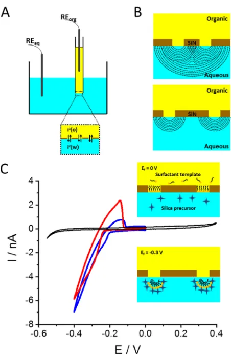
RESULTS AND DISCUSSION [image:3.625.331.557.63.412.2]The electrochemically assisted generation of silica deposits at liquid|liquid interfaces provides an effective way to visualize diffusion behaviors, as the formation of silica in the aqueous phase depends on the transfer of surfactant ion from the adjacent organic phase.35The driving force is the accelerated condensation of TEOS in the presence of cationic surfactants, due to favorable electrostatic interaction with the negatively charged silica monomers, leading to the self-assembled condensation of a surfactant−silica hybrid material.40 Figure 1A illustrates the experimental arrangement for electrochemical silica deposition at the nanoITIES arrays formed at the nanopore arrays. The schematic views of the expected interfacial diffusion profiles at the nanopore arrays with different ratios rc/ra (21 ± 2 and 91 ± 7) are indicated in Figure 1B. In order to generate silica materials on these nanoITIES arrays, cetyltrimethylammonium (CTA+), which functions as both condensation catalyst and template, was present in the organic electrolyte phase, and the hydrolyzed form of the silica precursors (TEOS) was present in the aqueous electrolyte phase. Driven by the potential difference at the polarized interfaces, CTA+ can transfer across the
nanoITIES where it diffuses into the aqueous phase, exhibiting overlapped or independent diffusion profiles at the arrays with smaller or larger ratios rc/ra, respectively. Thus, the CTA+
diffusion zones established at the arrayed nanoITIES serve as the template for the formation of silica deposits, which in turn enables their visualization.
Figure 1C shows the cyclic voltammograms for the generation of the silica materials on the nanoITIES supported by the nanopore arrays withrc/raof 21±2 (red curve) and 91 ±7 (blue curve). The black curve was recorded in the absence of precursor and template, and indicates the potential window is limited by the background electrolyte ion transfers. Regarding the deposition of silica, the schematic diagrams inset inFigure 1C illustrate the silica formation processes. At 0 V, the interface was covered with a monolayer of CTA+.34As the potential was scanned from positive to negative potentials, at about−0.3 V the cationic template CTA+transferred from the organic phase to the aqueous phase, and the current continuously increased rather than reaching a limiting current plateau after the ion
transfer wave, as observed for other transfers at such nanoITIES arrays.41 Under such conditions, the local concentration of CTA+ transferred to the aqueous phase exceeded its critical
micelle concentration, enabling the formation of charged micelles whose presence facilitated the condensation of the TEOS precursor around the surfactant template, which resulted in silica deposition on the aqueous side of the nanoITIES.34On the reverse voltammetric scan, a characteristic positive peak located at about 0.15 V was observed, which was attributed to the back transfer of CTA+to the organic phase, followed by an abrupt drop of current due to the limited amount of CTA+
available in the aqueous phase. Furthermore, the reverse faradaic peak current, related to the concentrations of CTA+
transferred back to the organic phase, was greater at the closer-spaced array (red curve) than that at the larger one (blue curve). This can be attributed to the fact that at closer-spaced arrays, the flux away from the interfaces is lower (due to overlapped diffusion zones),10so that more CTA+builds up in
Figure 1.(A) The experimental arrangement for electrochemistry at nanoITIES supported by nanopore arrays. The aqueous phase is represented in blue and the organic phase in yellow; REorg, reference
electrode for the organic phase; REaq, reference electrode for the
aqueous phase; iz, ionic species of chargezin the organic phase (o) or
in the aqueous phase (w). (B) Schematic views of the diffusion profiles established at the nanopore arrays withrc/raof 21±2 (upper) and 91 ± 7 (lower). (C) Cyclic voltammograms, with schematic diagrams representing the formation of surfactant-templated silica materials, at nanoITIES arrays withrc/raof 21±2 (red curve) and 91±7 (blue
curve); a blank cyclic voltammogram recorded in the absence of silica precursor and surfactant template is also shown (black curve). Scan rate: 5 mV/s.
the vicinity of the interfaces and, as a result, the local concentration is higher prior to transfer back to the organic phase.42−44 Previous studies have shown that the amount of CTA+ions trapped within the silica deposit increased with the thickness of the deposit,25 also consistent with the higher reverse transfer current.
Figure 2 shows the SEM images of the two array designs before and after modification with silica.Figure 2A and C show
the images of the arrays with the ratiorc/raof 21±2 and 91± 7, respectively. The radii within each array were 86± 6 nm, based onfitting a circle to the image of the nanopore, indicating an acceptable precision for practical experiments. The silica materials were formed at the nanoITIES arrays based on the electrochemical CTA+transfer from organic to aqueous phase. Two post-treatment procedures, calcination at 450 °C or stirring in ethanol containing 0.1 M HCl (reagent treatment), were applied to remove the template species present inside the silica pores. Figure 2B and D indicate the silica-modified nanoarrays obtained by calcination and reagent post-treatment, withrc/raof 21±2 and 91±7, respectively. It can be observed
that the silica deposit, which was displaced from the original area to some extent, covered the entire array for the closer-spaced pores (rc/ra= 21±2;Figure 2B), which is attributed to the overlap of surfactant diffusion zones formed in the aqueous phase. The particles dispersed on the surface of the SiN membrane might be salts and carbon formed in the calcination process. However, at the more widely spaced array (rc/ra= 91 ± 7), uniform distribution of the silica deposits at each individual nanopore can be observed (Figure 2D), which is indicative of the formation of independent surfactant diffusion zones in the aqueous phase.
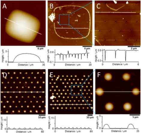
Topographic information about these silica-modified nano-arrays was obtained by AFM characterization.Figure 3A and B show the silica materials formed at the nanoITIES arrays with
rc/ra of 21 ± 2 via calcination and reagent post-treatment, respectively. The height profile along the white line indicates
that the silica deposit is semielliptical with a maximum height of 4.1μm (Figure 3A). The shape of the silica deposit from the top view is close to a 25×23μm2rectangle, which covered the entire 15× 13μm2area of the nanopore array. This can be
attributed to the significant overlap of the diffusion zones at the closer-spaced nanopore arrays. However, it must be noted that at microITIES arrays with similar ratios rc/ra of 20, silica
[image:4.625.65.298.163.379.2]modification of the individual micropore orifices was obtained,34 indicating that the diffusion processes behave differently at arrays of nanoscale and microscale pores. In a further imaging experiment, the nanopores under the silica deposit (i.e., from which the silica cap was displaced) were imaged using a high-aspect ratio AFM tip with a tip curvature radius below 5 nm (Figure 3B). In the height profile (below
Figure 3B), there are 10 downward spikes, which correspond to the number of nanopores in a line of the array. Thus, the AFM characterization can provide further information about the nanopore arrays after silica deposition. Figure 3C shows a magnified area of the nanopore array under the silica cap, indicating that some of the nanopores were blocked (height profile shown belowFigure 3C), perhaps due to the ineffective removal of species involved in the reaction. Unblocked pores show depth values larger than the expected 50 nm (membrane thickness), which indicates that the tip penetrates through the pores. As the membrane is freestanding, the obtained depth values larger than 50 nm are due to the AFM tip sides hitting the pore walls. The silica materials formed at the nanoITIES arrays of ratio rc/ra of 91 ± 7 and with postdeposition calcination or reagent treatment are shown inFigure 3D and E, respectively.Figure 3F shows a magnification of some of the silica deposits fromFigure 3E. It can be seen from the height profiles (below each image) that hemispherical silica deposits were formed on each nanopore. These deposits had radii of about 1.6±0.1μm (n= 10), as determined from the line scans shown underneathFigure 3D−F.
Figure 2.SEM images of the nanopore arrays withrc/raof 21±2 (A)
and 91 ± 7 (C), and the corresponding silica-modified nanopore arrays obtained from (A) and (C) following calcination (B) and reagent (D) post-treatment, respectively. Note the difference in scale bars.
Figure 3.AFM height images of the silica-modified nanopore arrays withrc/raof 21±2 (A, B) and 91±7 (D, E) obtained by calcination
(A, D) and reagent post-treatment (B, E). (C) and (F) indicate the magnified area shown in the dashed boxes of (B) and (E), respectively. The corresponding height vs distance profiles marked by the white lines are shown below each image.
Theoretically, the nanoITIES formed at the orifices of the nanopores behave like an inlaid disk electrode,36,42 and the thickness of the diffusion layer (δ) can be estimated according to the equation45
δ= 2Dt (1)
where D and t are the diffusion coefficient and time, respectively. In this work, a typical value of D for CTA+
diffusion in the aqueous phase is 0.95 × 10⁻⁷ cm2 s−1,34
so that the resulting thickness of the diffusion layer for CTA+
transfer at a scan rate of 5 mV/s is about 37μm (diffusion time = ca. 80 s), which is greater than the size of silica materials formed at either nanoarray dimensions used in this study. This discrepancy may be related to a number of factors including a change in solution properties upon silica formation, (e.g., changes in local viscosity), and the fact that CTA+ aggregates have a diffusion coefficient at least 1 order of magnitude lower than that of monomeric CTA+.46
These factors contribute to a lower diffusion rate away from the nanoITIES, so that the diffusion zone size from imaging of silica deposition is lower than that predicted byeq 1.
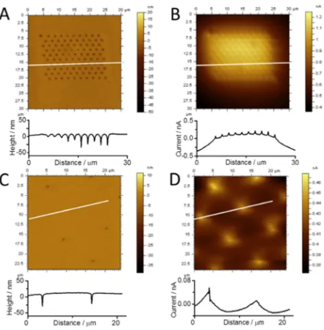
The formation of silica at nanoITIES arrays provided an ex situ method to visualize the diffusion zones within nanoarrays, as the morphologies of the electrochemically generated silica reflect the diffusion of surfactant ions in the aqueous phase. In order to realize in situ visualization, another approach based on AFM-SECM measurements was applied, which also can confirm the diffusion zone behavior at the nanoarrays with different pore center-to-center separations. In this case, no silica was deposited. A conical Pt/C tip with a tip curvature radius of 20 nm was employed as the AFM-SECM probe to image simultaneously the morphology of the unmodified nanopores and the diffusion of 20 mM Ru(NH3)63+through the nanopore
arrays. The nanoarray membranes were used to separate a lower compartment (donor compartment),filled with aqueous electrolyte solution containing the redox species, from the upper compartment,filled solely with electrolyte solution. The Pt/C AFM-SECM probe was biased at a potential of−0.3 V (vs Ag/AgCl), to reduce Ru(NH3)63+ to Ru(NH
3)62+, in order to
visualize ion transport through the nanopores. The topography images of the nanoarrays withrc/raof 21±2 (Figure 4A) and
91±7 (Figure 4C) imaged in AFM contact mode indicate that the size of the nanopores measured from the height profiles is consistent with that obtained from SEM images (Figure 2), although the shape seems to be slightly distorted by the tip geometry. The electrochemical current map at the arrays with the closer nanopore spacing (Figure 4B) exhibits an increased current over the array, with a decreasing current gradient toward the edges of the array. This provides a direct visualization of the overlapped diffusion zones of Ru(NH3)63+
as the ions diffuse from the nanopores into the bulk solution (Figure 4B). Also, it is clearly visible that at the individual pores (see height profile below Figure 4B), a current spike is observed, which can be explained by the penetration of the Pt/ C tip into individual nanopores (Figure S3), which causes an enhanced concentration profile at the tip apex, and hence an increased current. Taking the tip geometry into account, a length of about 112 nm would penetrate the pore, resulting in an estimated current (id) of about 0.4 nA based on the
following equation for conical electrodes (eq 2),47
= ⎡ + ⎜ ⎟ ⎣
⎢ ⎛⎝ ⎞⎠ ⎤⎦⎥
i nFDc a q h a
4 1
p
d 0
(2)
wherenis the number of electrons,Fis Faraday constant,Dis the diffusion coefficient (5.48×10⁻⁶cm2/s for Ru(NH3)63+),48 c0is the bulk concentration, andaandhare the radius and the height of the cone, respectively (q= 0.3661,p= 1.14466).
The experimentally determined current due to the penetration of the tip into the pores was about 0.1 nA, which is the same order of magnitude as the predicted current (eq 2). The observed discrepancy is attributed to an imperfect cone shape of the prepared tip (Figure S1A) and, hence, a possibly altered penetration depth, and to the impact of tip movement on mass transport within the nanopores, both factors which were not taken into account ineq 2. At the array with larger pore center-to-center spacing (rc/ra of 91 ± 7), individual current profiles can be observed that decreased nearly to zero in the space between adjacent pores (Figure 4D). Again, when the conical tip penetrates the pores, an increased current similar to that observed at the array with closer pore spacing is observed. This illustrates the achievement of independent diffusion zones at the nanopores in the array (Figure 4D). The results show that in situ study of mass transport at nanopore arrays can be realized in terms of visualization of the diffusion processes in liquid simultaneously with topography, supporting the visual-ization of diffusion profiles by the silica deposition strategy discussed above.
■
CONCLUSION [image:5.625.327.563.67.307.2]In summary, two approaches to visualize diffusion within arrays at the nanoscale were demonstrated, either ex situ monitoring the morphology of silica deposited on the nanoITIES arrays or in situ detection of ion diffusion profiles at the arrayed nanopores. Two nanopore arrays with hexagonal arrangements
Figure 4. AFM height (A, C) and electrochemical current (B, D) images of unmodified nanopore arrays withrc/raof 21±2 (A, B) and
91±7 (C, D), recorded with a Pt/C AFM-SECM probe. Faradaic current resulted from the reduction of Ru(NH3)63+diffusing through
the nanopores. The corresponding height or current signal vs distance along the white lines is illustrated below each image.
in SiN membranes with rc/ra of 21 ± 2 and 91 ± 7 were successfully fabricated by FIB milling. Using the experimental visualization strategies of silica deposition or electrochemical imaging, it was found that diffusion from the arrayed nanopores exhibited different behaviors depending on the pore−pore spacings within the arrays. Thus, either overlapped diffusion profiles at arrays with smaller pore−pore spacings or independent diffusion profiles at arrays with larger pore center-to-center separations were observed. These visualization methods provide direct visual evidence of the impact of pore− pore separations on radial diffusion at the nanoscale and open up an experimental basis for in-depth understanding of mass transport behavior within nanoarrays.
■
ASSOCIATED CONTENT*
S Supporting InformationThe Supporting Information is available free of charge on the
ACS Publications website at DOI: 10.1021/acs.anal-chem.6b00513.
Figures S1−S3 (PDF).
■
AUTHOR INFORMATIONCorresponding Authors
*E-mail: gregoire.herzog@univ-lorraine.fr. *E-mail: christine.kranz@uni-ulm.de.
*E-mail: d.arrigan@curtin.edu.au. Phone: +61892669735.
Notes
The authors declare no competingfinancial interest.
■
ACKNOWLEDGMENTSThe authors thank the Australian Research Council (Grant DP130102040), the Deutscher Akademischer Austausch Dienst (DAAD; Project 57060632), the Agence Nationale pour la Recherche (Grant No. ANR-14-CE14-0002-01), and the Joint Research Cooperation Scheme of the Australian Technology Network and the DAAD (Travel Grant) for funding. The Focused Ion Beam Centre UUlm (supported by FEI Company, Eindhoven, The Netherlands, German Science Foundation (Grant INST40/385-F1UG) and Struktur- und Innovations-fonds Baden-Württemberg) and Curtin University’s John de Laeter Centre (partially funded by the University, and the State and Commonwealth Governments) are thanked for access to facilities.
■
REFERENCES(1) Matsuda, H.; Saigusa, A.; Irisawa, H.Nature1987,325, 156−159. (2) Goulding, E. H.; Tibbs, G. R.; Liu, D.; Siegelbaum, S. A.Nature
1993,364, 61−64.
(3) Kim, M. J.; Wanunu, M.; Bell, D. C.; Meller, A.Adv. Mater.2006,
18, 3149−3153.
(4) McNally, B.; Singer, A.; Yu, Z.; Sun, Y.; Weng, Z.; Meller, A.
Nano Lett.2010,10, 2237−2244.
(5) Dryfe, R. A. W.; Simm, A. O.; Kralj, B.J. Am. Chem. Soc.2003,
125, 13014−13015.
(6) Prausnitz, M. R.; Mitragotri, S.; Langer, R. Nat. Rev. Drug
Discovery2004,3, 115−124.
(7) Krapf, D.; Quinn, B. M.; Wu, M.-Y.; Zandbergen, H. W.; Dekker, C.; Lemay, S. G.Nano Lett.2006,6, 2531−2535.
(8) Balme, S.; Picaud, F.; Manghi, M.; Palmeri, J.; Bechelany, M.; Cabello-Aguilar, S.; Abou-Chaaya, A.; Miele, P.; Balanzat, E.; Janot, J.
M.Sci. Rep.2015,5, 10135.
(9) Chen, S. L.; Kucernak, A.J. Phys. Chem. B2002,106, 9396−9404.
(10) Liu, Y.; Sairi, M.; Neusser, G.; Kranz, C.; Arrigan, D. W. M.
Anal. Chem.2015,87, 5486−5490.
(11) Godino, N.; Borrise, X.; Muń ̃oz, F. X.; del Campo, F. J.; Compton, R. G.J. Phys. Chem. C2009,113, 11119−11125.
(12) Arrigan, D. W. M.Analyst2004,129, 1157−1165.
(13) Henstridge, M. C.; Compton, R. G.Chem. Rec.2012,12, 63−71. (14) Tomčík, P.Sensors2013,13, 13659−13684.
(15) Davies, T. J.; Compton, R. G.J. Electroanal. Chem.2005,585, 63−82.
(16) Davies, T. J.; Ward-Jones, S.; Banks, C. E.; del Campo, J.; Mas, R.; Muñoz, F. X.; Compton, R. G.J. Electroanal. Chem.2005,585, 51− 62.
(17) Guo, J.; Lindner, E.Anal. Chem.2009,81, 130−138. (18) Lee, H. J.; Beriet, C.; Ferrigno, R.; Girault, H. H.J. Electroanal.
Chem.2001,502, 138−145.
(19) Dobson, P. S.; Weaver, J. M. R.; Burt, D. P.; Holder, M. N.; Wilson, N. R.; Unwin, P. R.; Macpherson, J. V.Phys. Chem. Chem.
Phys.2006,8, 3909−3914.
(20) Eckhard, K.; Shin, H.; Mizaikoff, B.; Schuhmann, W.; Kranz, C.
Electrochem. Commun.2007,9, 1311−1315.
(21) Shen, M.; Ishimatsu, R.; Kim, J.; Amemiya, S.J. Am. Chem. Soc.
2012,134, 9856−9859.
(22) Macpherson, J. V.; Jones, C. E.; Barker, A. L.; Unwin, P. R.Anal.
Chem.2002,74, 1841−1848.
(23) Kueng, A.; Kranz, C.; Lugstein, A.; Bertagnolli, E.; Mizaikoff, B.
Angew. Chem., Int. Ed.2005,44, 3419−3422.
(24) Chen, C.-C.; Derylo, M. A.; Baker, L. A.Anal. Chem.2009,81, 4742−4751.
(25) Chen, C.-C.; Zhou, Y.; Baker, L. A.ACS Nano2011,5, 8404− 8411.
(26) Morris, C. A.; Chen, C. C.; Baker, L. A. Analyst 2012, 137, 2933−2938.
(27) Zhou, Y.; Chen, C. C.; Baker, L. A. Anal. Chem. 2012, 84, 3003−3009.
(28) Guell, A. G.; Ebejer, N.; Snowden, M. E.; McKelvey, K.; Macpherson, J. V.; Unwin, P. R.Proc. Natl. Acad. Sci. U. S. A. 2012,
109, 11487−11492.
(29) Wen, R.; Hong, M.; Byon, H. R.J. Am. Chem. Soc.2013,135, 10870−10876.
(30) Takahashi, Y.; Kumatani, A.; Munakata, H.; Inomata, H.; Ito, K.; Ino, K.; Shiku, H.; Unwin, P. R.; Korchev, Y. E.; Kanamura, K.; Matsue, T.Nat. Commun.2014,5, 5450.
(31) Gadaleta, A.; Sempere, C.; Gravelle, S.; Siria, A.; Fulcrand, R.; Ybert, C.; Bocquet, L.Phys. Fluids2014,26, 012005.
(32) Molina, A.; Laborda, E.; Compton, R.Chem. Phys. Lett. 2014,
597, 126−133.
(33) Poltorak, L.; Herzog, G.; Walcarius, A.Electrochem. Commun.
2013,37, 76−79.
(34) Poltorak, L.; Herzog, G.; Walcarius, A. Langmuir 2014, 30, 11453−11463.
(35) Poltorak, L.; Dossot, M.; Herzog, G.; Walcarius, A.Phys. Chem.
Chem. Phys.2014,16, 26955−26962.
(36) Sairi, M.; Chen-Tan, N.; Neusser, G.; Kranz, C.; Arrigan, D. W.
M.ChemElectroChem2015,2, 98−105.
(37) Sibottier, E.; Sayen, S.; Gaboriaud, F.; Walcarius, A.Langmuir
2006,22, 8366−8373.
(38) Kranz, C.; Friedbacher, G.; Mizaikoff, B.; Lugstein, A.; Smoliner, J.; Bertagnolli, E.Anal. Chem.2001,73, 2491−2500.
(39) Knittel, P.; Higgins, M. J.; Kranz, C.Nanoscale2014,6, 2255− 2260.
(40) Walcarius, A.; Sibottier, E.; Etienne, M.; Ghanbaja, J.Nat. Mater.
2007,6, 602−608.
(41) Liu, Y.; Strutwolf, J.; Arrigan, D. W. M.Anal. Chem.2015,87, 4487−4494.
(42) Rimboud, M.; Hart, R. D.; Becker, T.; Arrigan, D. W. M.Analyst
2011,136, 4674−4681.
(43) Sairi, M.; Strutwolf, J.; Mitchell, R. A.; Silvester, D. S.; Arrigan, D. W. M.Electrochim. Acta2013,101, 177−185.
(44) Scanlon, M. D.; Strutwolf, J.; Blake, A.; Iacopino, D.; Quinn, A. J.; Arrigan, D. W. M.Anal. Chem.2010,82, 6115−6123.
(45) Bard, A. J.; Faulkner, L. R. Electrochemical Methods: Fundamentals and Applications, 2nd ed.; Wiley: New York, 2000.
(46) Mandal, A. B.; Nair, B. U.J. Phys. Chem.1991,95, 9008−9013. (47) Zoski, C. G.Electroanalysis2002,14, 1041−1051.
(48) Baur, J. E.; Wightman, R. M.J. Electroanal. Chem. Interfacial
Electrochem.1991,305, 73−81.