Faculty of Electrical Engineering
A VOLTAGE BASED SPWM TECHNIQUE ON A NEW APPROACH FOR MULTILEVEL INVERTER
Soong Chee Ching
Degree of Bachelor of Electrical Engineering (Control, Instrumentation and Automation)
ii
DECLARATION
I declare that this report entitle “A Voltage Based SPWM Technique on a New Approach for Multilevel Inverter” is the result of my own research except as cited in the references. The report has not been accepted for any degree and is not concurrently submitted in candidature of any other degree.
Signature: ...
Name : SOONG CHEE CHING
iii
APPROVAL
“I hereby declare that I have read through this report entitle “A Voltage Based SPWM Technique on a New Approach for Multilevel Inverter” and found that it has comply the partial fulfilment for awarding the degree of Bachelor of Electrical Engineering (Control, Instrumentation and Automation)”
Signature: ...
Supervisor’s Name: DR. AZRITA BINTI ALIAS
iv
DEDICATION
To my beloved parents,
v
ACKNOWLEDGEMENT
I wish to express my deepest appreciation to various people for their contribution in completing this project. A special gratitue I would like to give to Dr. Azrita bt. Alias, my research supervisor, for her contribution in stimulating ideas and assisting the research. Also, her critiques, support, encouragement and patient guidance throughout this project.
I would also like to extend my thanks to the lecturers who have provided me the basic skills and knowledge in researching this title. I have to express out appreciation to all my fellow friends, for sharing useful information, ideas during the course of this research.
vi
ABSTRACT
vii
ABSTRAK
viii
TABLE OF CONTENTS
CHAPTER TITLE PAGE
DECLARATION ii
APPROVAL iii
DEDICATION iv
ACKNOWLEDGEMENT v
ABSTRACT vi
ABSTRAK vii
TABLE OF CONTENTS viii
LIST OF TABLES xi
LIST OF FIGURES xii
LIST OF TERMINOLOGIES xiv
1 INTRODUCTION 1
1.1 Project Background 1
1.2 Motivation 2
1.3 Problem Statement 3
1.4 Objective 4
1.5 Scope 4
2 LITERATURE REVIEW 5
2.1 Introduction 5
2.2 Topologies of Multilevel Inverter 5
ix
2.2.2 Diode- Clamped 7
2.2.3 Flying Capacitors Clamped 8
2.3 Sinusoidal Pulse Width Modulation (SPWM) 8 2.3.1 Sinusoidal Pulse Width Modulation for CHMI 9
2.4 PID Controller 10
2.5 Summary 11
3 METHODOLOGY 13
3.1 Introduction 13
3.2 General Procedures for This Project 13
3.3 Project in Brief 14
3.4 Design Specifications of SPWM 15
3.5 Sinusoidal Pulse Width Modulation (SPWM) 15
3.6 Principle of Operation of CHMI 18
3.7 The Proposed Switching Strategy for 5- Level CHMI 20
3.8 Closed Loop Five- Level CHMI 22
4 RESULT 25
4.1 Introduction 25
4.2 Simulation Results 26
4.2.1 Two- Level Inverter 27
4.2.1.1 Without Low Pass RL Filter 27
4.2.1.2 With Low Pass RL Filter 28
4.2.2 Five- Level CHMI 30
4.2.2.1 Without Low Pass RL Filter 31
4.2.2.2 With Low Pass RL Filter 32
4.2.3 Five- Level CHMI using Proposed Switching Strategy 35 4.3 Closed Loop Five- Level CHMI using the Proposed
Switching Strategy 38
4.4 Conclusion 40
5 ANALYSIS AND DISCUSSION OF RESULTS 41
5.1 Introduction 41
x 5.3 Significance and Implication of the Findings 42
6 CONCLUSION AND RECOMMENDATION 43
6.1 Conclusion 43
6.2 Recommendation 44
xi
LIST OF TABLES
TABLE TITLE PAGE
1.1 Comparisons between conventional inverters and multilevel inverters
3
2.1 Components of Single Phase Multilevel Inverters[4] 6 3.1 The switching states of five- level CHMI multilevel inverter 18 5.1 Comparison between 2- Level Conventional Inverter and 5- Level
Inverter
41
xii
LIST OF FIGURES
FIGURE TITLE PAGE
2.1 Cascaded H- Bridge Inverter Topology 6
2.2 Diode- Clamped 5- Level Inverter Topology[7] 7
2.3 Flying Capacitors Clamped 5- Level Inverter Topology 8
2.4 Principle of PWM 9
2.5 Carriers which are shifted vertically [6] 10
2.6 A PID Controller in a control system 11
2.7 Components of PID Controller 11
3.1 The SDLC 14
3.2 Project Summary 15
3.3 SPWM for 5 level multilevel inverter for one cycle 16 3.4 Gate signals for triggering five- level CHMI S1, S2, S3 and S4 17 3.5 Gate signals for triggering 5- level CHMI S5, S6, S7 and S8 17 3.6 Five level cascaded H-bridge multilevel inverter 19
3.7 Simulink model for five- level CHMI 19
3.8 First H- Bridge circuit for five- level CHMI 20
3.9 Second H- Bridge circuit for five- level CHMI 20
3.10 The MATLAB Simulink circuit for the new switching scheme 21 3.11 The Five- Level CHMI circuit in MATLAB Simulink 22 3.12 The modified sinusoidal reference signals and a single triangular
carrier signal 22
3.13 Block diagram of the modified PID controller 23
3.14 The proportional integral compensator, Gc1(s) block diagram 24 3.15 The derivative compensator, Gc2(s) block diagram 24
3.16 5- Level CHMI with modified PID controller 24
4.1 SPWM for 5 level multilevel inverter (one cycle) 25 4.2 The new switching strategy for five- level CHMI (one cycle) 26
xiii
4.4 The load current for conventional inverter 27
4.5 The output voltage of Two- Level inverter when M=0.8 28 4.6 The total harmonic distortion of Two- Level inverter when M=0.8 29 4.7 Output Voltage of Two- Level inverter when M=1.0 29 4.8 The total harmonic distortion of Two- Level inverter when M=1.0 29 4.9 FFT Analysis for 5- Level CHMI output voltage (After adding
inductance, L=3000μH in series with the output load)
27
4.10 SPWM for 5- Level CHMI S1-S4 30
4.11 SPWM for 5- Level CHMI S5-S8 31
4.12 Output Voltage for 5- level CHMI 31
4.13 The load current for 5- Level CHMI 32
4.14 Output Voltage for 5- level CHMI when M=0.8 33
4.15 The total harmonic distortion when M=0.8 33
4.16 Output voltage of Five- Level CHMI when M=1.0 33
4.17 The total harmonic distortion when M=1.0 34
4.18 The output voltage and load current for Five- Level CHMI 34
4.19 The gate signals for S1-S4 35
4.20 The gate signals for S5-S8 35
4.21 Output Voltage for 5- Level Inverter with New Switching Strategy (M=0.8)
36
4.22 The THD of Five- Level CHMI with New Switching Strategy
(M=0.8) 36
4.23 Output Voltage for 5- Level Inverter with New Switching Strategy
(M=1.0) 37
4.24 THD of 5- Level CHMI using new switching strategy (M=1.0) 37 4.25 Output Voltage and Load Current of Five- Level CHMI using
Proposed Switching Strategy 37
4.26 The output voltage when load is varied over time (t=0.0 to 0.3s) 38 4.27 The output voltage when load is varied over time (t=0.3 to 0.6s) 39 4.28 The output voltage when load is varied, t=0.0 to 0.3s 39 4.29 The output voltage when load is varied, t=0.3 to 0.6s 39 4.30 Output Voltage and Load Current of CHMI with PID Controller 40
xiv
LIST OF TERMINOLOGIES
AC - Alternating current
DC - Direct Current
PWM - Pulse width modulation
SPWM - Sinusoidal pulse width modulation
CHMI - Cascaded H- bridge multilevel inverter
VSI - Voltage source inverter
CSI - Current source inverter
MVSI - Multilevel voltage source inverter
THD - Total harmonic distortion
SDLC - System Development Life Cycle
PH Disposition - In phase
CHAPTER 1
INTRODUCTION
1.1 Project Background
The renewable energy resources are gaining industries more attention, since the shortage of fossil fuels and greenhouse effect crisis are worrying nowadays[1]. The demand for renewable energy sources such as solar, wind and hydro energy is one of the reasons of the fast development in power converters research. In most of the renewable resources power systems, an inverter system is needed for renewable energy conversion from DC (renewable resources) to AC for commercial use.
Inverters are power electronic converters that convert DC to AC. The inverters can be categorized into voltage source inverter (VSI) and current source inverter (CSI). In renewable resources systems, VSI is more suitable compared to CSI[2]. This is due to a VSI is fed by a fixed DC voltage and its components needed is lesser than of a CSI. Besides that, the output of a CSI has higher harmonics. A power system with a higher harmonics has the tendency to create additional switching losses. Therefore, to eliminate the harmonics, additional filters must be added at the input and the output sides.
There are conventional inverters and multilevel inverters. The conventional inverter output voltage waveform is the bipolar square wave with two levels of voltage which are the input voltage, VDC and –VDC. The multilevel inverter’s output voltage waveform is a staircase-liked waveform with higher than two output voltage levels.
2
Although the complexity of the SPWM switching circuits of multilevel inverter is higher than of conventional inverter, but there are many advantages of using MVSI for electric power system. It produces lower output harmonic compared to conventional inverters. Besides, it also puts less stress on the switching devices thus reduces switching losses.
1.2 Motivation
There are many pros of using multilevel inverters. The most important advantage is that multilevel inverters can reduce output total harmonic distortion (THD) which leads to switching losses reducing. The higher the number of output voltage levels, the smaller the THD. The power supplied can be used to perform other useful task.
Besides, the multilevel inverter can produce high output voltages with low harmonics. The arrangement of the power switches in the topology accumulates these multiple dc sources in order to achieve higher voltage at the output.
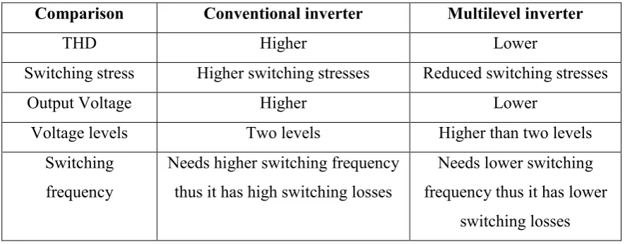
The comparison between conventional and multilevel inverter is shown in Table 1.1 below. The main difference that distinct multilevel inverter from conventional inverter is that it produces output with lower total harmonic distortion. This will lead to lower switching stresses in the inverter circuit and thus lower switching losses. Besides, output voltage of multilevel inverter is higher since the output voltage of it is equal to the summation of each H- Bridge cell’s output voltage. Multilevel inverters have more than two output voltage levels while conventional inverters have two voltage levels. For multilevel inverters, they need lower switching frequency compared to the conventional inverters to produce the desired output waveform. Therefore, the switching losses are lower than that of the conventional inverter. The power supply can be used to perform other useful task.
3
Table 1.1: Comparisons between conventional inverters and multilevel inverters Comparison Conventional inverter Multilevel inverter
THD Higher Lower
Switching stress Higher switching stresses Reduced switching stresses
Output Voltage Higher Lower
Voltage levels Two levels Higher than two levels
Switching frequency
Needs higher switching frequency thus it has high switching losses
Needs lower switching frequency thus it has lower
switching losses
1.3 Problem Statement
4
1.4 Objective
There are four objectives in this paper.
First, this project aims to investigate on types of inverter and to simulate it using MATLAB Simulink.
Second, the objective of this project is to simplify the switching strategy for multilevel inverter.
Third, this project aims to implement a voltage based SPWM technique for 5- Level Cascaded H- Bridge Multilevel Inverter.
Fourth, this project aims to analyse the multilevel inverter performance in terms of total harmonic distortion (THD) and the power factor.
1.5 Scope
The scopes of this project are:
1. This project will focus on the single phase 5- level cascaded H- bridge multilevel voltage source inverter.
2. The input DC voltage for the inverter is 60V; the peak voltage of the output sine waveform is 120V before adding filtering circuit.
3. A voltage based SPWM technique is implemented using modified PID controller.
5
CHAPTER 2
LITERATURE REVIEW
2.1 Introduction
Inverters are power electronic converters that convert direct current (DC) source into alternating current (AC) output. Since trend of industrials nowadays require higher output power, thus multilevel inverters are introduced. There are several types of multilevel inverters which are implemented by several techniques.
In this chapter, types of multilevel inverters and Pulse Width Modulation (PWM) techniques will be discussed.
2.2 Topologies of Multilevel Inverter
There are three common topologies of multilevel inverter which are: i. Cascaded H- Bridge
ii. Flying Capacitors iii. Diode- clamped
Thongprasri (2011) had tabulated the numbers of components needed by different types of multilevel inverters as in Table 2.1 below. Cascaded H-bridge inverter is the topology that requires least number of components.
6
Table 2.1: Components of Single Phase Multilevel Inverters[4] Types of multilevel
inverter
No. of switches No. of diodes No. of capacitors
Cascaded H- bridge 8 - -
Flying capacitors 8 - 10
Diode- clamped 8 12 4
2.2.1 Cascaded H- Bridge
Cascaded H- Bridge Multilevel Inverter is popular topologies among all multilevel and multi- pulse inverters. This is due to the structures of H- bridges in a multilevel inverter are identical and it enables the H- bridge to be modularized, manufactured and packaged easily [5]. Low switching frequency and the ability to be modularized are the advantages of cascaded H-bridge inverter. There are some cons when using Cascaded H- Bridge topology too. When the output voltage level increases, the switches and dc sources have to be increased, which leads to increasing cost and weight of the circuit[6]. The levels of output voltages can be increased by two levels by cascading an H- bridge module to the existing one. The number of output voltage levels can be calculated using the formula, 2m+1; where m is the number of cells as shown in Figure 2.1. The idea of this inverter is connecting H-bridge inverters serially to get a sinusoidal output voltage. The output voltage can be calculated by summing the voltage produced by each H- Bridge. It needs fewer components compared to diode-clamped and flying capacitors type multilevel inverters.
[image:20.595.212.394.532.735.2]7
2.2.2 Diode- Clamped
[image:21.595.125.490.359.665.2]The Diode- Clamped Multilevel Inverter topology was proposed in 1981. This topology as shown in Figure 2.2 is also known as neutral point inverters and it is designed for low frequency applications [7]. The number of components needed in this topology depends on the number of output voltage levels desired. (n-1) voltage source, 2(n-1) switching device and [(n-1) (n-2)] diodes are needed for n level inverter; given n is the number of output voltage levels as stated by Varsha and Shraddha (2013). This inverter’s idea is by using diodes, it limits bus voltage to reach the require steps in the output [8]. The advantage of using diode- clamped topology is that all phases using the common bus for its application in three phases. The disadvantage of using this topology is the difficulty faced in real power flow. This is due to the imbalanced capacitors and it made this topology less popular in industries.
8
2.2.3 Flying Capacitors Clamped Multilevel Inverter
[image:22.595.107.501.274.597.2]Flying Capacitors Clamped was proposed by Maynard and Foch in 1992 [9]. As stated by Ahmed (2014), the topologies of Flying Capacitors Clamped and Diode Clamped Multilevel Inverter are almost the same except that capacitors are used in Flying Capacitors Clamped topology and diodes are used in Diode Clamped topology. This topology needs the largest number of capacitors compared to Cascaded H- Bridge and Diode Clamped topologies to limit the output voltage to a certain level. Practically, this topology can produces only six levels output voltage although theoretically it can gives infinite levels. The arrangement of capacitors, switches and diodes is shown in Figure 2.3.
Figure 2.3: Flying Capacitors Clamped 5- Level Inverter Topology
2.3 Sinusoidal Pulse width modulation (SPWM)
9
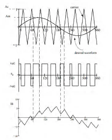
[image:23.595.122.487.134.590.2]a lower frequency modulating sine-wave signal and the higher frequency carrier triangular signal. A simple voltage based inverter is shown in Figure 2.4.
Figure 2.4: Principle of PWM
2.3.1 Sinusoidal Pulse Width Modulation for Multilevel Inverter
10
[image:24.595.202.416.174.348.2]used to generate the desired output voltage. In certain condition, the switch will be switched ON or OFF depending on whether positive or negative dc bus voltage is applied at the output. In phase disposition where the carriers are shifted vertically as shown in Figure 2.5, all four carriers are at the same frequency, phase and amplitude. The comparison between the reference signal and the four carrier signals is performed.
Figure 2.5: Carriers which are shifted vertically [6].
2.4 PID Controller
PID controller is a controller that get output value by reading a sensor, then control the output actuator to produce desired output by computing proportional, integral, and derivative responses. Figure 2.6 shows the position of a PID controller in a control system; while Figure 2.7 shows the block diagrams inside a PID controller.
In PID controller, there are three main components which are Proportional (P), Integral (I) and Derivative (D). The P component in PID controller multiply the error signal by the Proportional gain (Kp), I component is the sum of all the instantaneous error signal and D component functions as a future- predicting component. D component does the control action by calculating the future measured value and projecting the current measured value. However, D component will affect the output where it will cause noises. Therefore, the Derivative gain (KD) must not be too large.
![Table 2.1: Components of Single Phase Multilevel Inverters[4]](https://thumb-us.123doks.com/thumbv2/123dok_us/73278.6893/20.595.212.394.532.735/table-components-single-phase-multilevel-inverters.webp)
![Figure 2.2: Diode- Clamped 5- Level Inverter Topology[7]](https://thumb-us.123doks.com/thumbv2/123dok_us/73278.6893/21.595.125.490.359.665/figure-diode-clamped-level-inverter-topology.webp)

![Figure 2.5: Carriers which are shifted vertically [6].](https://thumb-us.123doks.com/thumbv2/123dok_us/73278.6893/24.595.202.416.174.348/figure-carriers-shifted-vertically.webp)