Modeling of Photovoltaic Grid Connected
Generation System Based on Three Level NPC
Converter
Francisco Javier Arcos-Pardo, Jos´e Luis Monroy-Morales,
M´aximo Hern´andez- ´
Angeles
Programa de Graduados e Investigaci´on en Ingenier´ıa El´ectrica Instituto Tecnol´ogico de Morelia
Morelia, Michoac´an M´exico
Email:fcojarcospardo@ieee.org, jlmonroy m@itmorelia.edu.mx, mhernand it@yahoo.com.mx
David Campos-Gaona
Wind Energy and Control CentreUniversity of Strathclyde 99 George St, Glasgow G1 1RD, UK
Email: davidcg@ieee.org
Abstract—Renewable energy sources have been increasing and developing continuously in the last years, due to advantages over conventional generation sources. Photovoltaic (PV) systems gen-erate electricity from sunlight without creating any air or water pollution and in a clean, quiet and reliable way. The efficiency and performance of PV systems are still under development. As a consequence, the control structures of the PV system grid-connected are a fundamental part for its proper functioning. In this paper, a grid connected photovoltaic system based on a three-phase three-level neutral point clamped (NPC) inverter is presented. The proposed system describes in detail each stage along with the suited controllers, which operate in a proper and efficient way. In addition, the Perturbation and Observation (P&O) algorithm to get the maximum power point tracking (MPPT) of the PV system under different irradiation conditions, is proposed. In order to maximize the PV system power, a three-phase three-level NPC converter is used to achieve higher power levels, lower voltage stress on devices, lower switching frequency and reduce harmonic content. In addition,d-qreference frames are used to decouple the active and reactive power controllers. Simulations to validate the proposed procedures of the complete system are presented.
I. INTRODUCTION
The harmful effects caused by conventional power sources on the planet and the increasing energy demand have lead to the use of the natural resources as an alternative for energy production. [1]. Recently, the use of renewable energy sources have increased in order to solve the issues of growing energy consumption, the finite nature of fossil fuels and the worsening of the global environment [2]. Solar photovoltaic systems are widely known for the ability to generate electric power from the sunlight, and offer generated electricity in a clean, quiet and reliable way. Therefore, PV generation systems have been enhanced and considered as one of the most developed in power generation. These systems can work either in stand alone or grid connected mode.
The grid connected photovoltaic system has been widely implemented in electrical networks, however it is prone to
affect the power quality of electrical networks by producing voltage sags, flicker, and harmonics. Also, solar energy is in-termittent in nature and the power output from the PV modules changes with temperature and radiation levels. Therefore, the PV system controllers approaches must be able to solve the grid integration problems and extract the maximum power from PV generators under any weather conditions.
The voltage source inverters are an important component for renewable energy sources. Multilevel inverters are used in high-power and medium-voltage applications due to their competitive advantages over their two levels counterparts. Some of their advantages are, e.g., reduced switching-voltage ratings, smaller switching stresses dv/dt, an improved output voltage at lower switching frequencies and reduce harmonic currents generated by the inverter using an appropriate selec-tion of switching vectors [3]. These characteristics have led to the development of many applications including PV systems where the multilevel topology allows to generate a wide range of output voltage levels [4]. Since the photovoltaic voltage output is a DC voltage, a DC-DC converter is used in order to shape the inverter voltage input and take advantage of a higher energy production. In addition, a MPPT (Maximum Power Point Tracking) controller is required to detect the PV system maximum power point tracking.
In this paper, a complete three-phase three-level NPC inverter grid-connected photovoltaic system, as shown in Fig. 1, is presented. The active and reactive power is controlled in accurate and appropriate way by mean of a NPC three-level inverter in order to take advantages over conventional topologies. The mathematical model for grid-connection are described in a detailed manner.
II. PHOTOVOLTAIC PANEL CONDITIONING
Connecting several solar cells in series or parallel is carried out in order to get proper power levels [5]. The PV systems drawbacks is that the solar radiation falling upon solar panels is not constant. The variation depends on many factors, e.g.,
Sunlight
PV arrangement
Electrical network synchronization DC-DC
Converter
DC-AC
Converter Grid
[image:2.612.72.271.49.130.2]MPPT
Fig. 1. PV system complete block diagram.
the area weather conditions where the PV is installed, which causes over-voltages or voltage and current drops. Therefore, a variable DC signal is closer to a real electrical signal generated by the sunlight, as shown in Fig.2. A variable
160 140 120 100 80 60 40 20
0 0.002 0.004 0.006 0.008 0.012 0.014 0.016 0.018 Time (s)
DC VOLTAGE SIGNAL ( V )
[image:2.612.350.520.174.286.2]0.01
Fig. 2. DC signal conditioning.
DC signal enables having a quasi-realistic PV real behavior, plus the inclusion of sharp voltage level variations as sudden changes of elevations and falls in voltage can be represented as step response. In order to obtain the desired behaviors in the generated CD components, an arrangement of signals in time can be implemented as shown in Fig. 3. The generated and manageable signal must be transformed into a electrical signal through a simulation component.
X
Generator signals
Magnitude
[image:2.612.75.271.230.363.2]Transducer: time signal to electrical signal
Fig. 3. Simulation diagram for the generated DC signal.
In Fig. 3, the magnitude block is a constant signal used to modify the amplitude of the generated signal. The generator signals block is programmed to obtain a desired waveform as shown in Fig. 2. A transducer is used to convert the generated signal into a electrical signal. The model presented in Fig. 3 is different from those previously studied where the PV panel is modeled based on solar cells maths equations [6]. However, the model presented in Fig. 3 allows analyze diverse and specific waveforms, including both those closer to real signals and the considered “hard testings”. In this way, the complete system robustness is proved.
III. DC-DC CONVERTERCONTROLLER
In PV systems, a DC-DC converter is commonly used between the PV panel output and the inverter input. The DC-DC converter purpose is to adjust the voltage levels to feed the inverter. The Boost converter is useful for PV systems applications to obtain a better exploitation of the generated energy. The Boost converter is able to increase a Vs output
voltage fromVininput voltage.
Fig. 4 shows the Boost converter topology. A DC-DC
con-Vs Is
Qs
L D
RL
C
Ic Io
ID
I
Fig. 4. Boost converter circuit.
verter adjusts the relationship Vin/Vs by mean of a control
variable namedduty cycle(D),
D= 1−Vin
Vs
(1)
A MPPT algorithm is used to control the DC-DC converter duty cycle. The MPPT is the PV panel optimal operating point where the generated energy has the highest possible benefit [7]. The Boost converter control block diagram is shown in Fig. 5.
There are several methods to obtain the MPPT. Advanced
PWM Generator v
p , ip D
MPPT Boost
[image:2.612.359.528.435.470.2]converter
Fig. 5. Buck converter block diagram.
control algorithms are based on the P&O method since pro-vides a fast and efficient control solution [8]. Therefore, the P&O algorithm is implemented in this paper, and is shown in Fig. 6.
The P&O algorithm compare the panel voltage and current with the immediately previous value of power to detect changes and adjust the duty cycle in an suitable way. Thus, a converter regulated signal output, by mean of a proper pulse wide modulation, is achieved.
IV. NPC THREE-LEVEL INVERTER
A three-phase three-level NPC inverter is shown in Figure 7. Each phase share a common DC bus, subdivided by two capacitors in three levels. The voltage across each capacitor is VDC/2; and the voltage stresses across each
switching device and clamping diodes are limited toVDC/2.
[image:2.612.74.272.483.547.2]V(k) and I(k) Measurement
P(k) = V(k)*I(k) ∆P= P(k) - P(k-1)
Not Yes
∆P>0
V(k) - V(k-1)>0 V(k) - V(k-1)>0
Not Not
Yes Yes
Decrease Duty Cycle Decrease
Duty Cycle
Increase Duty Cycle
Increase Duty Cycle
Update Values V(k-1) = V (k) P (k-1) = P(k)
P&O Algorithm
Fig. 6. P&O algorithm.
inverter reduces harmonics in both, current and voltage output.
T1a
T2a
T3a
T4a
D1a
D2a
D1b
D2b
D1c
D2c
T3b
T2b
T1b
T4b T4c
T3c
T2c
T1c
N V
DC
2
V
DC
2 V
DC
Ia
V
sa Vsb Vsc
[image:3.612.67.279.50.259.2]Ib Ic
Fig. 7. Three-level NPC inverter topology.
Table I shows the switch states for phase a, and similar switching sequences can be derived for the remaining phases considering a displacement of 120◦. Here, T1a and T3a are
complementary between them and so on for T2a and T4a.
State condition 1/0 means switch ON/OFF conditions. In
TABLE I
SWITCHINGSTATES FOR ATHREE-LEVELNPC INVERTER
States of switches Voltage T1a T2a T3a T4a Level
VaN
1 1 0 0 +VDC/2
0 1 1 0 0
0 0 1 1 −VDC/2
Fig. 8 a detailed NPC inverter operation is shown. For phase a, three possibles switching states are required to have the three desired levels. Similar operation is for phases B andC
taking in account the 120◦ shifted.
The output voltage, Vk
s, can be calculated as,
Vsk =VDC−
nk−1
X
i=1
VTk
i (2)
wherenis the number of levels of the converter and kstand for the phases a, b and c. VDC is the converter DC input
voltage andVTk
i is the switching devices voltage drop,
VTk
i = (1−T
k
i)VCi (3)
T ik is corresponding to onor off switching device state, and
VCiis the capacitors voltage connected in series.
Substituting equation (3) in equation (2), the output voltage from the switching signals is,
Vsk =
nk−1
X
i=1
TikVCi (4)
The NPC optimal performance depends mainly of the
vaN
VDC
VDC/2
VDC/2
VDC/2
VDC/2
VDC/2
VDC/2
D1a
D2a
N
T1a T
1b
T
2b
T
3b
T4b
T1c
T2c
T3c
T4c
T2a
T3a
T
4a
a
vaN
VDC
D1b
D2b
N a
vaN
VDC
D1c
D2c
[image:3.612.322.549.319.480.2]N a
Fig. 8. Three-level NPC switching states, output voltages.
[image:3.612.81.269.340.460.2]0.6
0.4
0.2
0
-0.2
-0.4
-0.6
-0.8
0 0.002 0.004 0.006 0.008 0.01 0.012 0.014 0.016 0.018
Time (s)
Moduladora Portadora 1
0.01
[image:4.612.59.287.68.167.2]Portadora 2
Fig. 9. Phase Disposition technique for three-level converter.
V. GRID CONNECTEDPV SYSTEM
The inverter grid-connected diagram is shown in Fig. 10. The grid voltages and currents are become into DC signals by mean of d-q transformation under balanced sinusoidal conditions and perfect synchronization [10]. The grid and inverter voltages are synchronized employing a phase-locked loop (PLL). Considering the inverter is connected to the grid,
abc
dq abc
dq
abc dq
PLL
PWM
KP + KI/S
WL
-WL
KP + KI/S
+ +
++ +
-+ -+
+ ++
GRID +
-ea
ec
eb
VDC
iaibic
Vc Vb Va
Vq Vd
Id Iq
Id Id
Iq
Iq
eq
ed
Vd
Vq
[image:4.612.56.285.307.526.2]Three-phase Three-level inverter
Fig. 10. Overall diagram of grid-connected converter control.
voltages and currents are defined as,
vx=Rix+L
dix
dt +vxinv (5)
wherex= a, b and c.
vx and ix are ac grid voltages and currents respectively and
vxinv is the three-level inverter voltage. The three-level inverter
is connected to the grid by mean of the resistance R and the inductance L. The abc to d-q transformation is applied to (5) and now the voltages and currents are expressed in two references frames, d-q, synchronously rotating at AC frequency, wcopl, as shown in (6) and (7).
vd=Rid+L
did
dt −wcoplLiq+vd−inv (6)
vq =Riq+L
diq
dt +wcoplLid+vq−inv (7)
The d and q subscripts stand for the direct and quadrature axis, respectively.
Ecuations (6) and (7) have induced terms wcoplLid and
wcoplLiq that gives cross-coupling between the two axes.
These cross-coupling terms can be taken as disturbances from control point view.
The power exchange ind-qreference frame is given by,
P= 3
2(vdid+vqiq) =vdcidc (8)
where vdc and idc are DC outputs voltages and currents.
Equation (8) represents the power balance ratio between the ACinput and theCDoutput. On the DCside,
idc=C
dvCD
dt +iL (9)
In equation (8), the grid voltage vector can be defined to be along thed-axis direction,vq = 0. Therefore, the instantaneous
real and reactive power can be calculated as,
p=3
2vdid (10)
q=−3
2vdiq (11)
As can be seen in equations (10) and (11), the active and reactive power are controlled by the id and iq currents
respectively. The PV system inverter control is carry out considering two PI control loops in cascade, a dc voltage controller providing reference signals to the control system and the current controller that generates the switching signals according to the reference and measured signals [11].
A. Current Controller
The current controller block diagram is shown in Fig. 11
V’inv V
inv
I
d Iq
I
d_ref Iq_ref
-+ PI
Controller
PWM Converter
System Transfer Function
Fig. 11. Current controller block diagram.
Inside the PI controller block, there are twoPI regulators, for thedandqaxis current, respectively. After comparison, these PIcontrollers transform the error between thedandqcurrent components into voltage magnitudes.
Equations (6) and (7) have a similar form, so that, only the d-axis equations are used for further analysis. Consequently theq-axis controller will also have the same parameters. From Fig. 11, the equation for theP I regulator is,
{idref(s)−id(s)}
Kp+
Ki
s
[image:4.612.326.549.519.565.2]
whereKp andKi are the proportional and integral constants
for current control.
The PWM converter block can be considered as an ideal power transformer with a time delay equal to half the switching cycle and produced by the inverter switches. Thus the PWM block is given as,
Y(s) = 1
1 +Tas
(13)
whereTa=Tswitch/2.
The controller system have the reference signal and the feed forward signals in order to eliminate the cross coupling terms. Thus, the inverter voltage using these inputs are defined as,
v0d inv=−(id ref−id)
Kp+
Ki
s
+wcoplLiq+vd (14)
Using the previous equations and Laplace transformation, the system transfer function is,
G(s) =
1
R+Ls
(15)
The modulus optimummethod are used for tuning the current controller, this method is widely used because of simplicity and fast response.
B. Voltage Controller
The voltage controller general block diagram is shown in Fig. 12. The voltage controller is composed by PI voltage controller, current controller and the system transfer function where the capacitor is the principal element.
Id_ref Current Id Vdc
Controller Vdc_ref
-+
PI Controller
Current controller
System Transfer Function
(
Tiv s
Kpv
(
1+Tiv s 1
s C
Current controller
Fig. 12. General block diagram ofvdccontroller.
For the PI controller in the Laplace domain, is:
{Vdc ref(s)−Vdc(s)}
Kpv+
Kiv
s
=id ref(s). (16)
The subscript “v” denotes the voltage regulator.
The simplification of the second order transfer function of the current controller, by equivalent first order transfer function can be approximated as
W(s) = 1
Teqs+ 1
(17)
whereTeq= 2Ta.
AssumingVq= 0in equation (8), the relationship betweenid
andIdcis,
Idc=
3
2
Vd
Vdc
id. (18)
Equation (18) defines the current gain value. Therefore, the voltage controller controls the capacitor current so as to maintain the power balance.
The overall control block diagram of thedcvoltage controller is as shown in Fig. 13. For tuning the voltage controller, the
Current Loop
Vdc_ref Vdc
-+ +-
(
Teq s+1(
+-1 3Vd
2Vdc
1 s C
Id Idc IC
IL
Id_ref
2Vdc 3Vd
[image:5.612.330.540.122.191.2](
Tiv s Kpv(
1+Tiv sFig. 13. Closed loop control diagram ofdcvoltage controller.
symmetrical optimummethod are used.
VI. SIMULATION RESULTS
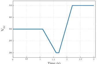
In order to verify the system performance, simulations based on Fig.1 were carried out. A varying-time DC signal which can closest describe the PV behaviour is shown in Fig. 14. As shown in this figure, the DC voltage value is 300v with
±10VDC variations.
0 0.5 1 1.5 2 2.5 3 290
295 300 305 310
Time (s)
VD
[image:5.612.345.513.334.446.2]C
Fig. 14. Generated input voltage supplied to grid-connected system.
As can seen from Fig. 1, the PV panel is fed for a signal as that shown in Fig. 14. As mention before, solar energy is intermittent in nature and the power output from the PV modules changes with the radiation levels. Consequently, the simulation ofDC-DC converter output voltage when a MPPT algorithm is not considered was carried out and is shown en Fig. 15. Due to the above, a DC-DC boost converter is required to regulate the DC voltage applied to the inverter.
The photovoltaic voltage variations leads to no proper behaviour in the dc-dc converter when no control in duty cycle is performed. Therefore, the DC-DC converter duty cycle must be controlled by a MPPT algorithm, otherwise, the DC-DC converter output will have voltage and current variations originated by solar irradiation. The regulated DC output voltage using theP&O MPPT algorithm is shown in Fig. 16. The boost converter raises from 300VCDto 500VCD.
0 0.1 0.2 0.3 0.4 0.5 0.6 0.7 0.8 0.9 1 0
50 100 150 200 250 300 350 400 450 500
Time (s)
VD
[image:6.612.91.249.56.170.2]C
Fig. 15. Boost converter output voltage without MPPT control.
0 0.5 1 1.5 2 2.5 3
0 100 200 300 400 500 600
Time (s)
VD
[image:6.612.87.252.204.317.2]C
Fig. 16. Boost converter output voltage controlled by MPPT.
references, respectively. In Fig. 17, the measured and reference active power are shown when the reference value changes in three different values, P= 800w, P= 1,200w and P= 1,000w. In the same way, different changes in the reference reactive power are simulated as shown in Fig. 18. In this figure, the measured reactive power tracks the reference reactive power value in Q=100, Q=-100 and Q=0, which is the desired value for system. As seen in Figs. 17 and 18, the used controller allows the reference active and reactive power proper tracking. Important to mention that the maximum active power injected to the grid depends on the panel photovoltaic capabilities.
0 1 2 3 4 5 6 7 8 9
600 800 1000 1200 1400
Time (s)
P (Watts)
P MEASURED P REFERENCE
P=800
P=1200
P=1000
Fig. 17. Boost converter output voltage controlled by MPPT.
Time (s)
0 1 2 3 4 5 6 7 8 9 10
Q (Vars)
-150 -100 0 100 150
Q MEASURED Q REFERENCE
Q= -100
Q= 0 Q=100
Fig. 18. Boost converter output voltage controlled by MPPT
VII. CONCLUSIONS
A grid connected PV system is a viable solution provide energy from renewable sources. These systems generate elec-tricity from sunlight without pollution. This paper describes all the elements of a grid connected PV system. The DC-DC converter along with MPPT algorithm leads to have regulated voltage and therefore an NPC inverter appropriate performance.
In addition, the used NPC topology, allows handle higher power. For active and reactive power control, thed-qreference frames are applied to provide a decoupled control. Moreover, power electronics has proved the possibility to implement a PV systems because of high switching device development. Simulations results have proved the good performance of the proposed system along with the controllers rules.
REFERENCES
[1] H. Reham, AEI Aroudi, ACid-Pastor, G. Gar’lca, C. Olalla and L. Salamero,Impedance Matching in Photovoltaic Systems Using Cascaded
Boost Converters and Sliding-Mode Control, IEEE Transactions on power
electronics, Vol. 30, No. 6, June 2015.
[2] M. Dali, D. Belhadj and X. Roboam, Hybrid solar-wind system with battery storage operating in grid–connected and standalone mode:
Con-trol and energy management-experimental investigation,Energy, vol. 35,
2010, pp. 2587–2595.
[3] Jos´e Luis Monroy-Morales, David Campos-Gaona, M´aximo Hern´andez-´
Angeles, Rafael Pe˜na-Alzola and Jos´e Leonardo Guardado-Zavala, An Active Power Filter Based on a Three-Level Inverter and 3D-SVPWM for
Selective Harmonic and Reactive Compensation, Control and
Commu-nication in Distributed Generation Systems, Energies 2017, 10(3), 297; doi:10.3390/en10030297.
[4] Goetz, S.; Zhongxi, L.; Liang, X.; Zhang, C.; Lukic, M.; Peterchev, A.V., Control of modular multilevel converter with parallel
connectiv-ity—Application to battery system. IEEE Trans. Power Electron. 2016,
doi:10.1109/TPEL.2016.2645884.
[5] Roger A. Messenger and Jerry. Ventre,Phtovoltaic Systems Engineering, 2nd ed. Florida, USA: CRC PRESS, 2005.
[6] Gow, J. A. and Manning,Development of photovoltaic array model for
use in power electronics studies, IEE Proceedings on electric power
applications, 1999.
[7] R. Sridhar and N. Thamizh Selvan and S. Jeevananthan and P. Sujith Chowdary, Performance improvement of a photo voltaic array using
MPPT (P&O) technique, INTERNATIONAL CONFERENCE ON
COMMUNICATION CONTROL AND COMPUTING TECHNOLO-GIES, 2010.
[8] William Christopher and R. Ramesh,Comparative Study of P&O and InC
MPPT Algorithms, American Journal of Engineering Research (AJER),
2013.
[9] Ilhami Colak and Ersan Kabalci and Ramazan Bayindir,Review of
multi-level voltage source inverter topologies and control schemes, Elsevier,
2010.
[10] F. N. Gakis, S. A. Papathanassiou, “Simple control schemes for grid-connected three-phase voltage-source inverters of DG units”, Proc.XVII International Conference on Electrical Machines, ICEM’2006, 2-5Sept.2006 Chania, Greece.
[image:6.612.89.251.500.582.2] [image:6.612.91.252.623.704.2]