City, University of London Institutional Repository
Citation
: Ghosh, S. & Rahman, B. M. (2018). Evolution of Plasmonic Modes in a Metal
Nano-Wire Studied by a Modified Finite Element Method. Journal of Lightwave Technology,
36(3), pp. 809-818. doi: 10.1109/JLT.2017.2782710
This is the accepted version of the paper.
This version of the publication may differ from the final published
version.
Permanent repository link:
http://openaccess.city.ac.uk/19876/
Link to published version
: http://dx.doi.org/10.1109/JLT.2017.2782710
Copyright and reuse:
City Research Online aims to make research
outputs of City, University of London available to a wider audience.
Copyright and Moral Rights remain with the author(s) and/or copyright
holders. URLs from City Research Online may be freely distributed and
linked to.
Abstract— A finite width thin metal film plasmonic nanowire with its unique feature of sub-wavelength light guiding is finding many applications in compact integrated nanophotonic circuits and sensors. Full-vectorial finite element method (FV-FEM) is becoming an important simulation tool for the analyses of such exotic waveguides. Instead of a penalty approach reported earlier, a more direct divergence formulation considering each discretized element’s optical properties to eliminate non-physical modal eigenvectors has been exploited and is reported here. Long and short-range fundamental and higher order plasmonic modes and supermodes of a pure metal nanowire and their evolutions with waveguide geometry, surrounding identical and non-identical dielectric cladding materials and operating wavelength are thoroughly studied. Interesting long-range modal properties such as, supermode formation, complex phase matching and mode evolution in identical and non-identical clad metal nanowires have been observed and explained in detail including supermode profiles. This study is expected to help in understanding the evolution of plasmonic guided modes in compact active and passive integrated photonic devices containing metal narrow strips.
Index Terms— Computational electromagnetic methods, Finite
element method, Surface plasmon, Plasmonics, Waveguides.
I. INTRODUCTION
ntegration of photonic devices and nano-electronics are challenging due to ingrained diffraction limit of electromagnetic energy supported by dielectric media. The surface plasmon polaritons (SPPs) can be one of the solutions to overcome this difficulty. Comparing with other nano-scale waveguides, such as, high-index contrast silicon-on-insulator (SOI) nano-wires and photonic crystals (PCs), surface plasmon (SP) shows a true nano-scale light guiding. The light guiding characteristics of conventional dielectric waveguides and pure plasmonic waveguides are opposite in nature. A
This work was supported in part by City, University of London and in part by Erasmus Mundus AREAS+ Ph.D. fellowship and SPIE Optics and Photonics Education Scholarship program for Ph.D. and research funding.
The authors are with the Department of School of Mathematics, Computer Science and Engineering, City, University of London, London EC1V 0HB, U.K. (e-mail: [email protected]; [email protected] ).
high-index contrast SOI nano-wire confines light in the high index region with a relatively low propagation loss and hundred nanometer size mode area are also key properties of these structures [1], [2]. However, a pure metal plasmonic waveguide although provides a more compact light guiding but often with a very higher propagation loss [3]. In case of a plasmonic nano-guide, where its width is comparable to its height, plasmonic mode also forms along their vertical interfaces and combined with the plasmonic modes at the horizontal interfaces. Their phase matching and evolutions are more complex. This in turn requires a methodical investigation of pure plasmonic modal properties to design the compact long-range plasmonic and hybrid plasmonic waveguides [4], [5] of the future to exploit the unique features of SPPs in the applications of nano-dimensional passive waveguides, devices [6], [7], and for bio-chemical [8] and gas sensing [9].
The SPP denotes a surface propagating electromagnetic wave which shows a sub-wavelength energy confinement at the conducting metal and dielectric interface. The complimentary optical properties of noble metals and dielectrics at the interface in visible and near infra-red (NIR) region helps to excite the SP waves. These modal fields show a strong spatial variations and tight confinement at the interface and decays exponentially away from this interface. In case of a thin metal film bounded by dielectrics, two interface modes come closer and couple to form plasmonic supermodes (PSM). Due to ohmic loss in the metals these SPP modes have short propagation length. The pure plasmonic modes are transverse magnetic (TM) polarized and evanescently confined in the direction normal to the propagation. In this work, we have considered the widely-used telecommunication wavelength 1550 nm for SPP modal excitations.
The design and application of plasmonic and hybrid plasmonic waveguides require a clear knowledge of the basic SPP modes and their characteristics and evolution with the waveguide geometry, surrounding materials and operating wavelength variations. Thus, the plasmonic modal investigation of a thin metal film with finite width is important. To accomplish this objective a numerically efficient and accurate divergence modified H-field based full-vectorial finite element method (FV-FEM) is presented and used as a simulation tool for modal analyses.
Evolution of Plasmonic Modes in a Metal
Nano-wire Studied by a Modified Finite Element
Method
Souvik Ghosh,
Student Member, IEEE
and B. M. A. Rahman,
Fellow, IEEE
II. THEORY
For the accurate characterization of a SPP based waveguide requires an exact calculation of the complex modal propagation constant (𝛽), effective indices (𝑁𝑒𝑓𝑓), effective
area (𝐴𝑒𝑓𝑓) and full-vectorial dominant and non-dominant
field profiles of various modes. All these parameters can be determined by solving the Maxwell's equations with appropriate boundary conditions for the waveguide. For a complex structured waveguide with isotropic or anisotropic media, an analytical or semi-analytical approach exhibits mathematical difficulties. A full-vectorial H-field based finite element method shows the potential to characterize the arbitrary shaped waveguide problems.
A. Divergence Modified Full Vector Finite Element Method
In 1956, Berk [10] suggested several approaches to formulate the electromagnetic (EM) fields into a variational form. However, the H-field based formulation is the most favorable than the others (E-field, E+H-field and 𝐸𝑧+ 𝐻𝑧) as
the H-field for optical waveguides is naturally continuous at the dielectric boundaries [11]. In this report, we have modified our in-house FV-FEM code based on the H-field based formulation to implement divergence condition for plasmonic waveguides. Following the minimum theorem, the initial variation of the functional 𝐹 based on Maxwell’s curl equations must be zero, 𝛿𝐹 = 0. This actually proves the stationarity of the functional by minimizing the energy associated with the functional.
𝐹 = 〈𝜖̂𝑟−1(∇×𝑯), (∇×𝑯)〉 − 𝜔2〈𝜇̂𝑯, 𝑯〉 (1)
Here the parameters 𝜔, 𝜖̂ and 𝜇̂ are the angular frequency (𝜔2 being the eigenvalue), permittivity and permeability
tensors, respectively. The braces in Eq. 1 indicates the inner product with the equation form of 〈𝑨, 𝑩〉 = ∬ 𝑩∗⋅ 𝑨 𝑑𝑥𝑑𝑦.
The Euler form of the above equation satisfies the Helmholtz's equation but unfortunately that does not obey the Maxwell's two divergence equations and thus can generates unwanted spurious solutions along with the true physical solutions. Earlier, Rahman and Davies proposed a successful way of removing spurious solution by balancing the curl and divergence part with a penalty function method [12]. A global weighting factor close to the value of 1/𝑛𝑒𝑓𝑓2 was used to
incorporate the effect of divergence equation (𝑑𝑖𝑣 ⋅ 𝑩 = 0). This method has been very efficient to determine the accurate solution of a wide range of passive dielectric based waveguides, particularly with all positive dielectric constants but has been less effective for plasmonic waveguides where the SPs are guided by metals or composite structure of dielectrics and metals. Here, a more direct approach is proposed where, the contributions of both positive and negative permittivities of local materials are considered into additional divergence-divergence part. During formation of the global matrices of the curl-curl and divergence-divergence sections individual local dielectric constant of the discretized triangular element is considered. We finally obtain the
modified form of the functional with additional divergence-divergence inner product as
𝐹𝑒= 〈𝜖̂𝑟−1(∇×𝑯), (∇×𝑯)〉 + 〈𝜖̂𝑟−1(∇ ⋅ 𝑯), (∇ ⋅ 𝑯)〉
− 𝜔2〈𝜇
𝑟
̂𝑯, 𝑯〉 (2)
Here 𝐹𝑒 denotes the standard variational functional for a
single element. For 2D modal solutions, the field time dependence 𝑒𝑗𝜔𝑡 is assumed throughout and for a waveguide
the z-dependency in the direction of propagation is taken as 𝑒−𝑗𝛽𝑧. In case of three-dimensional electromagnetic
waveguide and resonator problems the modal fields are distributed in all three directions. Thus, the same variational formulation can be used for a resonator problem without considering the wave propagation assumption [13]. It is also notable that the Euler equation of the modified functional (𝐹𝑒)
satisfy Maxwell's both curl and divergence equations. Finally, following minimum theorem (𝛿𝐹 = 0) and integral form of the inner product we obtain a compact standard and stationary eigenvalue equation.
𝜔2= ∬ [(∇×𝑯)∗⋅ 𝜖
𝑟
̂−1(∇×𝑯) + (∇ ⋅ 𝑯)∗𝜖
𝑟
̂−1(∇ ⋅ 𝑯)]𝑑𝑥𝑑𝑦
/∬ 𝑯∗𝜇
𝑟
̂. 𝑯 𝑑𝑥𝑑𝑦 (3)
The solution of Eq. 3 provides the eigenvalues and associated eigenvectors. The modal propagation constant and effective indices (𝑁𝑒𝑓𝑓 = 𝑛𝑒𝑓𝑓 + j𝑘𝑒𝑓𝑓) can be calculated from
the eigenvalues whereas, the associated eigenvectors represent the modal field distributions.
Plasmonic waveguide modelling also requires accurate determination of modal power attenuation (𝛼) and propagation length (𝐿𝑝). The propagation length (𝐿𝑝) defines the
waveguide length where mode power drops to 1/𝑒 of its initial value and this can be given as, 𝐿𝑝 = 𝜆/4𝜋𝑘𝑒𝑓𝑓. Additionally,
the modal attenuation (𝛼) can be obtained from, 𝛼 = 4.343/𝐿𝑝.
The light confined by the waveguide and surrounding media is determined by the modal effective area (MEA). As the E and H field profiles in a plasmonic mode have significantly different mode field profiles, we have followed the mode effective area calculation that included the z-component of
modal Poynting vector (𝑆𝑧 = 1 2(𝑬×𝑯
∗) ⋅ 𝑧̂), which considers
the effect of both E and H fields:
𝑀𝐸𝐴 = (∬ 𝑆𝑧 𝑑𝑥𝑑𝑦) 2
∬ 𝑆𝑧2 𝑑𝑥𝑑𝑦
⁄ (4)
III. MODAL CHARACTERISTICS OF METAL NANOWIRE
We study a silver (Ag) nanowire of finite width embedded in dielectric media. Depending on the background material distributions we have considered two different cases, (1) Ag nanowire with identical cladding, where semi-infinite lower clad (substrate) and upper clad (superstrate) have the same refractive index (𝑛𝑠𝑢𝑏𝑠𝑡𝑟𝑎𝑡𝑒 = 𝑛𝑠𝑢𝑝𝑒𝑟𝑠𝑡𝑟𝑎𝑡𝑒) and (2) Ag
upper clads have different refractive indices (𝑛𝑠𝑢𝑏𝑠𝑡𝑟𝑎𝑡𝑒 ≠
𝑛𝑠𝑢𝑝𝑒𝑟𝑠𝑡𝑟𝑎𝑡𝑒). Previously, some works on plasmonic bound
and leaky modes for 1D planar lossy metal film [14] and 2D waveguides have been reported by using semi-analytical and numerical methods, such as reflection pole method [15], full-vectorial finite element [16] and finite difference method (FV-FDM) [17]. Berini has also reported a modal study of a metallic waveguide using the Method of Lines (MoL) [18, 19].
In our present work, we present a rigorous analysis of the plasmonic modal evolutions and light guidance by a metal nanowire surrounded by the high index CMOS compatible dielectric material of refractive index around 3.5 by using our newly divergence modified dedicated in-house full-vectorial finite element method (FV-FEM) at the widely-used communication wavelength, 𝜆 = 1550 nm. We have also presented the accurate field profiles of these supermodes and explained their evolution with the help of mode effective area (𝑀𝐸𝐴), particularly when its width is comparable to its height. Throughout the simulation process the computational domain is discretized with the 1,280,000 triangular elements (800×800 mesh) and a special care has been taken in mesh distribution, so that the maximum element size was less than 0.2 nm around the metal core to resolve the sub-wavelength light confinement at the metal-dielectric interfaces and corners accurately. The efficiency and stability of the new divergence modified FEM approach is tested for different mesh sizes. Figure 1 shows the real effective index (𝑛𝑒𝑓𝑓) variation with
the mesh sizes. The 𝑠𝑠0 fundamental mode (Fig. 2(b)) of the
identically clad metal nanowire of dimension 1000×100 nm2 is considered here (discussed in detail in section IV). The results of the new modified approach, shown by the orange solid line, shows a stable and monotonic convergence with the mesh. On the other hand, the 𝑛𝑒𝑓𝑓 obtained by using the
earlier penalty method [12] shows a random nature (dashed purple line) with the similar meshes. It can also be noted that the modified method results in higher 𝑛𝑒𝑓𝑓 values and also it
[image:4.612.56.291.51.240.2]converges faster than the earlier method. Thus, the proposed method is more accurate and converges faster. An acceptable result can easily be obtained by a lower 400×400 mesh (320,000 elements) distributions. The insets (a) and (b) of Fig.
Fig. 2. Schematic diagram of dielectric clad metal nanowire and its plasmonic mode field profiles simulated by FV-FEM at 1550 nm. (a) Schematic diagram of a silver (Ag) wire, (b)-(e) are the 𝐻𝑥 field distributions of four plasmonic modes, 𝑠𝑠0, 𝑎𝑠0, 𝑠𝑎0 and 𝑎𝑎0, respectively and (f) is a higher order mode (𝑠𝑎1)
guided the metal waveguide. Ag nanowire of width, W = 1000 nm and thickness, t = 100 nm are considered. Fig. 1. Real effective index (𝑛𝑒𝑓𝑓) variation of the fundamental
plasmonic 𝑠𝑠0 mode in an identical clad metal nanowire (W = 1000 nm,
t = 100 nm) with the FV-FEM mesh size. The orange solid and purple dashed lines indicate the 𝑛𝑒𝑓𝑓 determined by the new divergence
modified FV-FEM and earlier penalty method, respectively. The insets (a), (c) and (b), (d) show the 1D-line plot of the 𝐻𝑥 field along y-axis of
the 𝑠𝑠0 mode (magnified to the metal-dielectric interfaces) for a lower
[image:4.612.76.562.437.692.2]1 show the 𝑠𝑠0 mode with noise-free dip in the middle
(metal), solved by using the modified method. The top left (a) and right sided (b) insets are the simulated results using a coarser, 300×300 (180,000 elements) and a finer, 1000×1000 (2,000,000 elements) meshes, respectively. The lower left and right sided insets (c) and (d) are the results of the same mesh distributions but with the earlier penalty approach. The mode fields in (c) and (d) show the dip inside the metal region but with considerable noise. However, with a very fine mesh (1000×1000), the field noises reduced by some degrees at expenses of high computational cost and time. Thus, the newly modified FV-FEM has not only successfully eliminated unwanted spurious plasmonic modes with a monotonic and fast converging mode propagation characteristic but also provides a clear and noise-free modal field profiles.
IV. IDENTICAL CLADDING
This waveguide structure contains a thin Ag metal strip surrounded by the semi-infinitely extended dielectric material (𝑛𝑠𝑢𝑏𝑠𝑡𝑟𝑎𝑡𝑒= 𝑛𝑠𝑢𝑝𝑒𝑟𝑠𝑡𝑟𝑎𝑡𝑒), as shown in Fig. 2(a). When W →
∞ this structure is equivalent to a plasmonic slab waveguide. When W >> t, due to high waveguide aspect ratio (W/t) the plasmonic modes formed on top and bottom metal-dielectric interfaces, however, when W is comparable to t mode also forms on the vertical sides and also at all four corners. All these modes have dominant magnetic field (𝐻𝑥). In this
section, we only studied the bounded plasmonic modes and followed the same nomenclature as reported in [18, 19] for SP modes. Symmetric (defined by letter ‘s’) and asymmetric (defined by letter ‘a’) characteristics of modal profiles show four different combinations for fundamental plasmonic modes and the superscript 𝑚 denotes the mode order number, such as, 𝑠𝑠0, 𝑎𝑠0, 𝑠𝑎0 and 𝑎𝑎0 are four fundamental modes are
shown in Fig. 2 (b)-(e). Here, the first and second letters identify the horizontal and vertical variations, respectively. Higher order modes are defined by the number (m > 0) of field lobes at the material interfaces, such as, 𝑠𝑎1 in Fig. 2 (f) with
one Gaussian like bump on both sides of the metal wire.
A. Modal Dependencies on Wavelength and Surrounding
Cladding Materials
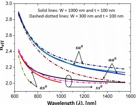
Initially, we study the wavelength (𝜆) dependencies of four possible fundamental SP modes, as shown in Fig. 3. Two different metal widths (W) 1000 nm and 500 nm for a fixed thickness, t = 100 nm are considered, shown by the solid and dotted lines, respectively. Ag dielectric constant is strongly 𝜆 dependent, determined here by the Kramers-Kronig relation [20] but the substrate and superstrate material is taken as a constant with its refractive index (𝑛𝑠𝑢𝑏𝑠𝑡𝑟𝑎𝑡𝑒 = 𝑛𝑠𝑢𝑝𝑒𝑟𝑠𝑡𝑟𝑎𝑡𝑒=
2) throughout the wavelength spectrum, ranging from 633 nm to 1550 nm. All the effective indices (𝑛𝑒𝑓𝑓) curves for
𝑠𝑠0, 𝑎𝑠0, 𝑠𝑎0 and 𝑎𝑎0 modes shown in Fig. 3 tend to converge
asymptotically to the surrounding refractive index (𝑛𝑠 = 2)
with the increasing 𝜆. The 𝑠𝑠0, 𝑠𝑎0 and 𝑎𝑎0 modes are guided
over a broad wavelength spectrum range whereas, the 𝑎𝑠0
mode shows a rapid approach to cut-off. The effective indices of 𝑠𝑎0 and 𝑎𝑎0 show almost similar 𝑛
𝑒𝑓𝑓 values for W = 1000
nm, however for a lower width (300 nm), these effective indices diverge from each other at higher 𝜆 and 𝑎𝑎0 mode
shows a much steeper asymptotic convergence to the background index values. This implies that for lower W/t ratio, only the 𝑠𝑎0 mode will exist for further higher
wavelengths. The 𝑠𝑠0 mode profile shows a field transition,
but not shown here. At lower operating wavelengths, the 𝑠𝑠0
mode supports distinct symmetric field confinement at four nanowire corners. That modal distribution is comparable with 𝑠𝑎0 mode, shown in Fig. 2(d) but with either all + or all – field
values at the four corners. As 𝜆 increases, the 𝑠𝑠0 field starts to evolve form four narrow corner spikes to the center of metal-dielectric interfaces so that the field makes a Gaussian like distribution along upper and lower interfaces, as shown in Fig. 2(b). This shows that at smaller 𝜆, fields are well confined, so weakly coupled and as a result more localized. No such 𝑠𝑎0 and 𝑎𝑎0 mode evolutions were observed over the
wavelength range considered here. Fig. 3. Dispersions of different plasmonic modes with the operating
wavelength (𝜆) ranging from 633 nm to 1550 nm. Fig. 4. Normalized effective indices variations of plasmonic modes with the surrounding identical material. The solid and dotted lines indicate the
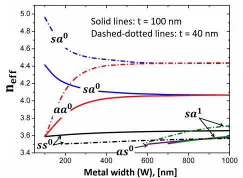
[image:5.612.322.558.52.238.2] [image:5.612.55.294.53.233.2]Fig. 5. 𝑛𝑒𝑓𝑓 variations of plasmonic modes with metal width (W). The
solid and dashed lines indicate the variations for two different thickness, t = 100 and 40 nm, respectively.
Figure 4 depicts how strong all the four fundamental modes approach the background supported TEM modes with the reduction in refractive index value of surrounding material, shown by the normalized effective index (𝑛𝑒𝑓𝑓/𝑛𝑠) variations.
In these cases, the wavelength is kept fixed at 1550 nm. Two different metal widths, W = 1000 and 500 nm with same thickness, t = 100 nm have been considered, shown by the solid and dotted lines, respectively. As the surrounding dielectric material refractive index decreases, for all plasmonic modes not only their effective indices decrease but also normalized effective index reduces and the mode fields spread more into the outer cladding. At a lower background refractive index, the modal effective indices approach the cladding refractive index value and their modal cut-off. The modes are then less bounded to the metal core and mostly guided by the background dielectric cladding, which also reduce the mode attenuation. Our study shows that the fundamental 𝑎𝑠0 and a
higher order 𝑠𝑎1 mode for W = 1000 nm only exist for a high
index cladding (𝑛𝑠 > 3.0) and approaches to the cut-off faster
than the other modes. The 𝑠𝑠0 for both W = 1000 and 500 nm,
reach to the cut-off earlier than the 𝑠𝑎0 and 𝑎𝑎0 modes. For
the background refractive indices lower than 1.7 and 2.0 for W = 1000 and 500 nm, respectively only 𝑠𝑎0 and 𝑎𝑎0 exist. With
reduction of metal W, the normalized effective indices of all the modes reach to the cut-off line i.e. 𝑛𝑒𝑓𝑓/𝑛𝑠 = 1 faster,
except for mode 𝑠𝑎0 which did not converge to the cut-off line
for the surrounding material of refractive index even when reached that of the free-space. Other 𝑎𝑎0 mode approaches to
cut-off for free-space cladding and here it evolves into background dielectric guided quasi-TEM mode with very low modal attenuation of 1 dB/mm. However, all these behaviors described are at the operating wavelength of 1550 nm, and their modal evolution changes with the wavelength as shown in Fig. 3.
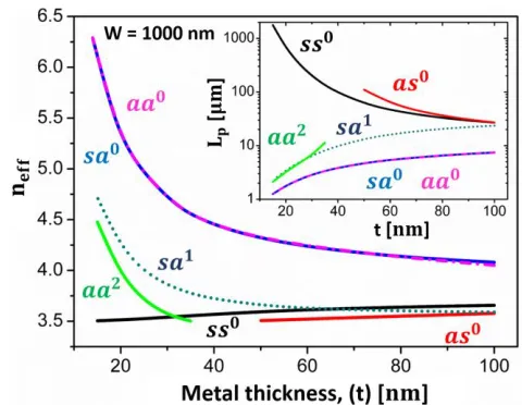
B. Modal Dependencies on Waveguide Dimension
Our study shows strong SPP modal dependence with the structural parameters (W and t) of the metal film. In both
cases, we assumed that the finite metal film is bounded by an identical medium, 𝑛𝑠𝑢𝑏𝑠𝑡𝑟𝑎𝑡𝑒 = 𝑛𝑠𝑢𝑝𝑒𝑟𝑠𝑡𝑟𝑎𝑡𝑒 = 3.5. Variations
of mode effective index (𝑛𝑒𝑓𝑓) with the W for two different t,
100 and 40 nm are shown in Fig. 5. The solid and dashed-dotted lines denote the modal 𝑛𝑒𝑓𝑓 variations for t = 100 and
40 nm, respectively. The 𝑛𝑒𝑓𝑓 of all modes (𝑎𝑎0, 𝑠𝑠0, 𝑎𝑠0 and
𝑠𝑎1) except 𝑠𝑎0 decrease with the reduction of W. For a large W, modes are well confined at the upper, lower and corners of the metal-dielectric interfaces. Decrease of modal effective indices towards the cladding refractive index indicates that the mode fields are less confined into lossy metal core and mostly spread into background dielectric medium. These also result less mode attenuation and consequently long modal propagation length (𝐿𝑝), as shown in Fig. 6. For wider W, the
symmetrical and asymmetrical fields of 𝑠𝑎0 and 𝑎𝑎0 modes,
respectively along x-direction are weakly coupled for a given thickness and both the modes travel with almost same propagation constants. As W reduces, symmetric corner fields of 𝑠𝑎0 mode along x-direction are strongly coupled with each
other and the corner fields also spread all along the upper and lower interfaces. Thus, 𝑠𝑎0 mode gets more confined and its
𝑛𝑒𝑓𝑓 increases when W reduces. On the other hand, for the
𝑎𝑎0 mode, due to asymmetrical corner field distributions,
fields cannot spread over the metal-dielectric interfaces rather dispersed into cladding medium. Hence its 𝑛𝑒𝑓𝑓 shows a
steeper reduction towards background refractive index. These also indicates higher and lower mode attenuations (𝛼) for the 𝑠𝑎0 and 𝑎𝑎0, respectively (Fig. 6). Additionally, with the
[image:6.612.320.558.50.239.2]reduction of t, the upper and lower interfaces come closer and the corner fields show a strong coupling as a result both the 𝑠𝑎0 and 𝑎𝑎0 modes show an increase of 𝑛
𝑒𝑓𝑓, away from the
background refractive index, shown in both Figs. 5 and 7. These also correspond to the higher mode attenuations and lower 𝐿𝑝 that can be seen in the Fig. 6 and inset of Fig. 7. The
symmetric mode field distributions along x and y-axes show a comparative low field confinement at the metal core rather mostly guided by the dielectric cladding. Thus, the 𝑛𝑒𝑓𝑓 of the
Fig. 6. The main and inset figures show the mode propagation length (𝐿𝑝) of different SPP modes with metal width (W) for different
[image:6.612.49.292.51.229.2]𝑠𝑠0 decreases and approaches towards the cut-off with
reduction of both W and t (Figs. 4 and 6). At the cut-off, modes evolve to the cladding supported quasi-TEM mode. Thus, its modal attenuation decreases and 𝐿𝑝 increases as it
approaches towards cut-off, shown in Figs. 5 and inset of 6. Another fundamental mode 𝑎𝑠0 (Fig. 2 (c)) with symmetric
field along y-axis only exists for higher W (Fig. 5) that approaches to cut-off early. This also results an increasing 𝐿𝑝
(Fig. 6) with W as it approaches its cut-off. This mode only exists for a limited range of t (do not exist for t < 50 nm, Fig. 7). This can also be observed in Fig. 7 where its 𝑛𝑒𝑓𝑓 and
mode attenuation decrease as the metal core thickness decreases. In this study, two fundamental modes 𝑠𝑠0 and 𝑎𝑠0 show a much lower modal attenuation (𝛼) of 2.4 dB/mm (W = 1000 nm and t = 15 nm) and 39.4 dB/mm (W = 1000 nm and t = 50 nm), respectively. Thus, it is expected that these modes can provide long range stability which could be useful for plasmonic based integrated optical applications. Besides the fundamental modes, we have also studied two higher order modes. Their mode evolutions are more complex. The 𝑠𝑎1
mode (Fig. 2 (f)) sustains over higher range of W, shown in Fig. 6. Due to its asymmetric field distribution along y-axis, the mode field gets more confined as t decreases. Thus, both of its 𝑛𝑒𝑓𝑓 and 𝛼 increase with the reduction of t (Fig. 7). Here
𝑎𝑎2 is another higher order mode with similar modal
properties that only appears when metal layer is thinner. Some of their modal properties can be seen in Figs. 4, 5 and 6.
V. NON-IDENTICAL CLADDING
Evolution of coupled plasmonic modes with truly 2D confinement, but with identical cladding materials are shown above. However, in most practical cases, upper and lower cladding materials can be totally different (𝑛𝑠𝑢𝑝𝑒𝑟𝑠𝑡𝑟𝑎𝑡𝑒≠
𝑛𝑠𝑢𝑏𝑠𝑡𝑟𝑎𝑡𝑒), hence not only their plasmonic modal profile will
changes but also their phase matching. Thus, our next study involves the evolutions of such modes and plasmonic supermode (PSM) for non-identical cladded metal nanowire.
Schematic of the structure was shown in Fig. 2 (a) but here with 𝑛𝑠𝑢𝑏𝑠𝑡𝑟𝑎𝑡𝑒 = 3.5 and 𝑛𝑠𝑢𝑝𝑒𝑟𝑠𝑡𝑟𝑎𝑡𝑒 = 3.3, a small index
difference is considered.
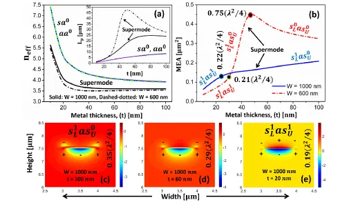
A. Asymmetric Mode Evolution with Waveguide Thickness (t)
In this section, we report the evolution of bound fundamentals and PSMs with metal film thickness (t) for two different widths (W). The modal 𝑛𝑒𝑓𝑓 and 𝐿𝑝 variations with
the t and W are shown in the main and inset of Fig. 8(a). Three different plasmonic modes, such as, a PSM and two fundamental modes (𝑠𝑎0 and 𝑎𝑎0) were identical during the
dimensional changes of metal film. For identical bounding material a given mode at upper and lower interfaces are always phase matched and they couple to form two complete symmetric and antisymmetric SP mode. Similarly, identical modes on the left and right interfaces couple to form SP modes. However, when the superstrate and substrate cladding materials are not the same, identical mode order cannot couple as their phase velocities are different, but modes of different orders at upper and lower (or left and right) interfaces can couples to form supermode but only when their propagation constants are similar. Here, the PSM forms due coupling of 𝑠𝑠0 and 𝑠𝑎1 like modes that we had observed for identical
clad metal waveguide. With different t, it shows a clear evolution which occurs due to coupling of individual upper and lower interface modes for a particular value of t. This PSM is named in a slightly different manner for better understanding, such as 𝐼𝐿𝑚𝐽𝐾𝑈𝑚. The first and third letters i.e. I
and K indicate either symmetric (s) or asymmetric (a) horizontal (along x) fields at the lower and upper interfaces with superscript ‘m’ as the number of intermediate localized
field maxima or minima that occurs at these interfaces. The second letter J also indicate either symmetric (s) or asymmetric (a) field distribution but along vertical (along y) direction. A notable field evolution for the long range asymmetrical PSM (𝑠𝐿𝑚𝑎𝑠𝑈𝑚) has been observed and its
parameter variations are shown with metal thickness (t) for a fixed W = 1000 nm. Figures 7(c), (d) and (e) depict the 𝐻𝑥
field profiles of that PSM for t = 100, 60 and 20 nm, respectively. In Fig. 8(c) the substrate (lower) interface field distribution exhibits two localized maxima at the corners and one minima at the center (𝑠1) whereas the superstrate (upper)
interface shows only two localized minima at the corners (𝑠0),
which combined to form a 𝑠𝐿1𝑎𝑠𝑈0 PSM. Two different
individual modes at upper and lower interfaces have the same propagation constant (𝛽) and together they form the 𝑠𝐿1𝑎𝑠𝑈0
PSM for t = 100 nm. As t decreases modes at both the interfaces start to interact as their coupling increases. The center maxima at the top interface grows gradually (Fig. 8(b)) due to a strong influence of the high index guided lower interface's 𝑠1 mode. Finally, at lower t = 20 nm, the upper
field completely evolved due to strong coupling and the metal waveguide shows a perfect 𝑠𝑎1 mode, as shown in Fig. 2(f)
which could also be named as 𝑠𝐿1𝑎𝑠𝑈1 PSM, shown in Fig. 8(e).
Its 𝑛𝑒𝑓𝑓 and 𝐿𝑝 variations with t for W = 1000 nm are shown
[image:7.612.49.289.50.236.2]by the solid black lines in the main and inset of Fig. 8(a), respectively. The mode effective area (MEA) variations (blue solid line in Fig. 8(b)) with t indicates a clear modal evolution. At higher thickness, till t ≈ 25 nm, the upper interface 𝑠0
Fig. 7. Plasmonic modal characteristics with metal nanowire thickness (t) for a fixed width, W = 1000 nm. The main plot shows the 𝑛𝑒𝑓𝑓 variations
mode evolves slowly whereas the 𝑠1 mode always maintain its
form at lower interface. Here, in the substrate with higher refractive index, the mode field localizes more strongly than the superstrate with a lower refractive index. The corresponding 𝑛𝑒𝑓𝑓 and MEA curves maintain a continuous
variation until t reaches around 25 nm. For the metal thickness, t = 25 nm the MEA shows the value of 0.22(𝜆2/4)
𝜇𝑚2. At lower t, due to the strong coupling between two
interfaces and low index superstrate guiding the upper 𝑠0
mode evolves faster and when t < 25 nm, its 𝑛𝑒𝑓𝑓 shows a
steeper increment away from the background dielectric refractive indices. The PSM becomes more localized and well confined into lossy metal core (Fig. 8(e)). Thus, its 𝐿𝑝 and
MEA decreases for a lower t. These PSM characteristics with t for a small non-identical clad waveguide also correlates with the combined behaviors of 𝑠𝑠0 and 𝑠𝑎1 modes for a
symmetrical waveguide shown in Fig. 7. This proves that this PSM is a blended form of 𝑠𝑠0 and 𝑠𝑎1 modes at two
interfaces.
For a lower W (600 nm), the PSM supported by a metal nanowire evolves with the variation of t, and show three different formations, such as 𝑠𝐿1𝑎𝑠𝑈1, 𝑠𝐿1𝑎𝑠𝑈0 and 𝑠𝐿0𝑠𝑠𝑈0 at
different metal core thicknesses. The black and red dashed-dotted lines in main and inset of Fig. 8(a) and (b) show the 𝑛𝑒𝑓𝑓, 𝐿𝑝 and MEA variations with t for a lower W = 600 nm,
respectively. It can be observed that as t decreases the 𝑛𝑒𝑓𝑓
decreases reaches a minimum value (nearly reach the
background refractive index). Below W = 600 nm the PSM approaches to the cut-off and fields are mostly guided by the surrounding dielectric media. 𝐿𝑝 variations also indicate the
modal evolution and a high 𝐿𝑝 value is obtained for W = 600
nm. The 1D 𝐻𝑥 field plot along x-axis of the PSM for t = 100,
40 and 20 nm at superstrate and substrate interfaces are shown in Fig. 9(a) and (b) by the green, red and blue solid lines, respectively. Based on the MEA and 𝐿𝑝 variations with t, one
can divide those curves into three distinct sections which signify three different forms of the PSM. At lower t (20 nm), the blue field profiles at upper and lower interfaces show the 𝑠1 distributions which couple to form a 𝑠
𝐿1𝑎𝑠𝑈1 PSM. This
mode exists for t = 10 to ∼ 30 nm. As t increases, its 𝑛𝑒𝑓𝑓
reaches to a minimum value at t = 48 nm and then further increases slightly. On the other hand, the 𝐿𝑝 and MEA both
possess maximum values at that thickness value when 𝑛𝑒𝑓𝑓
shows its minima. This low loss and high mode effective area indicate that the modal confinement was mostly in the surrounding dielectric materials. The field profiles shown by the red lines at both the interfaces indicate that a 𝑠𝐿1𝑎𝑠𝑈0 mode
exists over a thickness region t from ∼ 30 to 50 nm. The MEA
at these two metal thicknesses, t = 30 and 48 nm are 0.21 and 0.75 times of the diffraction limited mode area (𝜆2/4),
respectively. Beyond that, both the 𝐿𝑝 and MEA decreases
[image:8.612.53.555.217.510.2]faster with increase of t. At t = 100 nm, the field variations shown by the green lines at both interfaces show a completely Fig. 8. SPP modal characteristics its evolutions with metal thickness (t) for a metal nanowire with a small index-difference (𝑛𝑠𝑢𝑏𝑠𝑡𝑟𝑎𝑡𝑒 = 3.5 and 𝑛𝑠𝑢𝑝𝑒𝑟𝑠𝑡𝑟𝑎𝑡𝑒
= 3.3) in the cladding. The main and inset of (a) show the 𝑛𝑒𝑓𝑓 and 𝐿𝑝 variations of long range supermode, 𝑠𝑎0 and 𝑎𝑎0 modes for fixed W = 1000 nm and
600 nm shown by the solid and dashed-dotted lines, respectively. The solid blue and dashed-dotted lines in (b) depict the modal effective area (MEA) of supermodes for W = 1000 and 600 nm, respectively. (c), (d) and (e) denote the 𝐻𝑥 field evolution of the long range supermode for three different metal
Fig. 9. Normalized 𝐻𝑥 1D field plot of the long range supermode for
three different thickness, t = 100, 40 and 20 nm, shown by the solid green, red and blue lines, respectively. Corresponding mode effective area (MEA) are shown in (b). The metal nanowire width (W) is fixed at 600 nm. The top (𝑛𝑠𝑢𝑝𝑒𝑟𝑠𝑡𝑟𝑎𝑡𝑒 = 3.3) and bottom (𝑛𝑠𝑢𝑏𝑠𝑡𝑟𝑎𝑡𝑒 = 3.5)
interfaces field distributions are shown in sub-figures (a) and (b), respectively.
Fig. 10. Variations of plasmonic supermode (PSM) parameters in non-identical clad metal nanowire with core metal width (W) for different thickness, t = 20, 40, 60 and 80 nm shown by the black, blue, red and green lines, respectively. Variation of 𝑛𝑒𝑓𝑓 and corresponding 𝐿𝑝
variations with W are shown in sub-figures (a) and (b), respectively.
transformed nature of the PSM. The upper interface shows two symmetrical maxima at both the corners (𝑠0) whereas the
bottom interfaces shows only one Gaussian distribution with field maxima at the middle. These individual interface distributions combined to form a 𝑠𝐿0𝑠𝑠𝑈0 PSM. In short, with
increase of t, the top corner maxima exist throughout but the center minima vanish gradually, and for the lower interface the center maxima sustain but corner minima disappear. For lower W (600 nm) the left and right interfaces interact along with the upper and lower interfaces. Thus, the formed PSM shows evolution of field distributions along all the four metal-dielectric interfaces in the both x and y-directions.
For the conditions studied above, the two other fundamental modes 𝑠𝑎0 and 𝑎𝑎0 did not show any modal evolutions. As t
increases, its 𝑛𝑒𝑓𝑓 decreases in a rectangular hyperbolic
nature. Same 𝑛𝑒𝑓𝑓 and 𝐿𝑝 variation indicates that both the
modes propagate with almost same propagation constant and have almost similar modal attenuation.
B. Mode Evolutions with Core Width (W)
For a small cladding index difference, the width (W) dependent modal behaviors (𝑛𝑒𝑓𝑓 and 𝐿𝑝) of long rage PSM
have also been studied for different t = 20, 40, 60 and 80 nm, depicted by the black, blue, red and green lines, respectively in Figs. 9(a) and (b). The PSM for t = 20 nm shows a distinct trend than other PSMs guided by a higher thickness. These also prove the evolution of PSMs with metal waveguide
geometrical dispersion as already discussed in the previous section. The 𝑛𝑒𝑓𝑓 of PSM for t = 20 nm presented in Fig.
10(a), by a black line, shows a hyperbolic variation whereas other PSMs supported by metal core of t = 40, 60 and 80 nm show an almost exponential decay to the surrounding refractive index. For a thin metal core (t = 20 nm) both the upper and lower interfaces provide a strong coupling that makes the mode field more localized and confined into metal core. Influence of metal loss makes the modal attenuation high, yielding a smaller 𝐿𝑝 (Fig. 10(b)) than others. It is also
noticeable in Fig. 10(a) that the modes with thicknesses 40, 60 and 80 nm are loosely confined so that they approach faster towards the background quasi-TEM mode i.e. cut-off. However, this is not similar for the PSM supported by t = 20 nm as this is appeared to be a completely different mode.
C. Mode Evolutions Depending on Cladding Index
differences
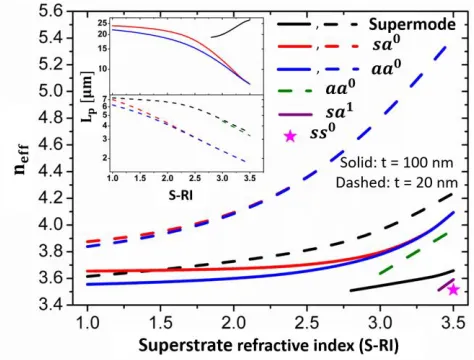
Besides the modal dependencies on the waveguide geometrical dimensions, the modal variations with different non-identical cladding conditions also have been investigated. The main and inset of Fig. 11 depicts the 𝑛𝑒𝑓𝑓 and 𝐿𝑝
variations of different modes with the variation of superstrate refractive index (S-RI). The substrate material refractive index was fixed at 3.5 for these simulations. The solid and dashed lines indicate different modes for t = 100 and 20 nm, respectively. The metal width was kept fixed at W = 1000 nm for both the thicknesses. The corresponding 𝐻𝑥 field profiles
of different guided modes at different conditions are shown in Figs. 11(a), (b), (c) and (d). The black, red, blue and green dashed lines indicate the 𝑛𝑒𝑓𝑓 and 𝐿𝑝 variations of supported
PSM, 𝑠𝑎0, 𝑎𝑎0 and 𝑎𝑎2 modes, respectively for t = 20 nm,
shown in main and inset of Fig. 11. The star marker indicates a long range 𝑠𝑠0 mode supported by this structure with
Fig. 11. 𝑛𝑒𝑓𝑓 and 𝐿𝑝 variations of different plasmonic modes with
superstrate refractive index (S-RI) shown by the main and the inset plots, respectively. The solid black, red, blue and purple lines indicate the PSM (𝑠𝐿1𝑎𝑠𝑈0), 𝑠𝑎0, 𝑎𝑎0 and 𝑠𝑎1 variations with S-RI, respectively for
waveguide dimension, W = 1000 nm and t = 100 nm. The dashed black, red, blue and green lines and pink star denote the guided PSM, 𝑠𝑎0, 𝑎𝑎0,
𝑎𝑎2 and 𝑠𝑠0 modal characteristics with S-RI for dimension, W = 1000
[image:9.612.51.291.52.166.2] [image:9.612.322.559.53.233.2] [image:9.612.54.291.258.359.2]attenuation 6.5 dB/mm only when the superstrate and substrate have the same refractive index 3.5. Here mostly the electromagnetic energy was guided by the background dielectric media. The black, red, blue and purple solid lines depict the 𝑛𝑒𝑓𝑓 and 𝐿𝑝 variations for PSM, 𝑠𝑎0, 𝑎𝑎0 and 𝑠𝑎1
modes, respectively for t = 100 nm, shown in main and top inset of Fig. 11. The PSM (𝑠𝐿1𝑎𝑠𝑈1) guided by the waveguide
with t = 20 nm sustained over the whole S-RI range and evolved into the 𝑠𝑎1 as both the upper and lower cladding
have the identical refractive index, shown by the black dashed lines. On the other hand, the PSM (𝑠𝐿1𝑎𝑠𝑈0 in Fig. 12(c)) for t =
100 nm reached to cut-off much faster at S-RI = 2.8, shown by the solid black lines. Thus, the PSM (𝑠𝐿1𝑎𝑠𝑈0) supported by the
t = 100 nm exists for small index difference of the background, shows a much lower modal attenuation and longer propagation length compared to the PSM that supported by t = 20 nm. With identical background, this mode completely evolves into 𝑠𝑠0 mode. The other two modes 𝑠𝑎0
and 𝑎𝑎0 for t = 20 nm propagates with almost the same
propagation constant with S-RI variations. Besides, for t = 100 nm these two modes have different propagation constants. The dominant 𝐻𝑥 field profiles of these two modes (when
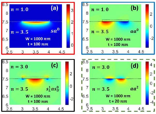
𝑛𝑠𝑢𝑝𝑒𝑟𝑠𝑡𝑟𝑎𝑡𝑒 = 1.0 and 𝑛𝑠𝑢𝑏𝑠𝑡𝑟𝑎𝑡𝑒 = 3.5) are shown Fig. 12(a)
and (b), respectively. In case of a large cladding index difference the fields were mostly guided by the substrate with higher refractive index. A higher order mode 𝑎𝑎2 (Fig. 12(d))
guided by t = 20 nm metal core shows its cut-off at S-RI = 2.8. The 𝑠𝑎1 (Fig. 2(f) like) and 𝑎𝑠0 (Fig. 2(b) like) modes are also guided by t = 100 nm metal core for very small cladding index difference.
VI. CONCLUSIONS
For this study, we have modified our previous penalty approach to consider waveguides which contains both positive and negative dielectric constants, to eliminate the spurious modes more efficiently in the characterizations of plasmonic modes. A detail modal investigation has been carried out to study nanoplasmonic modal behavior of guided modes supported by a simple metal (Ag) film embedded into dielectric background materials. Plasmonic modes have higher effective indices than the surrounding cladding refractive index. As they approach to cut-off, the mode fields spread into cladding region and plasmonic modes evolve into background quasi-TEM mode which leads to a reduction in mode propagation loss. Depending on different light guiding conditions long and short range plasmonic fundamental and higher order modes have been studied. The 𝑠𝑠0 and 𝑎𝑠0 are
the long-range modes for metal core bounded by identical cladding. At different cut-off conditions (W = 200 nm, t = 40 nm and W = 1000 nm, t = 15 nm), the 𝑠𝑠0 shows a much
lower attenuation of 8.9 dB/mm and 2.4 dB/mm compared to other guided modes. As the cladding becomes non-identical, a long range PSM appears due to coupling of different individual modes of all four metal-dielectric interfaces when they travel with similar propagation constant. An interesting notable modal evolution of this PSM was observed with its dimensions. A small thickness of metal film causes a strong upper and lower interface modal coupling which results a prominent modal evolution from 𝑠𝐿1𝑎𝑠𝑈0 to 𝑠𝐿1𝑎𝑠𝑈1 for W =
[image:10.612.145.467.52.288.2]1000 nm. On the other hand, for a smaller and near cut-off metal width (W = 600 nm) three different types of PSMs appeared due to modal coupling from all the four interfaces Fig. 12. The 𝐻𝑥 field distribution of different plasmonic modes of non-identical clad plasmonic waveguide simulated by FV-FEM, (a) and (b) depict the 𝑠𝑎0
and 𝑎𝑎0 field distributions for large index difference in the background (𝑛
𝑠𝑢𝑝𝑒𝑟𝑠𝑡𝑟𝑎𝑡𝑒= 1.0 and 𝑛𝑠𝑢𝑏𝑠𝑡𝑟𝑎𝑡𝑒 = 3.5) for metal thickness, t = 100 nm, (c) and (d)
show the field distributions of s𝐿1asU0 PSM and 𝑎𝑎2 when 𝑛𝑠𝑢𝑝𝑒𝑟𝑠𝑡𝑟𝑎𝑡𝑒 = 3.0 and 𝑛𝑠𝑢𝑏𝑠𝑡𝑟𝑎𝑡𝑒 = 3.5 for metal thickness, t = 100 and 20 nm, respectively. Metal
which makes the evolution process more complex. In that case, a comparative low modal attenuation with a large 𝐿𝑝 was
observed at a particular metal thickness, t = 48 nm. Additionally, surrounding dielectric cladding materials also influence the modal evolutions. Optically dense media confine and localize more light to the metal-dielectric interfaces than the optically lighter media. This also results in increase of
MEA with the reduction of cladding index.
Thus, the numerically investigated bounded SPP modal analyses of a simple Ag nanowire successfully demonstrate the usefulness of our proposed divergence modified FV-FEM. Besides, these attractive nanoplasmonic modal natures with different light guiding conditions gives intuitive ideas in design and fabrication of complex plasmonic devices, such as logic gates, switch, BUS router, modulator and nanowire laser. An appropriate selection of background dielectric materials and metal nanowire design parameters could lead to control the long-range subwavelength confined plasmonic modes and their incorporation in compact integrated plasmonic and hybrid plasmonic active and passive nanophotonic circuits [21], [22], polarization controlling devices [7], [22], nonlinear [23] and sensing [8], [9], [22], [24] applications.
REFERENCES
[1] D. M. H. Leung, B. M. A. Rahman, N. Kejalakshmy, and K. T. V. Grattan, “Rigorous full-vectorial solutions of photonic nanowires,” IEEE Journal of Quantum Electronics, vol. 40, 325 – 329, 2011.
[2] D. M. H. Leung, N. Kejalakshmy, B. M. A. Rahman, and K. T. V. Grattan, “Rigorous modal analysis of silicon strip nanoscale waveguides,” Opt. Express, vol. 18, 8528 – 8539, 2010.
[3] G. Veronis and S. Fan, “Modes of subwavelength plasmonic slot waveguides,” J. Lightw. Technol., vol. 25, 2511 – 2521, 2007. [4] D. Dai and S. He, “A silicon-based hybrid plasmonic waveguide with a
metal cap for a nano-scale light confinement,” Opt. Express, vol. 17, 16646 – 16653, 2009.
[5] Y. Bian and Q. Gong, “Bow-Tie hybrid plasmonic waveguides,” J. Lightw. Technol., vol. 32, 4504 – 4509, 2014.
[6] M. Z. Alam, J. Meier, J. S. Aitchison, and M. Mojahedi, “Propagation characteristics of hybrid modes supported by metal-low-high index waveguides and bends,” Opt. Express, vol. 18, 12971 – 12979, 2010. [7] M. Z. Alam, J. S. Aitchsion, and M. Mojahedi, “Compact hybrid
TM-pass polarizer for silicon-on-insulator platform,” App. Opt., vol. 50, 2294 – 2298, 2011.
[8] S. Ghosh and B. M. A. Rahman, “Full vectorial finite element modelling: a composite plasmonic horizontal slot waveguide as a bio-sensor,” 13th International Conference on Fiber Optics and Photonics 2016, https://doi.org/10.1364/PHOTONICS.2016.Tu5C.3.
[9] S. Ghosh and B. M. A. Rahman, “A compact Mach-Zehnder interferometer using composite plasmonic waveguide for ethanol vapor sensing,” J. Lightw. Technol., vol. 35, 3003 – 3011, 2017.
[10] A. D. Berk, “Variational principles for electromagnetic resonators and waveguides,” IRE Trans. Antennas Propag., vol. 4, 104 –- 111, 1956. [11] B. M. A. Rahman and J. B. Davies, “Finite-element solution of
integrated optical waveguides,” J. Lightw. Technol., vol. 2, 682 – 688, 1984.
[12] B. M. A. Rahman and J. B. Davies, “Penalty function improvement of waveguide solution by finite element,” IEEE Trans. Microw. Theory Techn. vol. 32, 922 – 928, 1984.
[13] S. Ghosh and B. M. A. Rahman, “An innovative straight resonator incorporating a vertical slot as an efficient bio-chemical sensor,” IEEE J. Sel. Top. Quantum Electron., vol. 23, 132 – 139, 2017.
[14] J. J. Burke, G. I. Stegeman, and T. Tamir, “Surface-polariton-like waves guided by thin, lossy metal films,” Phys. Rev. B, vol. 33, 5186 – 5201, 1986.
[15] R. Zia, M. D. Selker, P. B. Catrysse, and M. L. Brongersma, “Geometries and materials for subwavelength surface plasmon modes,” J. Opt. Soc. Am. A, vol. 21, 2442 – 2446, 2004.
[16] C. Themistos, B. M. A. Rahman, and K. T. V. Grattan, “Finite-element analysis of surface-plasmon modes for lossy optical waveguides by the use of perturbation techniques,” Appl. Opt., vol. 34, 7695 – 7701, 1995. [17] R. Zia, M. D. Selker, and M. L. Brongersma, “Leaky and bound modes
of surface plasmon waveguides,” Phys. Rev. B, vol. 71, 165431-1 – 165431-9, 2005.
[18] P. Berini, “Plasmon-polariton waves guided by thin lossy metal films of finite width: Bound modes of asymmetric structures,” Phys. Rev. B, vol. 63, 125417-1 – 15, 2001.
[19] P. Berini, “Plasmon-polariton waves guided by thin lossy metal films of finite width: Bound modes of symmetric structures,” Phys. Rev. B, vol. 61, 10484 – 10503, 2000.
[20] S. Babar and J. H. Weaver, “Optical constants of Cu, Ag, and Au revisited,” Appl. Opt., vol. 54, 477 – 481, 2015.
[21] H. Wei, Z. Wang, X. Tian, M. Kall and H. Xu, “Cascaded logic gates in nanophotonic plasmon networks,” Nat. Commun., vol. 2, 387-1 – 5, 2011.
[22] D. Dai, H. Wu, and W. Zhang, “Utilization of field enhancement in plasmonic waveguides for subwavelength light-guiding, polarization handling, heating, and optical sensing,” Materials, vol. 8, 6772 – 6791, 2015.
[23] F. J. Diaz, T. Hatakeyama, J. Rho, Y. Wang, K. O’Brien, X. Zhang, C. Martijn de Sterke, B. T. Kuhlmey, and S. Palomba, “Sensitive method for measuring third order nonlinearities in compact dielectric and hybrid plasmonic waveguides,” Opt. Express, vol. 24, 545 – 554, 2016. [24] P. Berini, “Bulk and surface sensitivities of surface plasmon
waveguides,” New J. Phys., vol. 10, 1 – 37, 2008.
Souvik Ghosh was born in Kolkata, India. He received his B.Tech and M.Tech degree in Optics and Optoelectronics (First class, 1st rank) from Calcutta University (C.U), India in 2012 and 2014, respectively. He is currently pursuing Ph.D. degree at the School of Mathematics, Computer Science and Engineering, City, University of London, U.K. He is also a recipient of Erasmus Mundus Areas+ Ph.D. fellowship and SPIE Optics and Photonics Education Scholarship, 2017. His research interests include the application of two dimensional and three-dimensional finite element method in photonic devices, waveguides as well as resonators. Currently he is working on the development and application of finite element method for simulation of complex plasmonic waveguides and resonators.
B. M. A. Rahman (S’ 80 - M’83 – SM’94 – F’2016) received his B.Sc Eng. And M.Sc. Eng. Degrees (with distinctions) in Electrical Engineering from the Bangladesh University of Engineering and Technology (BUET), Dhaka, Bangladesh, in 1976 and 1979, respectively, and received two gold medals for being the best undergraduate and graduate students of the university in 1976 and 1979, respectively. In 1979, he received a Commonwealth Scholarship and in 1982 obtained a Ph.D. degree in Electronics from University College London, London, U.K.
etc. He is the author or co-author of more than 500 journal and conference papers, and his journal papers have been cited more than 4200 times. He is a Fellow of the IEEE, Optical Society of America (OSA) and SPIE.