City, University of London Institutional Repository
Citation
:
Cabrera-Espana, F. (2017). Analysis of the optical properties of texturingpatterns for design of Si solar cells. (Unpublished Doctoral thesis, City, Universtiy of London)
This is the accepted version of the paper.
This version of the publication may differ from the final published
version.
Permanent repository link:
http://openaccess.city.ac.uk/19766/Link to published version
:
Copyright and reuse:
City Research Online aims to make research
outputs of City, University of London available to a wider audience.
Copyright and Moral Rights remain with the author(s) and/or copyright
holders. URLs from City Research Online may be freely distributed and
linked to.
City Research Online: http://openaccess.city.ac.uk/ [email protected]
Analysis of the optical properties of
texturing patterns for design of
Si solar cells
Francisco José Cabrera España
School of Mathematics, Computer Sciences and Engineering
City, University of London
This thesis is submitted for the degree of
Doctor of Philosophy
3 TABLE OF CONTENTS
TABLE OF CONTENTS 3
LIST OF FIGURES 7
LIST OF TABLES 11
ACKNOWLEDGEMENTS 13
DECLARATION 15
ABSTRACT 17
LIST OF ABBREVIATIONS 19
LIST OF SYMBOLS 21
Chapter 1: Introduction 25
1.1 Importance of solar cells 25
1.2 History of solar cells 26
1.3. Inorganic solar cells 27
1.3.1. Basic P-N junction and single junction solar cells 28 1.3.1.1 Forward biased p-n junction 30 1.3.1.2 Reverse biased p-n junction 31 1.3.1.3 I-V Curve of a p-n junction 31 1.3.1.4 Single junction solar cell 32 1.3.1.5 Schockley-Queisser limit 41
1.3.2 Multijunction solar cells 42
1.3.3 Crystalline Silicon solar cells 44
1.3.4 Thin film solar cells 45
1.3.4.1 Amorphous Silicon (a-Si) solar cells 45 1.3.4.2 Cadmium Telluride (CdTe) solar cells 46 1.3.4.3 Copper Indium Gallium Selenide (CIGS) solar cells 47
1.3.5 Concentrated solar cells 48
1.4 Organic solar cells 49
1.4.1 Inorganic-Organic Perovskite solar cells 51 1.5 Different techniques to lower Reflectance 53
1.5.2 Anti reflection coatings 53
1.5.3 Plasmonic solar cells 54
1.5.4 Surface Texturing of solar cells 56
1.5.4.1 Pyramid solar cells 57
4
1.5.4.3 Nanowall solar cells 59
1.5.4.4 Moth eye solar cells 61
1.5.4.5 Nanocone solar cells 63
1.5.4.6 Micro pillar solar cells 64
1.6 Summary 65
1.7 References 67
Chapter 2: Methodology 83
2.1 Importance of Numerical methods 83
2.2 Maxwell’s equations 88
2.3 Finite-Difference-Time-Domain (FDTD) Method 90 2.3.1 Time discretization of the FDTD method (Leap frog approach) 91 2.3.2 Space discretization of the FDTD method 92 2.3.3 Mesh accuracy and stability 94
2.3.4 Finite differences 97
2.3.5 Governing equations of the 3D FDTD method 99
2.3.6 Simulation set up 102
2.3.6.1 Location of the monitor and the source 103
2.3.6.2 Window height 104
2.3.6.3 Mesh parameters 107
2.3.6.4 Number of PML layers 109
2.3.6.5 Representing the different structures under study 111 2.3.6.6 Processing of the results 115 2.3.7 AM 1.5 reference solar spectrum and plane-wave source 116
2.3.8 Boundary conditions 118
2.3.8.1 Perfect Electric Conductor (PEC) and Perfect Magnetic Conductor
(PMC) 119
2.3.8.2 Periodic Boundary Conditions (PBC) 121 2.3.8.3 Absorbing Boundary Condition (ABC) 123 2.3.8.3.1 Perfectly Matched Layer (PML) 124
2.4 Summary 126
2.5 References 129
Chapter 3: Silicon solar cell with micro pillar array texture 133
3.1 Introduction 133
5
3.4 Effect of Diameter on the reflection from the solar cell 145 3.5 Effect of Surface Coverage and space between pillars on the reflection from
the solar cell 149
3.6 Impact of H/D ratio on the reflection from the solar cell 157
3.7 Summary 162
3.8 References 165
Chapter 4: Hut-like Si micro pillar array 167
4.1 Introduction 167
4.2 Comparison with other patterns 169 4.3 Effect of , SC and Cap on area in between huts 173 4.4 Effect of H on the reflection from the surface of the solar cell 183 4.5 Effect of D on the reflection from the surface of the solar cell 185 4.6 Effect of Cap on the reflection from the surface of the solar cell 187 4.7 Identifying an optimum set of parameters 195 4.8 Proof of concept by experimental results 196
4.9 Summary 200
4.10 References 203
Chapter 5: Conclusions and recommendations for further work 207
5.1 Introduction 207
5.2 Summary of the research 207
5.3 Recommendations for further work 209
Appendix A 211
Appendix B 215
7
LIST OF FIGURES
FIG. 1.1. SCHEMATIC DIAGRAM OF A P-N JUNCTION. A) WITHOUT DEPLETION REGION. B) WITH
DEPLETION REGION. ... 28
FIG. 1.2. 1D DIAGRAMS OF A P-N JUNCTION UNDER EQUILIBRIUM STATE. (A) ELECTRIC FIELD. (B) VOLTAGE. ... 29
FIG. 1.3. SCHEMATIC OF A P-N JUNCTION ON FORWARD BIASED OPERATION. ... 30
FIG. 1.4. SCHEMATIC OF A P-N JUNCTION ON REVERSE BIASED OPERATION. ... 31
FIG. 1.5. TYPICAL I-V CURVE OF P-N JUNCTION DIODE. ... 32
FIG. 1.6. SCHEMATIC OF A SINGLE JUNCTION SOLAR CELL. ... 32
FIG. 1.7. REFLECTIVITY VS. WAVELENGTH CURVE FROM THE PLANAR AIR-SILICON INTERFACE. INSET 1 REAL AND IMAGINARY PARTS OF THE REFRACTIVE INDEX OF SI. ... 34
FIG. 1.8. SCHEMATIC OF ELECTRON TRANSITION FOR A) DIRECT AND B) INDIRECT BAND GAP. ... 35
FIG. 1.9. EFFICIENCY VS. ENERGY BAND GAP OF THE ACTIVE MATERIAL ACCORDING TO THE DETAILED BALANCED ANALYSIS PRESENTED BY SHOCKLEY AND QUEISSER. ... 42
FIG. 1.10. TYPICAL CONCENTRATED SOLAR CELL ... 48
FIG. 1.11. SCHEMATIC OF A BULK-HETEROJUNCTION SOLAR CELL ... 50
FIG. 1.12. SCHEMATIC OF PYRAMID TEXTURING PATTERN. ... 57
FIG. 1.13. SCHEMATIC OF NANOWIRE TEXTURING PATTERN. ... 58
FIG. 1.14. SCHEMATIC OF THE NANOWALL PATTERN. (A) SIDE VIEW. (B) TOP VIEW. ... 59
FIG. 1.15. SCHEMATIC OF THE RESULTING TEXTURING PATTERN WHEN COMBINING NANOWALLS AND NANOWIRES. ... 60
FIG. 1.16. IMAGE OF A MOTH AND THE IMAGE OF THE ZOOMED EYE OF THE MOTH. ... 61
FIG. 1.17. SCHEMATIC OF THE MOTH EYE CONED STRUCTURE. ... 62
FIG. 1.18. (A) SCHEMATIC OF A NANOCONE ARRAY. (B) TOP VIEW OF THE PATTERN. ... 63
FIG. 2.1. SCHEMATIC ILLUSTRATING THE STAIRCASING ERROR CAUSED BY THE IMPLEMENTATION OF THE MESH IN THE FDTD METHOD. ... 85
FIG. 2.2. SCHEMATIC SHOWING THE REASON FOR NUMERICAL DISPERSION IN THE CASE OF X=Y=Z. 88 FIG. 2.3. SCHEMATIC DIAGRAM OF LEAP-FROG APPROACH ... 91
FIG. 2.4. YEE LATTICE. ... 93
FIG. 2.5. 2D SCHEMATIC SHOWING MESH PARAMETERS X AND Y. ... 94
FIG. 2.6. SCHEMATIC EXPLAINING THE YEE NOTATION FOR THE CASE OF “I”. ... 99
FIG. 2.7. SCHEMATIC ILLUSTRATING THE CONSIDERATIONS DURING THE SETTING UP PROCESS. ... 102
FIG. 2.8. SCHEMATIC OF SIMULATION SET UP. ... 103
FIG. 2.9. SCHEMATIC FOR THE SELECTION OF WINDOW HEIGHT. ... 104
FIG. 2.10 E FIELD INTENSITY VS. TIME AT REFLECTION MONITOR AND BOUNDARY OF WINDOW. ... 106
FIG. 2.11. E FIELD INTENSITY NEAR THE REFLECTION MONITOR AT A. 20FS AND B.124FS. ... 106
FIG. 2.12. PERCENTAGE OF THE SIMULATION ERROR OF R PER WAVELENGTH AS VARYING Z WHILE KEEPING CONSTANT X AND Y AT 0.01µM. ... 108
FIG. 2.13. RINT VS. NUMBER OF PML LAYERS. ... 110
FIG. 2.14. SCHEMATIC OF MICRO PILLARS. ... 111
FIG. 2.15. SCHEMATIC OF HEXAGONAL ARRAY CONFIGURATION. ... 112
FIG. 2.16. SCHEMATIC OF PROPOSED HUT-LIKE MICRO PILLAR ARRAY. INSET 1 TOP VIEW OF HUT-LIKE PATTERN. ... 113
FIG. 2.17. AM 1.5 REFERENCE SOLAR SPECTRUM. ... 117
FIG. 2.18. SCHEMATIC USING SYMMETRY TO REPLICATE A MICRO PILLAR FROM 1 QUARTER OF THE STRUCTURE. ... 120
FIG 2.19. SCHEMATIC SHOWING THE UNIT CELL OF A PERIODIC STRUCTURE. ... 121
FIG. 2.20. ILLUSTRATION OF THE MAPPING OF PBC IN X-Y PLANE. ... 122
FIG. 2.21. SPURIOUS REFLECTION FROM THE TRUNCATED BOUNDARY. ... 123
8
FIG. 3.1. R VS. WAVELENGTH FOR HEXAGONAL AND SQUARE CONFIGURATIONS WHEN H= 1µM, D=
1µM AND SC= 60%. ... 135
FIG. 3.2. RINT VS. SC FOR HEXAGONAL AND SQUARE CONFIGURATIONS. ... 136
FIG. 3.3. E FIELD INTENSITY AT A CROSS SECTION FOR THE CASE OF HEXAGONAL CONFIGURATION. ... 138
FIG. 3.4. E FIELD INTENSITY AT A CROSS SECTION FOR THE CASE OF SQUARE CONFIGURATION. ... 138
FIG. 3.5. RINT VS. SC FOR HEXAGONAL AND SQUARE CONFIGURATIONS FOR THE CASE OF H=1 µM AND D= 2µM. ... 139
FIG. 3.6. EFFECT OF VARYING H FOR FIXED D (=2 µM). ... 140
FIG. 3.7. EFFECT OF VARYING H FOR FIXED D (=1 µM). ... 141
FIG. 3.8. E FIELD INTENSITY IN A VERTICAL CROSS SECTION FOR THE CASE OF (A) H=1 µM, D=1 µM AND SC= 40% (B) H=2 µM, D= 1µM AND SC= 40% (C) H= 5 µM, D= 1µM AND SC= 40% AT Λ= 0.363636. ... 143
FIG. 3.9. E FIELD INTENSITY IN A VERTICAL CROSS SECTION FOR THE CASE OF (A) H= 1µM, D= 1µM AND SC= 50% (B) H= 2µM, D= 1µM AND SC= 50% (C) H= 5µM, D= 1µM AND SC= 50% AT Λ= 0.363636µM. ... 144
FIG. 3.10. EFFECT OF VARYING D FOR FIXED H OF 2µM WITH RESPECT TO SC (SOLID LINES IN BLUE, RED AND GREEN) AND SPACE BETWEEN PILLARS (DASHED LINES IN BLUE, RED, GREEN AND CYAN). . 146
FIG. 3.11. SCHEMATIC OF THE SET UP FOR STUDYING EFFECT OF VARYING SC. ... 149
FIG. 3.12. E FIELD INTENSITY AT MONITORS S, M AND A FOR PILLAR H= D= 2µM AND SC= 60%. ... 150
FIG. 3.13. E FIELD INTENSITY AT MONITORS S, M AND A FOR PILLAR H= D= 2µM AND SC= 80%. ... 151
FIG. 3.14. E FIELD INTENSITY AT MONITORS S, M AND A FOR PILLAR H= D= 2µM AND SC= 50%. ... 152
FIG. 3.15. SIMULATION SET UP TO OBTAIN E FIELD PLOTS AS SC VARIES. ... 153
FIG. 3.16. E FIELD INTENSITY OF A CROSS SECTION AT 0.2µM ABOVE THE SUBSTRATE FOR THE CASE OF H= 1µM, D= 1µM AND SC= 60%. ... 153
FIG. 3.17. E FIELD INTENSITY OF A CROSS SECTION AT 0.2µM ABOVE THE SUBSTRATE FOR THE CASE OF H= 1µM, D= 1µM AND SC=80%. ... 154
FIG. 3.18. E FIELD INTENSITY OF A CROSS SECTION AT 0.2µM ABOVE THE SUBSTRATE FOR THE CASE OF H= 1µM, D= 1µM AND SC=50%. ... 155
FIG. 3.19. RINT WHEN VARYING SPACE BETWEEN PILLARS AND SC, WITH A) D= 3µM AND B) D= 1µM. 156 FIG. 3.20. RINT VARIATION WITH H/D RATIO AND KEEPING D FIXED FOR 50% SC. ... 158
FIG. 3.21. R VARIATION WITH H/D RATIO AND KEEPING D FIXED FOR 40% SC. ... 159
FIG. 3.22. EFFECT OF LARGE H/D (RATIO=1) ON R VS. WAVELENGTH FOR 40% SC. ... 161
FIG. 3.23. EFFECT OF LARGE H/D (RATIO=10) ON R VS. WAVELENGTH FOR 40% SC. ... 162
FIG. 4.1. R VS. WAVELENGTH CURVE COMPARISON BETWEEN THE HUT-LIKE STRUCTURE (D= 1µM, H= 1µM AND =115) WITH OTHER TEXTURING PATTERNS OF SIMILAR DIMENSIONS. ... 171
FIG. 4.2. ANGULAR PERFORMANCE, AREA IN BETWEEN THE HUTS VS FOR H= 1 µM, RADIUSTOP = 0.5 µM AND CAP= 0.2 µM WHERE THE LINE COLOUR REPRESENTS RINT. ... 175
FIG. 4.3. RINT VS. FOR THE SC VALUES: 30%, 40% AND 50%. ... 176
FIG. 4.4. VARIATION OF AREA IN BETWEEN HUTS VS. FOR SC VALUES: 30%, 40% AND 50%. INSET 1. CHANGE IN EFFH AS AREA IN BETWEEN HUT DECREASES. ... 177
FIG 4.5. SCHEMATIC OF AN OVERLAPPED HUT-LIKE PATTERN. ... 177
FIG. 4.6. SCHEMATIC OF AN OVERLAPPED HUT-LIKE PATTERN FROM A TOP VIEW. ... 178
FIG. 4.7. CROSS SECTION SHOWING E FIELD INTENSITY AT 0.2 M ABOVE THE SUBSTRATE FOR STRUCTURE WITH H= 1 M, CAP = 0.2 M AND SC = 30 % AT 0.373 M FOR A) =90, B) =105 AND C): =115 (I.E. OPTIMUM). ... 178
FIG. 4.8. CROSS SECTION SHOWING E FIELD INTENSITY AT VERTICAL CROSS SECTION (X-Z PLANE) OF THE STRUCTURE WITH H= 1 M, CAP = 0.2 M AND SC = 30 % AT 0.373M FOR A) =90, B) =105, C) =115 (I.E. OPTIMUM) AND D) =125. ... 179
FIG. 4.9. EFFECT IN AND THE AREA IN BETWEEN HUTS AS CAP VARIES. ... 181
9
FIG. 4.11. VARIATION IN RINT AS THE AREA IN BETWEEN HUTS CHANGES, FOR DIFFERENT H. ... 183
FIG. 4.12. EFFECT OF D AT SC= 30% FOR THE CASE OF D= 0.5µM, 1µM, 1.5µM, 2µM. ... 186
FIG. 4.13. RINT VS. AT SC= 30% VARYING CAP SIZE FOR H=1 M. ... 187
FIG. 4.14. RINT VS. AT SC=30 % VARYING CAP SIZE FOR H=2 M. ... 189
FIG. 4.15. RINT VS. AT SC=30 % VARYING CAP SIZE FOR H=2 M. ... 190
FIG 4.16. SCHEMATIC OF INCREASE IN SLOPED PART AS H INCREASES FOR CONSTANT CAP/H RATIO. . 191
FIG. 4.17. RINT VS. SC CURVE WHILE VARYING CAP SIZE FOR H= 1µM AND =115. ... 192
FIG. 4.18. E FIELD INTENSITY AT A VERTICAL CROSS SECTION AT SC=40% IN THE CASE OF A) CAP= 0.2µM AND B) CAP= 0.0µM. ... 193
FIG. 4.19. E FIELD INTENSITY AT A VERTICAL CROSS SECTION AT SC=20% IN THE CASE OF A) CAP= 0.2µM AND B) CAP= 0.0µM. ... 194
FIG. 4.20. RINT VS OPTIMUM Θ FOR DIFFERENT VALUES OF H AND SC WITH CAP = 0.2M. ... 195
FIG. 4.21. CROSS-SECTION SEM IMAGE OF AFTER 20 MINS ETCHING SHOWING =124. ... 197
FIG. 4.22. PLANAR SEM IMAGE OF AFTER 20 MINS ETCHING. ... 198
FIG. 4.23. R VS. WAVELENGTH CURVE COMPARISON BETWEEN THE HUT-LIKE STRUCTURE (D= 1µM, H= 1µM AND =115) INCLUDING EXPERIMENTAL RESULTS WITH OTHER TEXTURING PATTERNS OF SIMILAR DIMENSIONS. ... 199
City, University of London Northampton Square London EC1V 0HB United Kingdom
T +44 (0)20 7040 5060
www.city.ac.uk Academic excellence for business and the professions
THE FOLLOWING PART OF THIS THESIS H
AS
BEEN REDACTED
FOR COPYRIGHT REASONS:
11 LIST OF TABLES
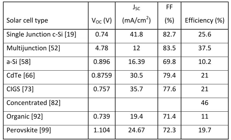
TABLE 1.1. SUMMARY OF BEST ELECTRICAL PERFORMANCE FOR EACH SOLAR CELL TYPE. 53 TABLE 2.1. RELATION BETWEEN MESH PARAMETERS AND MEMORY REQUIREMENTS AND SIMULATION
TIME. 87
TABLE 2.2. RELATION BETWEEN MESH PARAMETERS AND TIME STEP. 97 TABLE 4.1. COMPARISON OF MEMORY REQUIREMENTS AND SIMULATION TIME IN VERTICAL MICRO
13
ACKNOWLEDGEMENTS
My utmost gratitude goes to City, University of London and the School of Mathematics, Computer Science and Engineering and all the staff involved for allowing me to complete this PhD fully funded.
My most sincere gratitude goes to my first supervisor Dr. Arti Agrawal, who has guided me through this research. She has spent a lot of her time to direct me towards a constant development of this research. I am also grateful to my co-supervisor Prof. Dr. B. M. A. Rahman who has shared his point of view whenever he was asked.
Furthermore, I would like to express my gratitude to Prof. Hari Reehal from London South Bank University for characterizing the samples of the solar cell proposed in this work. Additionally, my gratitude also goes to Dr. Philip Shields from the University of Bath for fabricating the sample of the solar cell proposed in this work.
I would also like to express my gratitude to my colleagues in the Lab where we have spent many hours together. They shared their experiences with me when I was starting my research.
15
DECLARATION
I hereby declare that except where specific reference is made to the work of others, the contents of this dissertation are original and have not been submitted in whole or in part for consideration for any other degree or qualification in this, or any other University. This dissertation is the result of my own work and includes nothing which is the outcome of work done in collaboration, except where specifically indicated in the text. This dissertation contains less than 65,000 words including appendices, references, footnotes, tables and equations and has less than 150 figures.
17
ABSTRACT
The pronounced development in the field of solar cells has been driven by the increasing interest in “green” energy generation in recent decades. Nevertheless, to increase the deployment of solar cells the energy conversion efficiency has to be improved further. The highest energy conversion efficiency has been recorded using a Silicon solar cell. However, there are limitations such as the high reflection from the solar cell surface that limits further improvement of the energy conversion efficiency. The large refractive index contrast between air and the material of the solar cell leads to high reflection. As a consequence, reducing the reflection from the solar cell surface is a priority.
This research aims at reducing reflection from the solar cell surface. To achieve this goal, modeling based analysis of a micro pillar array texturing pattern and a new and exciting texturing pattern (the hut-like pattern) are presented. The simulation method used for this study is the Finite Difference Time Domain (FDTD) method. In the discussion, the effect of key structural parameters on the reflection is analyzed to obtain an in-depth understanding of the patterns. Additionally, the inter-dependence between the different structural parameters under study is considered during the discussion.
The analysis shows that the reflection from a micro pillar array solar cell decreases as the Height (H) increases. The H by Diameter (H/D) ratio analysis presented in this work determines that there is a convergence in the reflection when the H/D ratio is high. This can be useful especially for designers with low precision fabrication equipment who can target higher H/D ratio to ensure a low reflection. The high surface-to-volume ratio when the H/D ratio is high can lead to high surface recombination. High surface recombination is a major problem in textured solar cell since it diminishes the electrical performance.
19
LIST OF ABBREVIATIONS
Silicon (Si)
Amorphous silicon (a-Si) Cadmium Telluride (CdTe)
Copper Indium Gallium Selenide (CIGS) Gallium Arsenide (GaAs)
Gallium Selenide (GaSe) Germanium (Ge)
Gallium Phosphite (GaP) Fill Factor (FF)
Open Circuit Volage (Voc) Short Circuit Current (Isc) Crystalline Silicon (c-Si)
Copper Phthalocynanine (CuPc) Anti Reflection Coating (ARC)
Finite Difference Time Domain (FDTD) Contour Path FDTD (CP FDTD)
Perfectly Matched Layer (PML) Periodic Boundary Conditions (PBC) Reflectance (R)
Reflectance integrated overall wavelengths (RInt) Height (H)
Diameter (D)
Surface Coverage (SC)
Air Mass 1.5 reference solar spectrum (AM 1.5) Extraterrestrial (Ext)
Perfectly Electric Conductor (PEC) Absorbing Boundary Condition (ABC) Perfect Magnetic Conductor (PMC) Height by Diameter (H/D)
Cap by Height (Cap/H)
Deep Reactive Ion Etching Process (DRIE) Rapid Thermal Oxidation (RTO)
21
LIST OF SYMBOLS
n Refractive index of the material i
k
Initial electron momentumf
k
Final electron momentumq
Photon momentumi
E
Initial associated energy with photon fE
Final associated energy with photon
Associated energy
h Energy of a photon Absorption coefficient
ph
E Photon energy
g
E Energy band gap
A Direct band gap material constant B Indirect band gap material constant FF Fill factor
OC
V Open circuit voltage
SC
I Short circuit current
M P
V Voltage at maximum power
MP
I Current at maximum power
Conversion efficiency
IN
P Power of incoming light
B Magnetic flux density E Electric field
xE
Curl of E
M Magnetic current density
D Electric current density H Magnetic field
22 Electric permittivity
r
Relative permittivity
0
Free-space permittivity
Magnetic permeabilityr
Relative permeability
0
Free-space permeability
x
Mesh step size on the x direction
y
Mesh step size on the y direction
z
Mesh step size on the z direction
t
Time step
u x
Function dependent on x
u' x
First derivative of a function dependent on xi Current node in the FDTD scheme in x direction j Current node in the FDTD scheme in y direction k Current node in the FDTD scheme in z direction n Current node in the FDTD scheme in time i+1 Next node in the FDTD scheme in x direction
i-1 Previous node in the FDTD scheme y direction
x
E Electric field component on the x direction
y
E Electric field component on the y direction
z
E Electric field component on the z direction
x
H Magnetic field component on the x direction
y
H Magnetic field component on the y direction
z
H Magnetic field component on the z direction
Msource Magnetic field source
σ * Magnetic loss σ Electric conductivity Jsource Electric field source
1
23
2
t Time taken by the electromagnetic wave to travel from the surface to the PML
3
t Time taken by the electromagnetic wave to travel from the PML to the reflection monitor
simulated
t Simulated time
X Span of the simulation window in the x direction Y Span of the simulation window in the y direction
r Radius of a micro pillar
Number pi
Angle between the side walls of the hut-like micro pillar and
the substrate
T f Transmission frequency dependent
P f Poynting vector
dS Surface normal
Sourcepower Electromagnetic waves launched by the source IAM1.5 Reference solar spectrum AM 1.5
T
E E field component transversal to the PEC boundary
N
E E field component normal to the PEC boundary
y
j
e Phase of the wave in y direction
x
j
e
Phase of the wave in x direction Ezx E field component normal to the PML Ezy E field component transversal to the PML1
Dielectric constant medium 1
2
Dielectric constant medium 2
1
Permeability medium 1
2
Permeability medium 2
y
Conductivity medium 1
m y
Conductivity medium 1
x
Conductivity medium 2
m x
Conductivity medium 2
25 Chapter 1: Introduction
In this Chapter, background knowledge of solar cells is introduced to pave the way for a discussion on its current stage. The discussion provides the most relevant information in the field of solar cells. This thesis describes: the importance of solar cells, basic history, basic physics for solar cells and different types of solar cells.
1.1 Importance of solar cells
Currently the energy generated for daily consumption in its vast majority comes from fossil fuels [1, 2]. However, the discovery of solar cells and other renewable energies resources have taken some shares of that consumption [3]. Governments and their citizens around the world have realised the environmental implications of our extremely large energy consumption [4, 5]. As of 2011, the energy consumption was equivalent to energy generated with 12 billion tones of oil [6]. Up to 92% of that energy came from oil, coal, natural gas and nuclear energy [7]. The transition from a fossil fuel based energy supply to a renewable based energy supply is not straight forward. A lot of investigations and improvements have been made towards efficient and economic energy generation from renewable sources.
For this purpose Governments around the world have set up ambitious plans for lowering CO2 emissions. In the U.S.A the government has set the target of reducing climate change emissions 25% from the levels recorded in 2005 by 2025 [8]. In the E.U., the parliament in 2009 agreed to set an ambitious program to generate 20% of its energy consumption from renewable sources by 2020 [9]. The Chinese government set a target in 2010 to improve the energy production from solar cells by 160 times within ten years [10]. In Australia, the government has targeted the energy consumption from renewable resources to rise to 23.5% of the total energy consumption by 2020 [11].
26
is free to access and it is an unlimited resource which makes it a very promising technology. However, there are many aspects that need to be taken into account before deploying a solar cell. Not every place in the world has appropriate conditions for solar cells. Wherever solar cells are not appropriate, other types of renewable energies could be adopted as an alternative solution for clean energy generation. Therefore, it is important that each country defines the most suitable renewable energy policy to develop a sustainable energy market [12]. Furthermore, an efficient energy storage device has to be developed to store generated energy for moments when weather conditions do not allow energy generation [13]. This will enhance the installation of solar cells devices on residential areas as well as on industrial areas. Moreover, the price for purchasing and installing solar cells has to be reduced. The solar cell market has developed considerably in recent years partly due to lower prices [14]. In order to achieve lower prices, which make solar cells more accessible, it is necessary to develop further the technology involved in the field of solar cells. In the following section a discussion on the history of solar cells, is presented.
1.2 History of solar cells
The interest on using the energy from the Sun for human being’s daily life has arisen for many centuries [15]. With the discovery of electricity, the interest shifted to generating electricity using sunlight. However, this was not achieved until 1839 when Edmond Bequerel first reported the evidence of the photovoltaic effect [16].
27
developing the required technology for cheaper alternative energy resources. Renewable energies were seen as a clear but fairly expensive alternative for energy generation. The costs for the fabrication of solar cells were very high. As a consequence, many researchers focused on new active materials and on lowering manufacturing costs [6]. This led to a new type of solar cells, with high expectations, known as second generation solar cells.
This group includes: amorphous Silicon (a-Si) solar cells, Cadmium Telluride (CdTe) solar cells and Copper Indium Gallium Selenide (CIGS) solar cells. However, the initial expectations were not fully met due to various problems to be discussed in Section 1.3. As a consequence, researchers focused on a new type of solar cells known as third generation solar cells.
In this type of solar cell, the active material is an organic material. It is expected that the manufacturing process will be faster and cheaper for this type of solar cells. More detailed information will be discussed in Section 1.4. The material, from which solar cells are made of, has a large impact on the performance. In term of material, solar cells can be classified as: inorganic or organic solar cells. In the following sections these two are explained in detail; starting the discussion with inorganic solar cells.
1.3. Inorganic solar cells
28
addition, the cost can be lowered by using thinner layers of active material without affecting in excess the efficiency. In the following subsections, the different types of inorganic solar cells are discussed. The discussion starts with the most basic form of a solar cell: the basic p-n junction.
1.3.1. Basic P-N junction and single junction solar cells
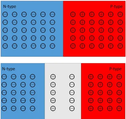
In a p-n junction, there are two different doped types of a semiconductor material involved. There is a p-type semiconductor with an excess of holes, together with an n-type semiconductor with an excess of electrons [20]. In the case of Silicon (the most conventionally used semiconductor material in IC design as well as for solar cells), the excess of electrons and holes in the semiconductor is achieved by adding Boron, Allumium, Nitrogen, Gallium or Indium for p-type and Phosphorous, Arsenic, Antimony, Bismuth or Lithium for n-type. There are also alternative semiconductor materials that enable the formation of p-n junctions such as Gallium Arsenide or Cadmium Telluride.
[image:30.595.176.382.409.603.2]
Fig. 1.1. Schematic diagram of a p-n junction. a) without depletion region. b) with depletion region.
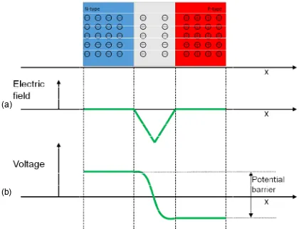
respectively near the interface
the generation of an Electric (E) field that opposes this diffusion as shown in Fig. 1.2 a [23]. As a consequence, the generated E field and the diffusion processes reach the equilibrium state
[image:31.595.103.523.221.543.2]the carriers are depleted which means that there are no free carriers available near the interface. For this reason, the region near the interface is called as the depletion region.
Fig. 1.2. 1D diagrams of a p
The presence of the depletion region leads to a potential difference across the junction as shown in Fig. 1
potential barrier for the remaining free electrons and holes on
semiconductor [23]. The selection of the right doping material is very important for the performance of p
width of the depletion region is (which is defined by the semiconductor materia and hence, how high the potential barrier is. Any carrier with a potential which is (a)
(b)
29
respectively near the interface [23]. The diffusion of electrons and holes lea of an Electric (E) field that opposes this diffusion as shown in
As a consequence, the generated E field and the diffusion processes reach the equilibrium state as shown in Fig. 1.1 b
s are depleted which means that there are no free carriers available near the interface. For this reason, the region near the interface is called as the
. 1D diagrams of a p-n junction under equilibrium state. (b) Voltage.
The presence of the depletion region leads to a potential difference across the as shown in Fig. 1.2 b. Therefore, the depletion region acts as a potential barrier for the remaining free electrons and holes on
[23]. The selection of the right doping material is very important for the performance of p-n junction. The doping level can adjust how large the width of the depletion region is (which is defined by the semiconductor materia and hence, how high the potential barrier is. Any carrier with a potential which is
[23]. The diffusion of electrons and holes leads to of an Electric (E) field that opposes this diffusion as shown in As a consequence, the generated E field and the diffusion b [23]. As a result, all s are depleted which means that there are no free carriers available near the interface. For this reason, the region near the interface is called as the
n under equilibrium state. (a) Electric field.
lower than the potential barrier at the depletion region cannot diffuse to the opposite type. More information about the p
will be provided in the discussion of Section 1.3.1.4.
Figure 1.1 b illustrates the p
region. This scenario is called equilibrium state [23]. However, the equilibrium state can be altered by applying an external voltage across the p
this case, the free electrons and holes can diffuse only if its potential is larger than the potential barrier across the junction. The value of the external voltage to be applied may vary with the material used. This value is known as threshold voltage. In the case of Si it is 0.7 V
voltage applied can vary the operation of the p operate either in forward or reverse
following sections [20, 23].
1.3.1.1 Forward biased p-n junction
Fig. 1.3. Schematic of a p
Figure 1.3 presents in a schematic the forward biased operation set up of a p junction. The p-n junction is considered in forward bias operation when: the positive potential terminal of the external voltage is applied on the p semiconductor. In addition, the
voltage is applied on the n-type. Under this condition, the depletion region gets narrower [23]. This is due to the repulsion that the positive and negative terminals have on the positive and negative charges of
semiconductors respectively [23]. In this way the
30
lower than the potential barrier at the depletion region cannot diffuse to the opposite type. More information about the p-n junction in the case of solar cells
provided in the discussion of Section 1.3.1.4.
Figure 1.1 b illustrates the p-n junction after the formation of the depletion region. This scenario is called equilibrium state [23]. However, the equilibrium state can be altered by applying an external voltage across the p-n junction. In free electrons and holes can diffuse only if its potential is larger than the potential barrier across the junction. The value of the external voltage to be applied may vary with the material used. This value is known as threshold i it is 0.7 V [24]. Moreover, the sign of the external voltage applied can vary the operation of the p-n junction. The p-n junction can operate either in forward or reversed bias which will be discussed i
n junction
Schematic of a p-n junction on forward biased operation
presents in a schematic the forward biased operation set up of a p n junction is considered in forward bias operation when: the positive potential terminal of the external voltage is applied on the p semiconductor. In addition, the negative potential terminal of the external
type. Under this condition, the depletion region gets narrower [23]. This is due to the repulsion that the positive and negative terminals have on the positive and negative charges of the p-type and n semiconductors respectively [23]. In this way the ability to diffuse increases lower than the potential barrier at the depletion region cannot diffuse to the
n junction in the case of solar cells
n junction after the formation of the depletion region. This scenario is called equilibrium state [23]. However, the equilibrium n junction. In free electrons and holes can diffuse only if its potential is larger than the potential barrier across the junction. The value of the external voltage to be applied may vary with the material used. This value is known as threshold [24]. Moreover, the sign of the external n junction can d bias which will be discussed in the
n junction on forward biased operation.
1.3.1.2 Reverse biased p
Fig. 1.4. Schematic of a p
Figure 1.4 presents in a schematic the reverse biased operation set up of a p junction. The p-n junction is considered in reversed bias operation when: the positive potential terminal of the external voltage is applied on the n semiconductor. In addition, the
voltage is applied on the p
depletion region gets wider [23]. This is due to the attraction that the positive and negative have on the positive and negative charges
type semiconductors respectively [23]. In this way the decreases.
1.3.1.3 I-V Curve of a p
The biasing of the p
the voltage across the junction. Figure 1.5 curve for a basic
p-31
1.3.1.2 Reverse biased p-n junction
Schematic of a p-n junction on reverse biased operation
presents in a schematic the reverse biased operation set up of a p n junction is considered in reversed bias operation when: the positive potential terminal of the external voltage is applied on the n semiconductor. In addition, the negative potential terminal of the external voltage is applied on the p-type semiconductor. Under this condition, the depletion region gets wider [23]. This is due to the attraction that the positive and negative have on the positive and negative charges of the p
type semiconductors respectively [23]. In this way the
V Curve of a p-n junction
The biasing of the p-n junction has a direct effect on the current flowing and on across the junction. Figure 1.5 shows the current versus voltage
-n junction.
n junction on reverse biased operation.
presents in a schematic the reverse biased operation set up of a p-n n junction is considered in reversed bias operation when: the positive potential terminal of the external voltage is applied on the n-type negative potential terminal of the external type semiconductor. Under this condition, the depletion region gets wider [23]. This is due to the attraction that the positive of the p-type and n-type semiconductors respectively [23]. In this way the ability to diffuse
Fig. 1.5. Typical I
When the p-n junction is in reverse bias (i.e. V< the depletion region is sufficiently
p-n junction is very small as shown on Fig. 1.5
junction is increased to more than the threshold, the p to be in forward bias. In this case, the
decrease of the potential barrier for free carriers to diffuse. current starts to flow through the p
highlight that this current is exponentially dependent on the applied voltage.
1.3.1.4 Single junction solar cell
Fig. 1.6. Schematic of a single junction solar cell
The basic solar cell is a p-n junctio reversed biased and encapsulated
1 The encapsulation process protects the layers of the materials forming the solar cell from rain, dust, extreme temperatures and moisture and it is carried out for all commercial solar cells. The encapsulation process is very important since it may affect
32
Typical I-V curve of p-n junction diode [25].
n junction is in reverse bias (i.e. V<0), the potential barrier due to sufficiently large. Hence, the current flowing through the very small as shown on Fig. 1.5. As the voltage across the p junction is increased to more than the threshold, the p-n junction is considered
bias. In this case, the depletion region reduces that leads to a decrease of the potential barrier for free carriers to diffuse. As a consequence, current starts to flow through the p-n junction. Additionally, it is imp
current is exponentially dependent on the applied voltage.
1.3.1.4 Single junction solar cell
Schematic of a single junction solar cell.
n junction as shown in Fig. 1.6. This p-n ju
ed and encapsulated1 to minimize any performance degradation
The encapsulation process protects the layers of the materials forming the solar cell from rain, dust, extreme temperatures and moisture and it is carried out for all commercial solar cells. The encapsulation process is very important since it may affect the life time of the solar cell.
0), the potential barrier due to large. Hence, the current flowing through the . As the voltage across the p-n is considered depletion region reduces that leads to a As a consequence, . Additionally, it is important to current is exponentially dependent on the applied voltage.
n junction is degradation
[image:34.595.134.409.489.637.2]33
due to adverse weather conditions. When the light is incident on the surface of a solar cell, part of it penetrates into the solar cell and the rest is reflected back to the air. In the ideal scenario all that light that has penetrated into the solar cell reaches the active layer (depletion region). The creation of electron-hole pairs, via the photovoltaic effect, takes place at this layer. Then, the electrons go to the positive contact and flow through the external circuit. Hence, a photo generated current is produced. However, the ideal case is not possible due to performance limitations caused by material properties such as the band gap of the material (discussed later in this section). As a consequence it is necessary to characterize the solar cell performance. Additionally, there are several quantities that are helpful in understanding whether or not the solar cell performs as required. These parameters can be representative of the optical or of the electrical performance of the device. A brief introduction about the most meaningful parameters is presented below.
Characterization of optical properties:
Reflection (R) [23]:
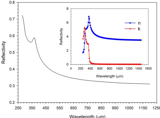
This parameter gives the amount of light that the solar cell reflects from the surface. In the case of Si solar cells, at the interface between air and Silicon, there is a large refractive index difference between the two materials [26]. This difference leads to high reflection from the interface of an incident wave [26]. The waves that are reflected can be predicted at normal incidence by Fresnel’s equations [27, 28] (given the dispersive refractive index of the material) as follows:
2 2
2 2
n 1 k
Reflectivity
n 1 k
(1.1)
34
Fig. 1.7. Reflectivity vs. wavelength curve from the planar air-Silicon interface. Inset 1 real and imaginary parts of the refractive index of Si.
Figure 1.7 shows clearly how large the reflection from the air-Silicon interface is. This means that the amount of light reaching the absorbing layer of a Si solar cell is highly dependent on the refractive index difference at this interface. If the reflection at this interface can be reduced, it would mean that more light reaches the active layer, increasing chances of absorption. There are various means available to increase the transmission into the Si such as: anti reflection coating or trapping the light to increase the light path which will be discussed in Section 1.5. Reducing the reflection from the solar cell is the main target of the work presented in this thesis.
Absorption
A
[23]:photon absorption leading to the transition of electron bands, has to obey the conserv
where k , k , Ei f i
photon momentum, the initial associated energy with the photon and the final associated energy with the photon respectively. The photon momentum
and the associated energy are represented by
Either direct or indirect band gap semiconductor can b
[image:37.595.127.545.394.548.2]Figure 1.8 presents the transition of an electron upon the arrival of a photon for direct and indirect band gap:
Fig. 1.8. Schematic of electron transition for
- Direct band gap semiconductor: In this type of material, the transition of electrons from valence to conduction band is direct (i.e. the minimum energy level of the
maximum e
occur, the photon is not required to carry any momen the momentum [30
energy higher
Arsenide (GaAs) is one of the most studied direct band gap materials for solar cells
(a)
35
photon absorption leading to the transition of electron
bands, has to obey the conservation of energy and momentum [30
i f
k q k
i f
E
E
i f i
k , k , E and
E
f are the initial electron momentum, the electron photon momentum, the initial associated energy with the photon and the final associated energy with the photon respectively. The photon momentumand the associated energy are represented by
q
andEither direct or indirect band gap semiconductor can be used in this layer. presents the transition of an electron upon the arrival of a photon for direct and indirect band gap:
Schematic of electron transition for. a) direct and. b)
Direct band gap semiconductor: In this type of material, the transition of electrons from valence to conduction band is direct (i.e. the minimum energy level of the conduction band is aligned with the maximum energy level of the valence band [30]). For the transition to occur, the photon is not required to carry any momen
the momentum [30]. This leads to high absorption of photons with energy higher than the energy band gap of the device. Gallium Arsenide (GaAs) is one of the most studied direct band gap materials for solar cells [31]. However, there are also reports describing the
(b)
photon absorption leading to the transition of electron between energy ation of energy and momentum [30]:
k q k (1.2)
(1.3)
are the initial electron momentum, the electron
photon momentum, the initial associated energy with the photon and the final associated energy with the photon respectively. The photon momentum
q
and respectively.e used in this layer. presents the transition of an electron upon the arrival of a photon
b) indirect band gap.
36
properties of other direct band gap materials such as: Gallium Selenide (GaSe) [31].
The absorption coefficient associated with this type of semiconductors is as follows [32]:
12 ph g
h A E E
(1.4)
Where , Eph,Eg and A are absorption coefficient, photon energy,
energy band gap and a direct band gap material constant respectively.
- Indirect band gap semiconductor: In this type of material the transition of electrons from valence to conduction band is indirect (i.e. the minimum energy level of the conduction band is not aligned with the maximum energy level of the valence band [30]). Therefore, for the transition of the electron to take place the photon must carry sufficient momentum to satisfy the momentum conservation Eq. (1-2) [30]. This reduces the chances of photon absorption since not all incident photons with energy higher than the energy band gap of Silicon (i.e. 1.1 eV) are absorbed. Nevertheless, photons with energy higher than 3 eV in Silicon can lead to a direct transition. Examples of other indirect band gap materials are: Germanium (Ge) or Gallium Phosphide (GaP).
The absorption coefficient associated with this type of materials is as follows [32]:
h B Eph Eg 2 (1.5)
Where , Eph,Eg and B are absorption coefficient, photon energy,
37
In the solar cells, a direct band gap material is preferred. Devices with direct band gap materials on their active layer are likely to have high conversion efficiencies. However, Silicon which is an indirect band gap material (very abundant on Earth and non-toxic) is the most popular active material in the solar cell industry. This is due to the influence of the IC design industry (Silicon based). This influence led to a strong development of solar cell devices based on Silicon until the limitations of Silicon for photovoltaics were identified. Since then, scientists have tried to improve the performance of devices with direct band gap materials to experimentally compete with those solar cells made of Silicon. The band energy profile needs to match better with the solar spectrum and a direct transition should enable a thinner active layer (reducing costs). A more detailed explanation on the consequences and possible solution will be discussed in Section 1.3.
Characterisation of electrical properties:
Recombination [23, 33, 34]:
This parameter represents the phenomenon by which electron-hole pairs generated via the photovoltaic effect separate without contributing to the photo current. In a solar cell it is required to control it since it can severely alter the energy conversion. The challenging process of surface passivation can help to reduce the negative effects of recombination on the performance. There are various types of recombination:
38
- Auger: It is a type of non-radiative recombination. The difference lies in how the electron is excited to a higher energy state. In this case when an electron-hole pair recombines, there is no emission of a photon or heat as in non-radiative recombination. However, in this case the energy is transferred to an electron which is in the conduction band and then is excited to a higher energy state [20].
- Radiative: An electron for the conduction band bonds with a hole on the valence band. From this combination a photon is emitted with energy similar to the band gap of the material. This process is very frequent in direct band gap materials. In the case of solar cells with indirect active material such as Silicon, it can be neglected.
Open circuit voltage
V
OC [23]:This is the voltage across the solar cell when it is not connected to any external circuit. This is the maximum voltage that the solar cell is able to produce. Therefore, the Voc value largely affects the performance of the solar cell.
However, under this condition there is no current flow and hence there is no power delivered. The higher the value of the open circuit voltage the lower radiative recombination is. Hence, Voc is an indicator of the recombination level of the solar cell. Furthermore, Voc is dependent on the photogenerated current density and the saturation current. This is due to the open circuit voltage dependence on the radiative recombination that takes place in the device. Furthermore, the Voc is closely related to the energy band gap of the material since the larger the band gap the higher the Voc.
Short circuit current
I
SC [23]:39
short circuit current density, during the developing stage, is done using a standard solar spectrum. The solar spectrum that is conventionally used in the field of solar cells is known as the AM 1.5 solar spectrum [36] (to be discussed in Section 2.3.7). The value obtained from measuring the current, while the terminals are short circuited, is the maximum current the solar cell is able to produce. Similar to VOC there is no power delivered. Under this
condition the voltage across the device is minimum. We want to have the short circuit current as high as possible to achieve a high power delivery when in operation.
Fill factor (FF) [23]:
The information provided by this parameter is how close the performance of the device (delivering maximum power) is to its ideal performance. The maximum power delivered by the solar cell will be achieved when the product of voltage and current delivered are maximum. The maximum value of voltage(V ) is achieved only when the current is minimum and the OC
maximum current delivered (I ) is achieved only when the voltage is SC
minimum. In the cases where either voltage or current are prioritised for a specific application, there is a trade-off between current and voltage. This trade-off will have an impact on the maximum power delivered and hence lower the FF value. This is a key factor that shows the ratio between the maximum power available from the solar cell and ideal maximum power of the device. The idea is to have a Fill Factor as close to ideal as possible (i.e. 1).
MP MP
OC SC
V *I FF
V *I (1.6)
Where VM P is the voltage at maximum power and IMP is the current at
maximum power.
Conversion efficiency
[23]:40
case. This means, in the ideal case where all the incident photons on the solar cell contribute to current generation.
SC OC
IN
J * V * FF
P (1.7)
Where P is the power of the incoming light. IN
These optical and electrical properties may be affected also by external parameters. Some of these parameters and their consequences are introduced as follows:
- Temperature: When there is light incident on the solar cell, part of the energy from the photons, with energy higher than the band gap (please refer to the discussion on basic solar cell), is liberated as heat. Investigations on the effect of increasing operating temperature of solar cells have reported a lower output power as well as lower conversion efficiency [37]. An approach to reduce the unwanted effects is to extract the heat by cooling down the solar cell [38]. This can be done by using photovoltaic thermal collectors [38].
41
- Moisture: As solar cells approach the end of their life time, the probability of moisture inside the solar cell increases. However, this problem can also be present at any moment through the solar cell life time. It is due to the failure of the encapsulation of the solar cell (every commercial solar cells is encapsulated). In this scenario, the mobility of electrons and holes decrease [41]. Furthermore, in some cases there is even a delamination of each individual layer [41]. The best solution to minimise the presence of moisture is to take extra care while encapsulating the solar cell.
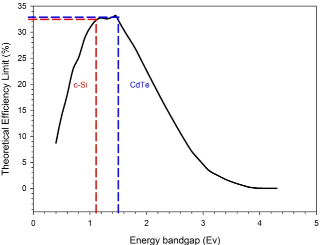
In addition to these parameters there are other internal parameters severely affecting the performance of the solar cell. These parameters were reported to limit the efficiency of solar cells. This limit is known as Schockley-Queisser limit [42] which is discussed in the following section.
1.3.1.5 Schockley-Queisser limit
42
Fig. 1.9. Efficiency vs. Energy band gap of the active material according to the detailed balanced analysis presented by Shockley and Queisser [42].
From Fig. 1.9 it is possible to see the result of the detailed balance. The theoretical maximum efficiency is shown for a range of Energy band gaps. In the case of Si (the most popular active material for solar cells) the 1.1 eV energy band gap leads to an efficiency limit of ≈ 33% as shown in Fig. 1.9. Since this efficiency limit was reported, to overcome it has become the target of many researchers. However, for a single junction Silicon solar cell the conversion efficiency still has not reached the limit. The highest efficiency for this type of solar cell is reported to be 25.6 % [18, 19]. Some researchers have tried to use absorbing materials different from Silicon such as GaAs [43-45]. Others have tried to increase the number of junctions and even concentrate the sunlight onto a multijunction solar cell. In the next section, multijunction solar cells are discussed.
1.3.2 Multijunction solar cells
43
a single junction solar cell, there is only one absorbing material generating one electron-hole pair per photon absorbed. This happens only when the energy of the incident photon is larger than the energy bandgap of that material. When the energy of the photon is larger than the bandgap, the same number of electron hole pairs is liberated. The excess energy is liberated as heat [48]. Hence, the extra photon energy does not contribute to generate more photocurrent. Alternatively using multijunction solar cells to optimize the solar spectrum can improve the impact of high energy photons. Multijunction solar cells enable different wavelength ranges of the solar spectrum, to be absorbed in different active layers [49].
44
this five junction solar cell were 4.78 V, 12.0 mA/cm2 and 83.5 % respectively [18, 52]. These values show how well a multijunction solar cell can perform.
However, even if there are many advantages of using this type of solar cells, their use is limited to specific scenarios. This is due to the higher costs associated with the fabrication techniques required [1]. For example, it is possible to see this type of solar cell in aerospace applications [1]. In terrestrial applications, currently multijunction solar cells are limited in use for concentrated solar cells [53] (to be discussed in Section 1.3.5). The most popular solar cells have crystalline silicon (c-Si) as the active material which are discussed in the following section.
1.3.3 Crystalline Silicon solar cells
Among all solar cell technologies, c-Si solar cells enjoy the largest market share (~90%) [23]. In addition, this type of solar cells is normally known as “traditional” solar cells and first generation solar cells [1]. Silicon is a material widely available on Earth and it is not a contaminating material [54]. The first solar cell in 1950s was made using this technology and there has been a massive development since then [5]. That is partially due to the influence of the integrated circuits industry. The good understanding on Silicon properties for bipolar junction transistors enabled the development of Silicon for solar cells [1]. Currently, this type of solar cell holds the highest conversion efficiency on record for a single junction solar cell 25%, with Voc= 0.740 V, Jsc=41.8
2
mA cm giving FF=82.7% [18, 19]. In addition to this, as of 2013, it enjoyed
90% of the solar cell market share.
45
have developed new types of solar cells with thinner active layers [55]. In the next section, the most important thin film solar cells are discussed.
1.3.4 Thin film solar cells
Thin film solar cells discussed in this section are grouped as the second generation of solar cells. Many researchers found the development of this type of solar cells for achieving high efficiencies while reducing material costs as an attractive challenge [55]. Different thin film solar cells were tested but the following three types of solar cells were the most promising ones: amorphous Silicon (a-Si) solar cells, Cadmium Telluride (CdTe) solar cells and Copper Indium Gallium Selenide (CIGS) solar cells. In the following sections these types of solar cells are discussed, starting the discussion with a-Si solar cells.
1.3.4.1 Amorphous Silicon (a-Si) solar cells
Among the three types of solar cells mentioned above, a-Si solar cell has been developed faster than the others [1]. It is commonly found in calculators powered by solar power [56]. The active layer is a-Si which means that the active material does not have a crystal structure [55]. As a consequence, the absorption length of a-Si is shorter than that of crystalline Silicon [57]. It results in better photon absorption which enables a thin active layer with energy bandgap 1.75 eV [58]. There are other advantages of using a-Si such as: it is an abundant and non-toxic material, has capability for large scale production and a low temperature growing process [58].
46
has limited the applications of this type of solar cells despite the extensive research on the area [1]. The effect of the photodegradation can be reduced by using a thinner layer. However, a thinner layer reduces absorption requiring optical confinement complicating the process. The highest efficiency recorded
for this type of solar cell is 10.2% with Voc= 0.896 V, Jsc=16.39 mA cm giving 2
FF=69.8% [58]. The photodegradation and the conversion efficiency, lower than traditional solar cell, made researchers to continue the search for new active materials [58]. In the following section CdTe solar cells are discussed.
1.3.4.2 Cadmium Telluride (CdTe) solar cells
Cadmium Telluride (CdTe) is a material which has a bandgap of 1.5 eV [58]. This is close to the theoretical value considered as ideal for high conversion efficiency [61, 62]. From Fig. 1.9 it is possible to identify that 1.45 eV is the ideal band gap to satisfy the theoretical maximum efficiency of 33% predicted by Schokley and Queisser [62]. The absorption coefficient of this material is
10 cm in the visible region [58]. This means that for the active layer 5
thickness to absorb 90% of the arriving photons only few micrometres are required [58]. The theoretical efficiency for this type of solar cells oscillates between 28% and 30% [58, 63-65]. However, the efficiencies achieved are far from this value. In optimum conditions, in an experimental lab, CdTe solar cells have been reported to reach 21% energy conversion efficiency [18, 66]. This
optimum solar cell has Voc= 0.8759 V, Jsc=30.5 mA cm giving FF=79.4% 2
[66]. The technology involved in the fabrication process of CdTe solar cells is has developed very fast in the last decades [67]. Nowadays the improvement in the field is mainly limited to the improvements recorded by First Solar [68]. Nevertheless, the expectations for further improvements are still high due to the state of the technology involved in the fabrication of CdTe solar cells [68]. It is possible to achieve solar cells with efficiency higher than 10% by applying several manufacturing methods. This is promising for the future of this technology since it indicates low dependence on a single fabrication procedure.
47
is harmful to the health of human beings [1, 69]. In Europe some countries are concerned about the health and environmental impact [70]. However, there are researches that claim a low risk of environmental impact when CdTe solar cells are placed in residential areas on rooftops [1]. In any case, caution must be taken when recycling all the components of the solar cell [71]. Currently there are companies manufacturing solar cells using this technology. The market share of this type of solar cells is growing but it is small still compared with other technologies. The market share for CdTe solar cell is recorded to be 6% as of 2007 [72]. This is due to lower conversion efficiencies than traditional Silicon solar cells. In the following section CIGS solar cells are discussed.
1.3.4.3 Copper Indium Gallium Selenide (CIGS) solar cells
Copper Indium Gallium Selenide solar cells have the potential of low processing cost. It is a direct bandgap material with energy bandgap 1.53 eV which enables a thin active layer [58]. In addition, there is no polluting component involved in this technology [55]. Further, there is no evidence showing that it is harmful to human beings [55]. Moreover, it offers the possibility of flexible solar cells. This is a very promising characteristic since it enables integrating solar cells into new buildings. In terms of fabrication processes, it introduces the option of the so called roll-to-roll approach. It represents a much simpler manner to mass produce this type of solar cells. The highest energy conversion efficiency reported for this technology is 21% [18, 73]. The Voc of this solar cell is 0.757 V and Jsc is 35.70 mA/cm2 giving a fill factor of 77.6% [73].
48 1.3.5 Concentrated solar cells
[image:50.595.94.449.327.564.2]The difference between conventional solar cells and concentrated solar cells lies in a system that focuses the incident sunlight onto a specific point [1, 47]. A small multijunction solar cell is generally placed on this point. The small size compared to non-concentrated solar cells allows the usage of highly efficient and more expensive cells. Figure 1.10 presents a concentrated solar cell with the mirrors focusing the light on the multijunction solar cell [53]. In this way the intensity of the light reaching the solar cell is very high [76]. Since the intensity of the light increases, the chances of absorbing a photon increases as well. Hence, the conversion efficiency of concentrated solar cell increases when compared with non-concentrated solar cells.
Fig. 1.10. Typical concentrated solar cell [77].
49
79]. This device would keep as constant as possible the angle between the solar cell and the sun. Hence, it is ensured that the position of the mirrors would allow for maximum concentration. There are different types of tracking systems:
- Single axis tracking system: This tracking system can only rotate the solar cell in one direction to follow the trajectory of the sun [80].
- Two axes tracking system: This tracking system can rotate in two directions. These directions are normally perpendicular to each other. Hence, it is possible to track the trajectory of the sun more accurately [81].
Up to now, the highest efficiency has been reported for concentrated solar cell systems with a value of 46% [82]. These systems require a high maintenance due to the tracking systems required for optimum operation [47]. This turns into a high cost for installing concentrated solar cells even though the costs have reduced significantly [83]. In 2013, the costs of installing solar cell power plants for 10 MW were within the range of 1400 €/KW and 2200 €/KW [83, 84]. Moreover, the concentration of the sunlight onto the multijunction solar cells leads to overheating the device [1]. This can deteriorate the performance of the solar cell unless cooling systems are deployed to reduce the temperature [85]. In the following section solar cells made of organic materials are discussed.
1.4 Organic solar cells
Organic solar cells are considered to be in the group of third generation solar cells. When researchers started to work on organic solar cell the expectations were: high efficiency, thin solar cell, flexibility, integration on buildings and easy mass production process, etc. [1, 47, 86]. The absorption coefficient of organic materials is larger than the absorption coefficient of inorganic solar cells. In the
50
[image:52.595.138.407.180.348.2]than the energy required to fabricate a traditional solar cell [86]. Furthermore, flexible organic solar cells can be achieved thanks to the usage of new materials. This can stimulate the integration of solar cells when making new buildings [47]. Furthermore, the fabrication process is simpler than the fabrication process for inorganic solar cells.
Fig. 1.11. Schematic of a bulk-heterojunction solar cell [89].
51
This process involves many challenges, such as the diffusion length of the exciton being very short [86]. This implies that while the exciton diffuses towards the acceptor it can recombine; not contributing to the photocurrent [91]. A solution to overcome this is the adoption of the bulk-heterojunction (see Fig. 1.11 for reference) which mixes up both donor and acceptor materials [86]. As a result, the exciton does not need to travel a long distance to reach the acceptor.
Organic solar cells have a great promising feature of flexibility which may enable solar cells to be used in future applications, such as: built-in in new buildings or in clothing, etc. However, the efficiency of organic solar cells is much lower than for inorganic solar cells. The best conversion efficiency achieved for an organic thin film solar cell is 11% with Voc 0.739 V,
sc
J 19.40 mA/cm2 and FF 71.4 % [92]. Hence, organic solar cells do not have a large market share. Their market share in 2013 was recorded as 1.5% [93]. In recent years the focus has been on new type of solar cells combining both inorganic and organic active layers [94]. They are called perovskite solar cells and are discussed in the following section.
1.4.1 Inorganic-Organic Perovskite solar cells

![Fig. 1.5. Typical ITypical I-V curve of p-n junction diode [25].](https://thumb-us.123doks.com/thumbv2/123dok_us/1402657.93259/34.595.134.409.489.637/fig-typical-itypical-i-v-curve-junction-diode.webp)

![Fig. 1.10. Typical concentrated solar cell [77].](https://thumb-us.123doks.com/thumbv2/123dok_us/1402657.93259/50.595.94.449.327.564/fig-typical-concentrated-solar-cell.webp)
![Fig. 1.11. Schematic of a bulk-heterojunction solar cell [89].](https://thumb-us.123doks.com/thumbv2/123dok_us/1402657.93259/52.595.138.407.180.348/fig-schematic-bulk-heterojunction-solar-cell.webp)