High-Frequency EMI Attenuation at Source with the
Auxiliary Commutated Pole Inverter
Apollo Charalambous, Xibo Yuan,
Senior Member, IEEE,
and Neville McNeill
Abstract—Fast-switching power converters are a key enabling technology for the More Electric Aircraft (MEA), but the generated Electromagnetic Interference (EMI) poses significant challenges to the electrification effort. To meet the stringent aerospace EMI standards, passive filters are commonly employed, despite the weight and size constraints imposed by the MEA. Alternatively, the EMI source, i.e., the high dv/dt and di/dt slew rates, can be addressed through waveform-shaping techniques. For example, while most soft-switching converters can reduce switching loss, they do so by switching the semiconductor devices in a slower and smoother manner, resulting in the attenuation of high-frequency harmonics. This paper examines the Auxiliary Commutated Pole Inverter (ACPI) topology, and its first contribution is the attenuation of the high-frequency content of its EMI source, that is, the output voltage, in a predictable manner, through the active control of the resonant circuit. This is achieved by firstly discussing the time-domain characteristics of trapezoidal and S-shaped pulse-trains that lead to attenuated high-frequency harmonic content, and secondly, by analysing the equivalent LC circuit of the ACPI. The design of the inverter is then focused on the active control of the resonant parameters, for a predetermined and enhanced output voltage high-frequency response. The second contribution of this paper is the comparison of the EMI performance of hard switching and of three soft-switching modes, fixed-timing control, variable-timing control, and capacitive turn-offs, and how this informs important metrics like power efficiency, current stress, and implementation complexity. Lastly, the third contribution is on the trade-offs that arise when the primary design goal is enhanced EMI performance, as opposed to switching loss reduction. A 5-kW, 3-phase ACPI prototype is used for validating the high-frequency content attenuation at source. It is shown that the ACPI can achieve a 37-dB harmonic attenuation of its output voltage at 4 MHz, compared to a hard-switched inverter.
Index Terms—Auxiliary commutated pole inverter; EMI; fixed timing; frequency response; more electric aircraft; soft switching; variable timing.
I. INTRODUCTION
Power electronic converters play a crucial role in the electrification of vehicles and aeroplanes. For example, they are among the key enabling technologies for the More Electric Aircraft (MEA) [1], where electrical systems are increasingly adopted for replacing actuation, fuel handling and cabin air pressurisation systems traditionally powered through hydraulic,
pneumatic and mechanical means. MEA offers significant potential for reducing aircraft energy consumption, and consequently, for decreasing fuel burn and emissions. With on-board electrical power generation capacity reaching 1.5 MVA for new aircrafts and future forecasts showing an upward trend with electric propulsion, aggressive power density and efficiency targets are being set for new power electronic equipment to be installed, e.g. 15 kW/kg for power density and 95%+ for efficiency. For these goals to be achieved, the switching speed is pushed higher and higher for reducing the switching loss, thus improving the efficiency and reducing the cooling requirements, e.g. with the use of wide-bandgap power devices [2]. The switching frequency is also being increased for reducing the size of the passive components, such as filtering inductors and capacitors, and for improving the power density.
However, the fast switching action of power devices such as IGBTs and MOSFETs causes high-frequency Electromagnetic Interference (EMI) [3]. This is a major disadvantage, because EMI may disrupt the operation of surrounding electronic equipment [4,5]. Furthermore, common-mode EMI (CM EMI) from voltage-source converter (VSC) based motor drives can cause motor premature winding failure, ball bearing deterioration, and motor terminal overvoltages [6-8]. The electrification effort will thus be hindered if EMI remains unchecked. This is why the aerospace industry has stringent EMI standards such as the DO-160 [9] that defines the limits of conducted EMI in the range between 150 kHz and 152 MHz. The low-frequency EMI, i.e. from 150 kHz to 1 MHz is normally driven by PWM-associated harmonics and the high-frequency EMI from 1 MHz to 152 MHz is mainly driven by the switching transitions and the associated dv/dt and di/dt rates.
Conducted EMI is usually attenuated with the help of passive filters [3,10]. However, filters can add a significant portion to a converter’s weight and size. This negates the effort to save weight and space that is pursued by the MEA concept, and increases overall cost as well.
Instead of adding filters, the EMI emissions can be attenuated at source. For low-frequency PWM-driven EMI (150 kHz to 1 MHz), this can be achieved by using specialised modulation schemes like common-mode voltage cancelling [11] and random/chaotic switching [12], or even a lower switching frequency. For high-frequency switching transient-driven EMI (1 MHz to 152 MHz), solutions include the shaping of the converter/power device waveforms such as through active gate driver control of the power devices [13], and the use of soft-switching topologies. The active gate driver control method is not pursued in this work since the complexity of such circuits
A. Charalambous and X. Yuan are with the Department of Electrical and Electronic Engineering, University of Bristol, Bristol BS8 1UB, U.K. (e-mail: [email protected]; [email protected]). Corresponding author: Xibo Yuan.
adds significant design effort, and the potential benefit of reducing both switching loss and EMI emissions is not possible. As it is known, soft-switching topologies are commonly used for switching loss reduction by decoupling the transitioning edges of the current and voltage of the semiconductor devices [14,15,16]. This decoupling is usually realised with LC circuits that slow and smooth the edges in a resonant manner. When the voltage is manipulated like this, zero-voltage switching (ZVS) is performed. When the current is, zero-current switching (ZCS) is realised. Therefore, the switching transition can be effectively profiled with the di/dt and dv/dt rates controlled by the resonant circuit. As such, soft-switching converters are promising in reducing switching loss as well as the high-frequency content of the switching magnitudes. This is the main reason why soft switching is pursued in this paper.
Though there is a multitude of papers discussing topologies, modulation and control of soft-switching converters, the focus is on reducing the switching loss rather than EMI attenuation. In contrast, works such as [17-22] do indeed explore the viability of reducing EMI with soft-switching converters, both in simulation and in experiment, with encouraging results. An experimental 50-kW, 3-phase auxiliary commutated pole inverter (ACPI) prototype exhibits a 10-dB drop in conducted emissions in the 3 to 5 MHz range and a 5-dB drop from 8 to 12 MHz when compared to an equivalent hard-switched inverter [17]. In [21] a 70-W ZCS flyback converter exhibits a 16-dB conducted EMI attenuation in the frequency range of 5 to 20 MHz, when compared to its hard-switched counterpart. In these papers, it is recognized that some soft-switching topologies showcase an enhanced EMI performance because the di/dt and dv/dt slew rates are influenced directly by the soft-switching process. However, high-frequency harmonic attenuation is treated merely as a by-product of soft switching, or at best, when EMI attenuation is actively pursued, only simulation and experimental results are presented with no insight as to how the resonant process can be actively controlled for this specific task. In contrast, the first contribution and the focus of this paper is a method of predetermining and attenuating the high-frequency content of an EMI source through the active control of the resonant circuit. The important time-domain characteristics of pulse-trains that lead to less high-frequency content are explored, and inform the design of a soft-switching converter for exhibiting an enhanced frequency response. This is done through analytical expressions for both the high-frequency response and the resonant circuit magnitudes. For this study, the auxiliary commutated pole inverter (ACPI) is chosen, a PWM-compatible soft-switching topology that highly resembles the VSC topology. VSCs are the industry standard in variable-speed motor drives, such as the Engine Starter Motor used for jet engine start-up on MEAs [1,23]. Therefore, the ACPI can be easily employed in motor drive applications.
The developed high-frequency attenuation method is based on the active control of the ACPI’s resonant circuit for reducing the harmonic content of the output voltage, which is a significant source of EMI in VSCs. At the heart of this resonant circuit lies an equivalent series LC circuit, the study of which forms the basis for the second contribution of this paper, namely the development and comparison of three ACPI soft-switching control schemes: fixed timing, variable timing, and capacitive turn-offs. The high-frequency response of these soft-switching schemes is discussed in depth, as well as how inevitably, the demand for attenuated harmonic content informs their performance regarding current stress, power efficiency, and
implementation complexity. For example, while capacitive turn-offs can reduce current stress and auxiliary circuit loss by bypassing the auxiliary circuit, they generate linear output voltage edges that can potentially increase the high-frequency harmonics. Therefore in this paper, for the purpose of generating of an output voltage with only sinusoidal edges, capacitive turn-offs are initially ignored. All these trade-turn-offs are also studied for the hard switching mode. Lastly, the third contribution of this work is on the trade-offs that arise when the ACPI is designed primarily for enhanced EMI performance, as opposed to when it is designed primarily for switching loss reduction.
This paper is structured as follows: Section II describes the operation of the ACPI. Section III presents the frequency response of trapezoidal and S-shaped pulse-trains, as the basis for an ACPI output voltage with attenuated high-frequency content. Section IV analyses the equivalent LC circuit, and explains how its resonant parameters, specifically the ‘boost’ currents, can actively control the duration and smoothness of the output voltage edges. Section V discusses and compares the fixed- and variable-timing control schemes with regards to implementation complexity, current stress, power loss, and crucially, output voltage edge shaping. Section VI details the ACPI design procedure for attaining an output voltage with attenuated high-frequency content. Lastly, Section VII presents the experimental results of the high-frequency attenuation, power efficiency, switching transients, and other special issues regarding the operation of the ACPI.
II. THE AUXILIARY COMMUTATED POLE INVERTER A. Auxiliary Resonant Pole Inverters
This work primarily addresses high-frequency content attenuation at source for the VSC as an AC/DC rectifier, or a DC/AC inverter for motor drives in electromagnetically sensitive environments like the MEA, where it is imperative that the dv/dt of the output voltage is reduced [24]. The 6-switch, 2-level, 3-phase VSC is the standard configuration for AC/DC or DC/AC power conversion. Thus application-wise, the considered soft-switching topologies should be similar to the standard VSC. Given the focus is on the output voltage dv/dt and profile, only ZVS inverters are considered.
The topologies with the highest degree of PWM compatibility, independent phase-leg control, and efficiency, that most resemble the VSC are the auxiliary resonant pole inverter (ARPI) family of ZVS inverters [25]. The most popular ARPIs are the coupled-inductor ZVS inverters [26-29], and the ACPI [30,31]. The coupled-inductor inverters are intended for adaptable control to any load level, and they exhibit the least amount of auxiliary circuit loss of all the ARPIs. However, they have a complicated design and high component counts. The ACPI on the other hand, might exhibit more auxiliary loss, but it has a lower component count, and its operation is simpler and more flexible. For this last reason, the ACPI is chosen as the subject of this study.
B. Operation of the ACPI
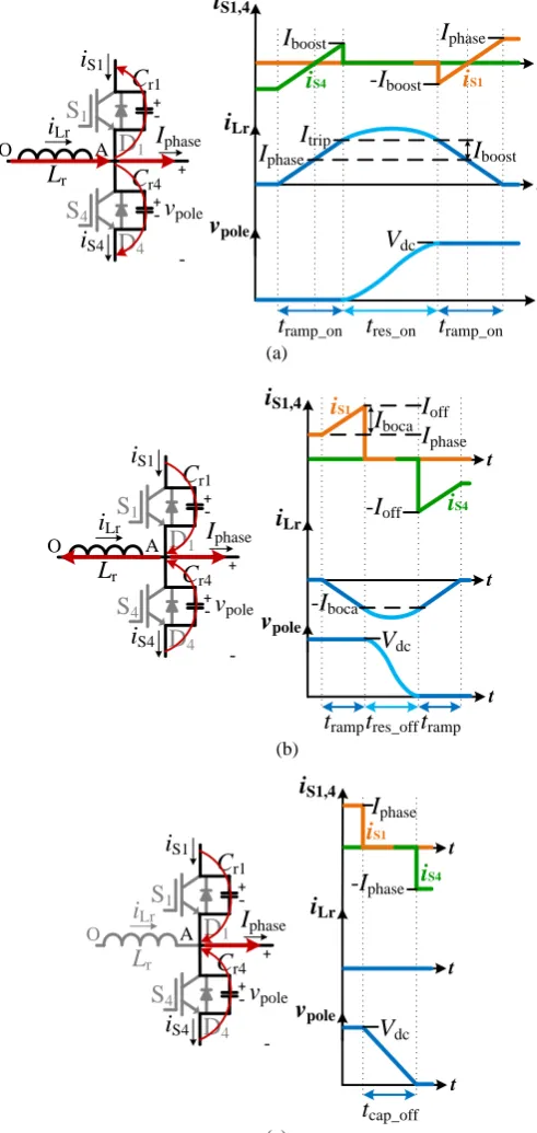
Fig. 1 shows an ACPI phase-leg, where a VSC phase-leg of main devices S1/D1 and S4/D4 is supplemented with an auxiliary
branch between the DC midpoint O and the output node A. This branch consists of auxiliary devices Sa1/Da1 and Sa4/Da4, in series
with a resonant inductor Lr. Cr1 and Cr4 are snubber capacitors
clamping diodes, though not part of the topology, are essential for protecting the auxiliary devices against overvoltages.
Fig. 2 shows the waveforms of the inductor current iLr, the
phase-leg output voltage vpole, and the switching currents iS1 and
iS4 of the main devices, during a switch turn-on transition (D4 to
S1) in Fig. 2(a), a switch turn-off transition (S1 to D4) in Fig. 2(b),
and a capacitive turn-off transition (S1 to D4) in Fig. 2(c). The
phase current Iphase is considered positive and constant during a
transition. The sub-circuits during each vpole transition are also
shown.
The turn-on transition of Fig. 2(a) starts with Sa1 turning on
first. During the tramp_on interval, iLr ramps up and Lr accumulates
energy. As iLr surpasses Iphase, iS4 reverses through S4. Then, iLr
reaches Itrip and iS4 reaches Iboost. At this point, Lr starts resonating
with Cr1 and Cr4. During the resonant interval tres_on, vpole
sinusoidally swings from the negative to the positive rail until it is clamped by D1. Then iLr starts ramping down, and the
incoming S1 is gated on. As soon as iLr drops below Iphase, S1
starts conducting. It is seen that a resonant turn-on transition always involves a swap between the antiparallel diode and its switch, as attested by the direction reversal of iS4 and iS1. The
swap from D4 to S4 allows for the controlled triggering of
resonance, and a grace period is created as D1 conducts during
which S1 is turned on under ZVS.
The turn-off transition of Fig. 2(b) starts with Sa4 turning on
first, and iLr ramping down in the negative direction, during the
tramp_off interval. Meanwhile, the outgoing switch S1 conducts the
sum of iLr + Iphase. When iLr reaches the value of Iboca, and iS1 the
value of Ioff, S1 is turned off and resonance commences. During
the resonant interval tres_off, vpole swings down to the negative rail,
and the edge is shaped in a sinusoidal fashion. Then, the incoming D4 clamps vpole, S4 is gated on, and iLr starts ramping
up to zero. Steady state is then established with D4 conducting
Iphase.
The resonant process performs ZVS turn-on and turn-off of the main devices, and ZCS turn-on and natural turn-off of the auxiliary ones. The voltage and the current are decoupled, with resonance slowing down vpole and shaping it in a smooth,
sinusoidal manner. Hence, the ACPI can reduce switching loss, while profiling the dv/dt of vpole. However, with hard switching
no auxiliary circuit power loss exists [25,31]. Also, soft switching increases the current stress on the main devices, especially during the turn-off transition, because of the inductor current components Iboost and Ioff that are imposed on iS1 and iS4.
Hard switching though cannot perform waveform shaping and smoothing, like soft switching can.
The main device current stress caused by the resonant turn-off transition can be avoided when a capacitive turn-turn-off takes place, as seen in Fig. 2(c). Simply, Iphase alone discharges Cr4 and
charges Cr1, and vpole transitions in a linear rather than a resonant
manner, like a lossless turn-off snubber [14,32]. The auxiliary
circuit is not utilized, which avoids the auxiliary loss and the extra current stress on the main devices. However, a capacitive turn-off is possible only at sufficiently high Iphase levels.
Otherwise it will last too long, causing problems such as a current spike in the incoming device [33,34], and the drop of pulses if the PWM time constraints are violated.
In summary, the ACPI performs three kinds of transition: resonant switch turn-ons that occur during the entire fundamental cycle T1, resonant switch turn-offs, and capacitive
switch turn-offs. Resonant turn-off transitions can be utilized during the entirety of T1, or at high Iphase levels, they can be
replaced with capacitive ones. The way that each kind of transition occurs, influences the vpole high-frequency, as well as
the overall power loss and current stress of the ACPI.
A
S
1C
r1D
1I
phaseV
dc/2
v
pole +-S
4C
r4D
4P
O
N
+ -+ -+-V
dc/2
+-S
a4S
a1D
a1D
a4D
s4D
s1L
r [image:3.595.307.553.230.748.2]i
LrFig. 1. The circuit schematic of the ACPI phase-leg.
A
S
1C
r1D
1I
phasev
pole +-S
4C
r4D
4 + -+-L
ri
Lr t tI
phaseI
tripV
dcI
boostt
res_ont
ramp_ont
ramp_ont
i
S4i
S1 AS
1C
r1D
1I
phasev
pole +-S
4C
r4D
4 + -+-L
ri
Lri
S4i
S1 AS
1C
r1D
1I
phasev
pole +-S
4C
r4D
4 + -+-L
ri
Lri
S4i
S1I
phase-
I
boostI
boosti
S4i
S1t t
V
dct
res_offt
ramp tt
ramp-
I
bocaI
off-
I
offI
phaseI
bocai
S4i
S1 t tV
dc tI
phasei
S4i
S1t
cap_off-
I
phase [image:3.595.39.280.650.768.2](b) (a) (c)
i
S1,4i
Lrv
polei
S1,4i
Lrv
polei
S1,4i
Lrv
pole O O OFig. 2. Inductor current iLr, output voltage vpole, switching currents iS1 and iS4,
and corresponding circuits during transitions of S1: (a) a resonant turn-on, (b) a
III. FREQUENCY RESPONSE OF PULSE-TRAINS
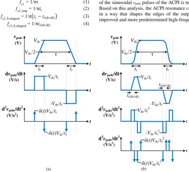
The frequency response of pulse-trains commonly found in power converters is reviewed in this section, as it is the foundational theory for designing the ACPI for high-frequency attenuation purposes. Here, the frequency response of the trapezoidal, the S-shaped, and the sinusoidal pulse-train is briefly discussed. It is assumed that a hard-switched converter has trapezoidal output voltage pulses, and that a soft-switching converter has S-shaped or sinusoidal voltage pulses.
Fig. 3 shows symmetrical trapezoidal and S-shaped pulses of a fixed pulse-width that are successively differentiated, until an impulse train appears [3,35,36]. This graphical representation serves the intuitive interpretation of their high-frequency content: the higher the derivative where the impulse train appears, the lesser the high-frequency harmonic content, and the larger the amplitude of the impulses, the higher that content is [36]. Also featured are the parameters of the pulse-width τ, the rise/fall time tr, and the first-derivative rise time tr(dv/dt) of the
corners of the S-shaped pulse.
The derivative order where the impulse train appears, corresponds to the number of corner frequencies on each symmetrical pulse-train’s spectral envelope. This way, the trapezoidal spectral envelope has two corner frequencies as in (1) and (2): fc1 between the envelope slopes of 0 to -20 dB/dec,
and fc2 between -20 to -40 dB/dec. The S-shaped envelope has
three corner frequencies: while fc1 is the same, the tr(dv/dt)
parameter defines fc2 and a third frequency fc3, as in (3) and (4).
The smooth corners of the S-shaped edges and the introduction of fc3 marks a slope change from -40 to -60 dB/dec. Hence, the
pulse-width τ primarily influences the lower end of the spectrum, and tr and tr(dv/dt) the higher end [3,35,36].
fc1 = 1/πτ (1)
fc2_trap = 1/πtr (2) fc2_S-shaped = 1/π(tr−tr(dv/dt)) (3)
fc3_S-shaped = 1/πtr(dv/dt) (4)
As described in Section II, if only resonant transitions are realised, the output voltage of the ACPI will consist of pulses with sinusoidal edges. If these pulses are assumed as symmetrical and of a fixed pulse-width, the vpole pulse-train will
only have two corner frequencies: the fc1 of (1) and an fc2 that
marks a direct slope change from -20 to -60 dB/dec [37]. However, the successive time-derivative method cannot be applied to sinusoidal edges, as they can be infinitely differentiated, yet they can be approximated as S-shaped, with a small error of about 4 dB, by defining that tr = 2·tr(dv/dt)[36]. The
result is an S-shaped pulse-train where fc2 = fc3. This special
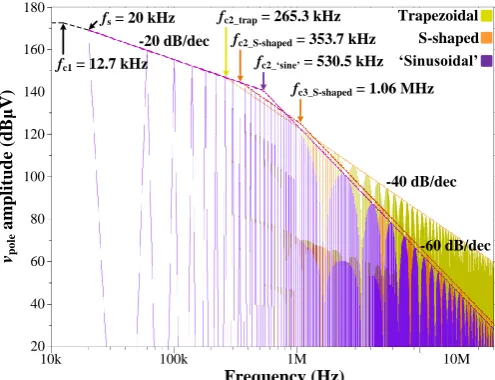
S-shaped pulse maintains the sinusoidal property of the direct slope change to -60 dB/dec. Fig. 4 shows a simulation of trapezoidal, S-shaped, and ‘sinusoidal’ spectra of duty cycle d = 0.5, switching frequency fs = 20 kHz, and symmetrical edges.
It is clearly seen that the -60 dB/dec slope in the S-shaped and sinusoidal spectra results in less high-frequency harmonic content than the trapezoidal spectrum.
In Fig. 4, d is fixed, although the vpole pulse-train of the ACPI
is modulated with Sinusoidal PWM (SPWM), where d varies during T1 and is dictated by the amplitude modulation index mA
[38]. While in this case it is difficult to estimate the harmonic content, it will always be less than the pulse-train of a fixed d = 0.5, i.e., of mA = 0 [39]. As such, the envelope under mA = 0
is always the worst case for the envelope under mA ≠ 0, in the
entire frequency range. If the pulses have identical edges between pulse-trains, the corner frequencies described in (2), (3), and (4) will not be affected.
This analysis highlights that the edges of an S-shaped/sinusoidal pulse can be manipulated in a flexible way, through their duration (tr) and shape (tr(dv/dt)), that is, their smooth
corners. For the reasons discussed above, the frequency response of the sinusoidal vpole pulses of the ACPI is treated as S-shaped.
Based on this analysis, the ACPI resonance can be manipulated in a way that shapes the edges of the output voltage for an improved and more predetermined high-frequency attenuation.
t
r(dv/dt)V
dcV
dc/2
t
τ
t
rt
rt
V
dc/
t
rt
r(dv/dt)t
V
dc/
t
r2-
V
dc/
t
rt
-
V
dc/
t
r 2δ(
t
)
V
dc/
t
r2-δ(
t
)
V
dc/
t
r 2t
rV
dct
v
pole(V)
V
dc/2
t
rτ
t
dv
pole/dt
(V/s)
t
d
2v
pole/dt
2
(V/s2)
V
dc/
t
r-
V
dc/
t
rδ(
t
)
V
dc/
t
r-δ(
t
)
V
dc/
t
rv
pole(V)
dv
pole/dt
(V/s)
d
2v
pole/dt
2(V/s2)
d
3v
pole/dt
3(V/s3)
[image:4.595.108.487.426.771.2](a) (b)
IV. THE EQUIVALENT SERIES LCCIRCUIT
In order to shape the edges of the vpole pulses for an optimum
frequency response, the ACPI resonant process has to be studied. Capacitive turn-offs are not considered in this section, since it is desirable that the vpole edges be sinusoidal only.
A. The Free Oscillation of the Equivalent Circuit and the Quasi-resonant Action of the ACPI
Any resonant transition starts with a set of initial conditions that are dictated by its type (turn-on or turn-off), and by the level and polarity of Iphase. This process is represented as an equivalent
series LC circuit, whose solution is the inductor current iLr and
the output voltage vpole. Figs. 5(a) and (b) illustrate the LC
circuits and their initial conditions for the turn-on and turn-off transitions, when Iphase is positive. These circuits are derived
directly from the circuits in Fig. 2. It is seen that resonance is driven by half the DC-link voltage Vdc/2, while Iphase acts as a
parallel DC load. The 2Cr capacitor between the output node A
and the negative rail represents the two snubber capacitors. The step response of the LC circuits results in iLr and vpole
oscillating sinusoidally with a resonant period Τ0, between a
peak and a valley. The resonant energy available in the circuit depends on the level of Vdc, the properties of Iphase, and the initial
conditions. If the energy increases by raising the iLr(0) initial
condition for example, the sinusoids will oscillate to more extreme peaks and valleys but with the same angular frequency ω0. This is presented in Fig. 5(c), where two vpole waveforms
oscillate freely in response to the energy present in the circuit. Waveform 1 oscillates to more extreme values than waveform 2, due to more energy in the circuit, while ω0 is maintained.
It is important to note however, that the ACPI is a quasi-resonant topology. Resonance only happens when a main switch turns on or off. This contrasts with how other resonant DC-link inverters operate, where the ZVS transitions are realized by a continuously-resonating DC-link voltage. The basic resonant DC-link inverter [15,40] and its derivatives [41] operate in this manner. In the case of the ACPI however, only part of the free oscillation is experienced in the resonant circuit, as vpole swings
between the two DC rail values of (ideally) 0 and Vdc, during the
resonant interval tres. The two DC rail values are not necessarily
at the extremes of the free oscillation, however. As seen in Fig. 5(c), the two vpole waveforms oscillate between 0 and Vdc,
only during the tres intervals. Waveform 1 has a larger amplitude,
meaning that its free oscillation reaches more extreme peaks and valleys than waveform 2. Hence, the tres interval of waveform 1
is shorter, and the dv/dt gradient is larger. The reason for this behaviour is that the amount of energy present in the resonant circuit for waveform 1 is larger than for waveform 2. Consequently, the energy in the resonant circuit dictates the duration (tres) and the shape of the vpole edge between the DC rail
values, impacting the high-frequency response.
B. Boost and Trip Currents
The main difference between the turn-on and the turn-off transitions is the role of Iphase. During the turn-on transition of
Fig. 5(a), iLr flows into A to charge the capacitor, while Iphase
flows out of it as to discharge it, thus inhibiting resonance. When the iLr(0) condition is kept constant, less energy is available to
complete resonance, as Iphase increases during the fundamental
cycle T1. Conversely, in Fig. 5(b), both iLr and Iphase flow out of
A and discharge the capacitor together. If iLr(0) is kept constant,
more energy is put into the circuit as Iphase increases. Under these
conditions, the vpole edge swings faster between the DC rails and
becomes steeper during the turn-off transitions. The opposite trend applies for turn-ons.
A distinction concerning the initial conditions of the currents is necessary at this point. Iboost and Ioff,the currents denoted as
the initial conditions iCr(0) of the capacitor current in Figs. 5(a)
and (b), are the values reached by the outgoing switch current right before resonance starts, as seen in Figs 2(a) and (b). Iboost
and Ioff are termed here as the boost currents and are controlled
by the ramp time intervals tramp. The iLr(0) conditions of a given
turn-on or turn-off transition are also controlled by tramp. In Figs.
2(a) and (b), iLr ramps up to the values of Itrip and Iboca, which are
termed here as the trip currents. Lastly, the relationship between the boost and the trip currents involves Iphase, as seen in Fig. 5.
The trip currents must be large enough to overcome the power loss incurred by the parasitic resistance of the auxiliary circuit [30,42]. The voltage that drives the ACPI resonance is always Vdc/2, and it does not provide enough energy to the
vpo
le
a
m
p
li
tu
d
e
(d
B
μ
V
)
80 100 120 140 160
60 180
40
20
10k 100k 1M 10M
Frequency (Hz)
fs = 20 kHz
-20 dB/dec
-40 dB/dec
-60 dB/dec fc2_trap = 265.3 kHz
fc3_S-shaped = 1.06 MHz
fc1 = 12.7 kHz
fc2_S-shaped = 353.7 kHz
fc2_‘sine’ = 530.5 kHz ‘Sinusoidal’ Trapezoidal S-shaped
Fig. 4. Trapezoidal, S-shaped, and ‘sinusoidal’ spectra with Vdc = 450 V,
fs = 20 kHz, τ = 25 μs, d = 0.5, tr = 1.2 μs, tr(dv/dt) = 300 ns for the S-shaped edges,
and tr(dv/dt) = 600 ns for the ‘sinusoidal’ edges.
+
-
V
dc/2
2
C
ri
LrI
phasev
pole+
-L
rvpole(0) = 0
iLr(0) = Itrip iCr(0) = Iboost
A
(a)
+
-
2
C
ri
Lrv
pole+
-L
rvpole(0) = Vdc
iLr(0) = -Iboca iCr(0) = -Ioff
A
(b)
V
dc0
t
res1t
res2T
0/2
(c)
t
V
dc/2
I
phasev
pole [image:5.595.42.290.58.248.2]2
1
Fig. 5. Equivalent series LC circuit of (a) a switch turn-on transition, (b) a switch turn-off transition when Iphase > 0, and (c) ACPI quasi-resonant action applied to
[image:5.595.40.557.652.761.2]resonant circuit for overcoming that power loss. Thus, additional inductor current is required for compensating the loss, and allowing vpole to swing fully to the opposite rail and achieve
ZVS. Conversely, the coupled-inductor inverters [26-29] raise the driving voltage to more than Vdc/2, allowing iLr to reach lower
trip values. Customarily, Itrip = Iphase is set for turn-ons, meaning
that Iboost = 0. This reduces the auxiliary circuit loss. However,
these inverters suffer from high component counts and design complexity. While the boost currentsin the ACPI increase the auxiliary circuit loss and the main device current stress, they allow flexibility in controlling resonance and the duration of the resonant intervals tres. This is crucial, since the tres intervals are
the actual rise and fall times of vpole. As such, this work
investigates the ACPI for high-frequency content attenuation. Also, interesting trade-offs arise between the power efficiency and the output voltage high-frequency attenuation, due to the existence of the boost currents and the way they are controlled.
C. Analytical Expressions of the Equivalent Circuits
The equivalent circuits are described by ordinary differential equations that yield sinusoidal iLr and vpole
expressions, as in (5) and (6) for turn-ons, and (7) and (8) for turn-offs. A positive Iphase and no auxiliary circuit loss are
assumed. Also during resonance, iLr is bounded by its trip values
Itrip and Iboca, and vpole swings between 0 and Vdc, like in Fig. 2.
iLr = Iphase+Iboostcos(ω0t) + Vdc /2
Z0 sin(ω0t) (5)
vpole = V2dc[1−cos(ω0t)] +Z0Iboostsin(ω0t) (6) iLr = Iphase−Ioffcos(ω0t) −Vdc
/2
Z0 sin(ω0t) (7)
vpole = V2dc[1+cos(ω0t)] −Z0Ioffsin(ω0t) (8) Z0 and ω0 are the resonant impedance and the resonant
frequency, respectively, and depend on the values of the resonant components Lr and Cr, as in (9) and (10). Z0 and ω0 are
valid for both equivalent LC circuits.
Z0 = √Lr/2Cr (9) ω0=1/√2LrCr (10) Solving (5) for iLr = Itrip and (7) for iLr = |Iboca|, yields the
expression for tres_on in (11), and for tres_off in (12).
tres_on =ω2 0tan
-1[ Vdc/2
Z0(Itrip−Iphase)]= 2 ω0tan
-1( Vdc/2
Z0Iboost) (11)
tres_off =ω2
0tan
-1[ Vdc/2
Z0(|Iboca|+Iphase)]= 2 ω0tan
-1(Vdc/2
Z0Ioff) (12)
It is notable that the boost currents Iboost and Ioff appear in (5),
(6), (7), (8), (11) and (12). Hence, for given circuit conditions Vdc and Iphase, and for given Lr and Cr values, the boost currents
affect the resonant magnitudes and the resonant intervals. By properly controlling the boost currents, vpole can be profiled with
slow and smooth edges for reduced high-frequency content, in a predetermined way, and in line with the theory of Section III.
V. FIXED-TIMING AND VARIABLE-TIMING CONTROL
The thorough analysis of the equivalent LC circuit serves for deriving the ACPI control schemes. The two classic ACPI schemes are fixed-timing and variable-timing control [33]. In [43,44] these terms refer to the inductor current ramp interval
tramp. If these intervals are fixed throughout the fundamental
cycle T1, fixed-timing control is realised. If they vary,
variable-timing control is realised. This terminology has also been applied to the conduction period taux_sw of the auxiliary devices
[33]. Regardless of the parameter they refer to, these schemes differ in ease of implementation, current stress, power loss, and most importantly, in high-frequency harmonic attenuation.
Fixed timing is simple to implement. The tramp intervals
described by (13) and (14) are fixed and are manually set into the control algorithm. This means that for given Lr and Vdc
values, the trip currents Itrip and Iboca are fixed throughout T1.
tramp_on = LrItrip
Vdc/2 =
Lr(Iboost + Iphase)
Vdc/2 (13)
tramp_off = LrV|Iboca|
dc/2 =
Lr(Ioff − Iphase)
Vdc/2 (14)
Moreover, the control algorithm uses the Iphase polarity
information for selecting the appropriate auxiliary switch that for a given resonant transition: Sa1 helps with turn-ons and Sa4
with turn-offs, when Iphase is positive. When Iphase is negative, the
auxiliary switches swap roles. However, this scheme can be greatly simplified if the tramp intervals are set equal, i.e., tramp_on =
tramp_off. As such, Itrip = Iboca and the control algorithm sees no
distinction between a turn-on and a turn-off transition. This simplification results in no current and voltage sensing for the purpose of resonance.
The simple fixed-timing scheme comes at the expense of increased current stress and power loss [33]. Firstly, the iLr pulse
currents are unnecessarily high, as seen in Fig. 6(a). This means that throughout T1, the current stress in the auxiliary devices is
severe due to the large iLr peaks. Secondly, the RMS value ILr_rms
of iLr is large, causing high auxiliary circuit loss. Thirdly, the
main device current stress increases, especially during the resonant turn-offs when Iphase is near its peak value Iphase_pk.
According to Ioff = Iboca + Iphase, Ioff becomes excessively large
when Iphase_pk is reached, as Iboca is fixed throughout T1. Hence,
the peaks of the main switching currents iS1 and iS4 in Fig. 2(b),
become very large at Iphase_pk. Lastly, due to both the Iboost and Ioff
contributions in iS1 and iS4, the conduction losses of the main
devices are increased.
Variable-timing control reduces current stress and power loss by varying the tramp intervals [33], which builds the trip
currents and the overall iLr pulses according to the Iphase level. As
seen in Fig. 6(b), the turn-on pulses are initially small, then turn larger as more iLr contribution is required at higher Iphase levels.
The reverse trend holds for the turn-off pulses, since, as explained in Section IV, less iLr contribution is required as Iphase
increases. Thus, ILr_rms and the peaks in the main device currents
are reduced. However, this optimized scheme is more complex, because the Vdc value, and the Iphase level and polarity
information are required for the online calculation of the tramp
intervals of (13) and (14).
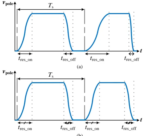
Most importantly, the fixed- and variable-timing schemes have a profound influence on how resonance transpires, which affects the high-frequency signature of vpole. As (13) and (14)
indicate, under fixed timing, the boost currents Iboost and Ioff vary
throughout T1, since the trip currents Itrip and Iboca are fixed. In
turn, the resonant intervals tres_on and tres_off vary during T1,
according to (11) and (12). As explained in Section IV, when the trip currents are fixed, the resonant energy increases for turn-offs and decreases for turn-ons, as Iphase increases. This erratic
terms of edge duration and shape. As a result, the frequency response will not be as predictable as the spectra of Fig. 4.
In contrast, under variable-timing control, the varying tramp
intervals of (13) and (14) mean that they can be controlled in a way that Iboost and Ioff become fixed during T1. In turn, the
resonant intervals will become fixed throughout T1, as dictated
by (11) and (12). This means that the energy put into resonance is more consistent as Iphase varies. The vpole edges will then be
shaped in a consistent manner from one switching cycle to the next, and the frequency response can become more predictable. This is preferable for high-frequency harmonic attenuation. The vpole pulses generated by each scheme are shown in Fig. 7. In
Fig. 7(a) it is seen that fixed timing produces edges that change from one switching cycle to the next, whereas in Fig. 7(b) the edges are consistent in duration and shape under variable timing.
In addition, the variable-timing control algorithm can be set up in such a way that the boost currents are both fixed and equal during the fundamental cycle, i.e., Iboost = Ioff. Then, as dictated
by (11) and (12), the resonant intervals will also be equal, i.e., tres_on = tres_off. The consequence of this condition is the
generation of vpole pulses with the same rising and falling edges.
In other words, the pulses can become symmetrical and the high-frequency response of the output voltage will be similar to the one of a sinusoidal-edge pulse-train, as simulated in Fig. 4.
Conclusively, proper boost current control is essential to the active control of the ACPI resonant magnitudes [45,46], with the overall loss and current stress depending on the properties of the inductor current iLr, and the high-frequency attenuation
capability depending on the edge properties of the output voltage vpole. The two ACPI control schemes that were introduced in this
section influence the way the boost currents inject energy into the resonant circuit during each switching cycle, and therefore have a direct effect on the resonant magnitudes.
VI. DESIGNING THE ACPI FOR HIGH-FREQUENCY CONTENT
ATTENUATION
In this section, the design procedure for the experimental 3-phase ACPI prototype is presented. The timing constraints imposed by the soft-switching action are defined, and the boost current condition for symmetrical vpole pulses is introduced,
along with its advantages and disadvantages. Lastly, capacitive switch turn-offs are also considered.
A. Timing Constraints
Successful soft switching depends on two factors. Firstly, vpole must swing fully to the opposite rail. This achieves ZVS,
and vpole edges that are completely shaped by resonance. If this
does not happen, then an abrupt jump of high dv/dt will be experienced across the large snubber capacitors, and current spikes that are harmful to the main devices might appear.
Secondly, iLr must diminish to zero after a transition has
ended and steady state is reached. If the auxiliary switch is turned off before iLr becomes zero, the slew rate diLr/dt of the
inductor current will sharply increase, causing an overvoltage in the auxiliary branch. The clamping diodes in Fig. 1 will protect the auxiliary devices against this overvoltage, but the control should avoid this scenario, as the voltage spikes and the sharp diLr/dt can be secondary sources of EMI. To avoid this
possibility, the conduction period of the auxiliary devices taux_sw
is the first parameter to be set, and it is common to both the fixed-timing and the variable-fixed-timing schemes. The iLr pulse-width,
denoted as taux, must be fully accommodated by taux_sw during any
transition of T1. As such, the taux_sw interval can be forced to vary
along with taux, but that would involve sensing the actual iLr
pulses, which is a costly and difficult thing to do.
Instead, a fixed taux_sw is selected, a value that lies in the range
of taux_max < taux_sw < dmin·Ts. The lower limit taux_max is the
pulse-width of the tallest and widest iLr pulse that appears during T1.
This specific pulse is built duringthe turn-on transitions at the phase current peaks ±Iphase_pk, and its width is defined as taux_max
= 2tramp + tres_on_max under fixed-timing control, and as taux_max =
2tramp_on_max + tres under variable-timing control. The upper
boundary dmin·Ts is the minimum pulse-width of the SPWM
signal, with dmin the minimum duty cycle and Ts the switching
period, and setting it as the upper boundary ensures that the auxiliary switch is gated off before the next transition begins. This boundary Ts shrinks if the switching frequency fs and/or the
modulation index mA are increased. The modulation-imposed
constraints on soft switching are more stringent since the transition times usually last an order of magnitude longer than with hard switching.
t
t
res_onv
polet
res_offt
res_ont
res_offt
t
res_ont
res_offt
res_ont
res_off(a)
(b)
v
poleT
s
T
sFig. 7. Part of the vpole pulse-train under (a) fixed-timing, and (b)
variable-timing control when Iphase > 0. switch turn-on
Itrip
Iboca
Iphase_pk switch turn-off PWM
t
(a)
t
(b)
Iphase_pk Itrip2
Itrip3 Itrip4
Iboca1
Iboca2
Iboca3
[image:7.595.305.558.521.760.2]Iboca4 Itrip1
Fig. 6. Comparison of iLr pulses with (a) fixed-timing, and (b) variable-timing
[image:7.595.41.282.545.759.2]B. The Boost Current Condition
As discussed in Sections IV and V, the boost currentsdictate the amount of energy provided to the resonant circuit per switching cycle. This in turn affects iLr and vpole, as well as tres_on
and tres_off, according to (5), (6), (7), (8), (11) and (12).
The main focus of the design procedure is the attenuation of the high-frequency content of vpole. Essentially, its frequency
response should be optimized compared to an equivalent hard-switched inverter, by exhibiting a corner frequency fc2 early in
the spectrum and a -60 dB/dec roll-off at high frequencies, as discussed in Section III. Hence, the resonant intervals are demanded to be at least 5 or 10 times longer than hard switching. Theoretically, an optimised vpole frequency response can be
achieved more easily if it is demanded that tres_on = tres_off, as this
will ideally generate a train of symmetrical pulses, and a frequency response that is as predictable as possible. This way, only one tres value will have to be selected. This can only happen
with variable-timing control, which is why it is the first control scheme to be designed. Symmetry in the vpole pulses can
theoretically be achieved by demanding that:
Iboost = Ioff = Iphase_pk (15)
This boost current condition given in (15) means that during the longest turn-on transition at Iphase_pk, the maximum trip
current will be Itrip_max = Iphase_pk + Iboost = 2Iphase_pk. A maximum
value for the ramp interval tramp is then selected that complies
with (15), while respecting the taux_max < taux_sw condition. Hence,
(13) becomes:
Lr= Vdc ∙ tramp_on_max
4 Iphase_pk (16)
With tres selected beforehand, the snubber capacitor Cr can be
designed with the combination of (11), (9) and (10).
Now that the variable-timing scheme is designed, a fixed-timing scheme follows by demanding that the resulting tres_on_max
interval, the longest that will appear, is equal to the tres of the
variable-timing scheme, while Lr and Cr are kept the same.
Additionally, no current or voltage sensing is required, when the trip currents are set equal, that is, Itrip = Iboca. A SABER
simulation of the simplified fixed-timing scheme provides a worst-case scenario for the current stress that will be experienced in the inverter. The maximum Ioff value defines the
repetitive pulsed collector current of the main devices, and the ILr_rms value defines the auxiliary device continuous current.
Finally, the peak of the tallest iLr pulse current defines the pulsed
collector current rating of the auxiliary devices.
At this point, the significance of the boost current condition of (15) needs to be discussed. This discussion only applies to variable-timing control, since it is the only scheme that can result in fixed boost currents. The boost current condition ideally guarantees symmetry in the vpole pulses and an optimised
high-frequency response, but comes at the cost of increased current stress and power loss. Firstly, the iLr pulses during turn-ons will
be too high, since Itrip =
I
boost+ Iphase will increase from Iphase_pkwhen Iphase = 0, to 2·Iphase_pk when Iphase = Iphase_pk. Conventionally,
Iboost must be just large enough to overcome the impact that the
parasitic resistance of the auxiliary circuit has on resonance [43]. In other words,
I
boost provides extra energy to the resonant circuit, so that vpole can swing fully to the opposite DC rail. If theboost current condition is not applied, Iboost can be reduced to a
value that is small enough for successful ZVS, and at the same time for decreased current stress and power loss in the inverter.
The turn-on transition at Iphase_pk results in the tallest and
widest iLr pulse during T1. Its amplitude is described in (17):
ILr_pk_max=Iphase_pk+√(2VZdc
0)
2
+Iboost2 (17) The ILr_pk_max peak currentis an indicator for the current stress
and the power loss experienced in the auxiliary circuit. A larger value of Lr will increase the resonant impedance Z0 and will
reduce ILr_pk_max, but it will lead to a larger and bulkier resonant
inductor [32]. Also, it is not ensured that ILr_rms will decrease,
since for a larger Lr, the tramp intervals will increase according to
(13) and (14), and the iLr pulses will widen. Alternatively, Iboost
can be reduced, though an investigation of (17) shows that ILr_pk_max would not decrease dramatically if Iboost became smaller
than Iphase_pk, not even if Iboost were zero. Hence, undoing the
boost current condition just for reducing the value of Iboost, would
present slight gains in current stress and power loss reduction. The greatest disadvantage of the boost current condition is not that Iboost becomes too large, but the demand that every
turn-off transition must be resonant. This is desirable if every single vpole pulse is to be sinusoidal and symmetrical in a controllable
way. However, the Ioff boost current cannot be smaller than
Iphase_pk, if every off is to be resonant. For example, the
turn-off transition at Iphase_pk can only be resonant if Ioff is at least equal
to Iphase_pk, meaning that Iboca is 0 (since Ioff = Iphase + |Iboca|). If,
however Ioff < Iphase_pk, then |Iboca|< 0, which is impossible. This
way the turn-off transitions around Iphase_pk will not be resonant.
Consequently, the only way to examine any drastic trade-offs between power loss/current stress and high-frequency attenuation is to employ capacitive turn-offs that do not require the participation of the auxiliary circuit. As a final note, setting Iboost = Ioff > Iphase_pk will not bring about any benefits to either the
power loss/current stress, or the high-frequency attenuation. An ACPI design that focuses primarily on achieving a predictable and attenuated high-frequency response for its output voltage will result in increased power loss and current stress, as opposed to a design that focuses on decreasing switching loss. References [42] and [47] discuss how the boost currents can be selected not only for minimised power loss, but also for other important issues such as DC-link utilization, output voltage quality, and mid-point balancing.
C. Capacitive Turn-offs
Fig. 2(c) shows a capacitive switch turn-off, during which vpole transitions in a linear fashion, rather than a sinusoidal one,
since only the snubber capacitors are involved. While the turn-on transititurn-ons are always resturn-onant, resturn-onant turn-off transititurn-ons can be swapped for capacitive ones, but only when Iphase is
sufficiently high. Therefore, a threshold Ith is introduced for
Iphase. Above Ith, the auxiliary circuit is disabled during turn-offs
and only the snubber capacitors are used. The control complexity increases this way [42], but current stress and power loss are alleviated, as several iLr pulses are dropped. However,
the generation of linear vpole edges is not controllable by the
algorithm, but depends on the Iphase level and the value Cr of the
snubber capacitors. As Iphase increases, the duration of the linear
edges tcap_off decreases, as in (18).
tcap_off = 2CrVdc
Iphase (18)
Ith should not be set too low, or else tcap_off will become too
scheme and it cannot be altered. As such, Ith is constrained by
the modulation scheme. The transition at Iphase = Ith will occur at
a specific point in the fundamental cycle. Therefore, the pulse-width of the SPWM signal at that point in T1 must be
considered. During the transitions around Ith, the longest
capacitive turn-off transition of duration tcap_off_max will be
followed by a resonant turn-on transition of duration tres. The
pulse-width of the SPWM signal must be large enough to accommodate both transitions. Otherwise, if tcap_off_max is too
long, the vpole pulse will be deformed or even dropped.
D. Selection of the Design Parameters
In this subsection, the design procedure for the experimental 3-phase ACPI prototype is presented. Firstly, a common SPWM modulation scheme is chosen for both the soft-switching and the hard-soft-switching inverters with a fundamental frequency of f1 = 400 Hz, a switching frequency of fs = 20 kHz,
and a modulation index of mA = 0.83. The 3-phase load is in a
star connection, with Rphase = 10 Ω and Lphase = 2 mH. The above
circuit conditions lead to a peak phase current of Iphase_pk = 18 A,
when the DC-link voltage is Vdc = 500 V.
Since the vpole frequency response is to be optimised with
respect to hard switching, a long enough tres is demanded,
during which the vpole edges are shaped. Additionally, a
symmetrical vpole pulse-train is desired under variable timing.
Under these considerations, the resonant intervals are demanded to be tres_on = tres_off = 1.2 μs. At the same time, the
boost current condition of (15) is applied for a symmetrical vpole
pulse-train. Thus, Iboost = Ioff = Iphase_pk = 18 A is set.
The SPWM scheme imposes a constraint of a minimum pulse-width of dmin·Ts = 4.2 μs. The resultant pulse-width of the
widest and tallest iLr current pulse is demanded to be quite
smaller at taux_max = 2 μs. With tres = 1.2 μs, the maximum ramp
interval that will appear under the variable-timing scheme is tramp_on_max = 400 ns, since taux_max = 2·tramp_on_max + tres. The
taux_max pulse-width can now be accommodated by a fixed
auxiliary switch conduction period of taux_sw = 2.2 μs.
Next, the values of the resonant components are estimated. Since tramp_on_max = 400 ns and the boost current condition is set
as shown above, (16) results in Lr = 2.7 μΗ. Then, since
tres = 1.2 μs and Iboost = 18 A, (11) leads to Cr = 47 nF.
Fixed-timing control is then designed, while maintaining Lr
and Cr, and demanding that the maximum resonant interval that
will appear during T1 is tres_on_max = 1.2 μs. Moreover, the
fixed-timing scheme is simplified by setting the trip currents to a fixed value of Itrip = Iboca = 36 A, which can be achieved with a fixed
tramp = 400 ns. Simulating this scheme in SABER predicts that
the RMS value of iLr is ILr_rms = 15 A, and that during the
turn-on transititurn-on at Iphase_pk, the largest iLr peak is ILr_pk_max = 68 A.
Furthermore, during the turn-off transition at Iphase_pk the largest
boost current for turn-offs is Ioff_max = 54 A. These parameters
are useful for selecting the device current ratings.
Finally, a phase current threshold of Ith = 12 A is introduced
to the variable-timing scheme, above which the auxiliary circuit is disabled and the turn-off transitions are realised only by Iphase
and the snubber capacitors. With Ith = 12 A, the longest
capacitive turn-off that will appear during T1 is
tcap_off_max = 3.9 μs, according to (18).
In summary, a fixed tres value is selected for generating a
symmetrical output voltage pulse-train under variable-timing control, and the boost current condition is set. Then, a global fixed auxiliary switch conduction period taux_sw is set. Next, the
Lr and Cr are calculated. A fixed-timing scheme is then designed
for sizing the main and auxiliary devices. Lastly, capacitive turn-offs are introduced for examining any trade-offs that may arise between the decreased power loss/current stress, and the high-frequency content attenuation.
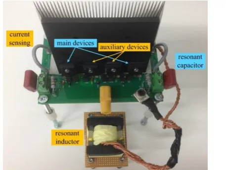
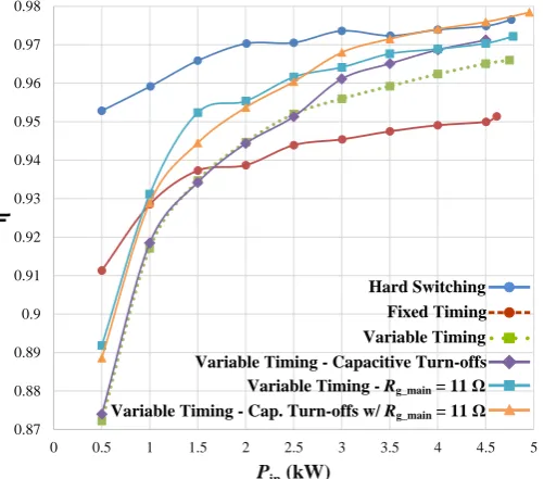
VII.EXPERIMENTAL RESULTS
A 3-phase 5-kW ACPI prototype was built for validating the proposed method of high-frequency harmonic attenuation. Fig. 8 shows a single-phase ACPI module. Three of them connected to a common DC link, form the 3-phase ACPI. Two 1200V/40A IKW40N120T2 IGBT copacks from Infineon constitute the main devices (S1 and S4), and two 600V/35A
NGTB35N60FL2WG IGBT copacks from ON Semiconductor the auxiliary ones (Sa1 and Sa4). The resonant components can
be easily disconnected for hard-switching tests.
A Xilinx XC3S400 FPGA executes the PWM algorithm. Under hard switching it is input with a tdead = 1.2 μs dead-time,
and with a taux_sw = 2.2 μs under soft switching. Variable timing
relies on the online calculation of (13) and (14) by a TI F28335 DSP, which is based on the manually-input boost current condition of Iboost = Ioff = 18 A, and the Vdc and Iphase levels.
These are sensed by AD7667 analog-to-digital converters. The Iphase polarity selects the appropriate auxiliary switch. In
addition, capacitive turn-offs are realised by introducing a threshold of Ith = 12 A to the variable-timing scheme. Fixed
timing requires only the input of tramp = 400 ns that leads to the
condition of Itrip = Iboca = 36 A.
A modified gate driver based on a Schmitt trigger can sense the zero-crossing of the voltage across the main devices [48], for turning on the incoming switch at the end of tres, making for
load-adaptive control. This however will add more complexity. Instead, a fixed 1.2-μs delay is introduced to the PWM algorithm that starts as soon as the outgoing switch is gated off. After the delay, the incoming switch is gated on. Experimental trial and error is required for tuning this delay.
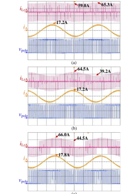
3-phase experiments are presented with a DC-link voltage of Vdc = 450 V, under hard switching, fixed timing, variable
timing, and variable timing with capacitive turn-offs. Only phase A results are presented, due to the 3-phase symmetry.
[image:9.595.326.555.600.772.2]A. Fundamental Cycle and ZVS
Fig. 9 shows the phase A current iA, the output voltage vpole,
and the inductor current of phase A iLrA, for two fundamental
cycles under fixed timing in Fig. 9(a), variable timing in
Fig. 9(b) and variable timing with capacitive turn-offs in Fig. 9(c). In Fig. 9(a), iLrA does not vary much with iA, as the
current pulses are unnecessarily high, whereas in Fig. 9(b) the variation of iLrA with iA is stronger, as the pulse amplitudes get
smaller in certain intervals. This way, the RMS value is ILrA_rms
= 11.2 A under fixed timing, and ILrA_rms = 9.5 A under variable
timing. In Fig. 9(c), the iLrA turn-off pulses (negative pulses for
iA > 0, positive pulses for iA < 0) above the Ith level are dropped.
This way, ILrA_rms is even smaller at 8.9 A. Overall,
variable-timing control can decrease current stress and the auxiliary circuit loss, since the iLrA pulses are built according to the phase
current level. Capacitive turn-offs further reduce current stress and power loss.
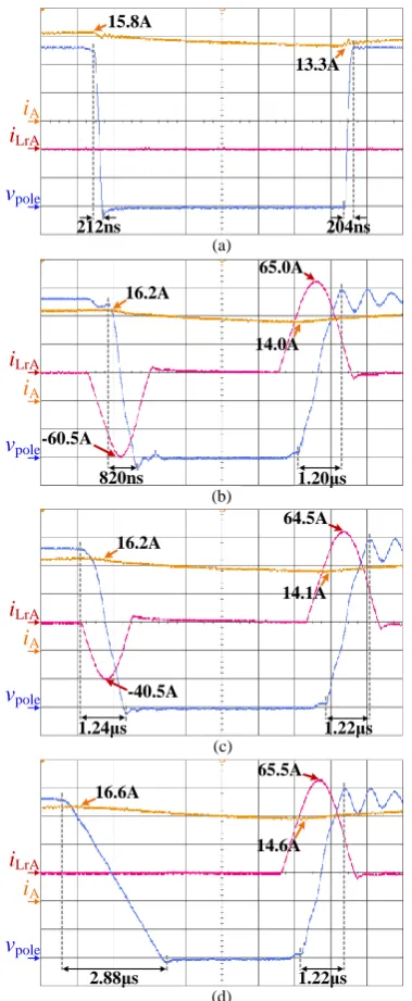
Fig. 10 shows the ZVS transitions of the main switch S1 at peak
phase current IA_pk. Current iS1 and voltage vS1 are shown during
the turn-on and turn-off transitions under hard switching in Figs. 10(a) and (b), and under variable timing in Figs. 10(c) and (d). The capacitive turn-off transition is shown in Fig. 10(e). During the transition of Fig. 10(a), the reverse recovery current of the main diode D4 causes iS1 to peak to double the iA level.
Also, the tail of iS1 in Fig. 10(b) worsens the hard-switching
turn-off loss. In contrast, soft switching decouples the edges and minimize switching loss, as shown in Figs. 10(c), (d) and (e). Variable timing fully decouples the edges in Fig. 10(c). There is a large overshoot in iS1 though, due to the ringing caused by
the parasitic inductance of the switching loop. In Fig. 10(d), iS1
peaks to 29.4 A due to the Ioff component. Also, the edges in
Fig. 10(d) are not decoupled fully due to the tail current bump of 6.6 A that iS1 exhibits. This peculiar bump occurs in IGBTs
only when they turn off under ZVS [49]. Generally, more turn-off loss is incurred in the ACPI than turn-on loss [33], unless capacitive turn-offs are used, as in Fig. 10(e), in which case the ACPI operates as an almost lossless turn-off snubber. Overall, soft-switching decouples the transitioning edges and achieves ZVS, especially under resonant ons and capacitive turn-offs, whereas hard switching does not, with the penalty of increased switching loss.
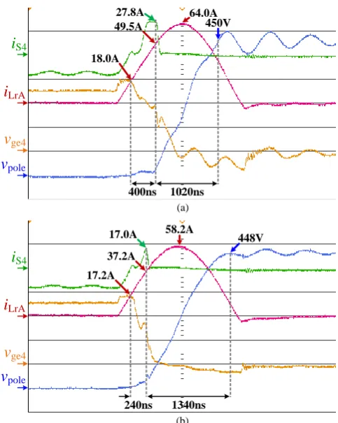
B. Resonant Transitions & Output Voltage Edge Generation Of major importance in this work is how the four switching modes generate the output voltage edges. This comparison is
vpole
iA
iLrA
17.2A
65.3A 59.0A
17.2A 64.5A
39.2A
17.8A 66.0A
44.5A (b) (a)
(c)
vpole
iA
iLrA
vpole
iA
iLrA
Fig. 9. Phase A current iA, output voltage vpole, and phase A inductor current iLrA
under (a) fixed timing, (b) variable timing, and (c) variable timing with capacitive turn-offs over two fundamental cycles. iA 20A/div, vpole 250V/div,
iLrA 50A/div, time 0.5ms/div.
vS1
iS1
28.9A
14.4A 453V
454V
37.5A
16.2A
29.4A 16.2A
452V 486V
6.6A
17.2A 4.4A
454V 479V 20V (a)
(c)
(e) (d) vS1
iS1
vS1
iS1
vS1
iS1 15.9A
525V 453V
13.9A
(b) vS1
iS1
Fig. 10. Switching current iS1 and voltage vS1 during the transitions of S1 at peak
phase current IA_pk. (a) Hard-switched turn-on and (b) turn-off, (c)
variable-timing turn-on and (d) turn-off, and (e) variable variable-timing with capacitive turn-off. Hard switching: vS1 80V/div, iS1 10A/div, time 200ns/div. Soft switching: vS1
[image:10.595.313.521.183.737.2] [image:10.595.41.256.402.743.2]