City, University of London Institutional Repository
Citation
:
Dhingra, N., Song, J., Ghosh, S. ORCID: 0000-0002-1992-2289, Zhou, L. and
Rahman, B. M. A. ORCID: 0000-0001-6384-0961 (2018). Design of phase change
Ge2Sb2Te5 based on-off electro-optic switch. Proceedings of SPIE, 10537, 105370Z.. doi:
10.1117/12.2287218
This is the accepted version of the paper.
This version of the publication may differ from the final published
version.
Permanent repository link:
http://openaccess.city.ac.uk/20694/
Link to published version
:
http://dx.doi.org/10.1117/12.2287218
Copyright and reuse:
City Research Online aims to make research
outputs of City, University of London available to a wider audience.
Copyright and Moral Rights remain with the author(s) and/or copyright
holders. URLs from City Research Online may be freely distributed and
linked to.
City Research Online:
http://openaccess.city.ac.uk/
[email protected]
Design of Phase Change Ge
2Sb
2Te
5based ON-OFF Electro-Optic
Switch
Nikhil Dhingra
1, Junchao Song
2, Souvik Ghosh
2, Linjie Zhou
3and B. M. A. Rahman
21
Department of Electronic Science, University of Delhi South Campus, Benito Juarez Road, New
Delhi – 110021, India
2
Department of Electrical and Electronic Engineering, City, University of London, London, EC1V
0HB, U.K.
3
State Key Laboratory of Advanced Optical Communication Systems and Networks, Department of
Electronic Engineering, Shanghai JiaoTong University, Shanghai 200240, P. R. China
ABSTRACT
Design of electro-optic ON-OFF switches based on well-known phase change material Ge2Sb2Te5 (GST) is presented. The electro-optic switch is achieved by implementing by co-directional coupling between a 220 nm thick silicon nanowire and a silicon waveguide topped with ITO-GST-ITO layers at the 1.55μm wavelength. By introducing the electric field via the ITO electrodes, the GST layer can be changed between the amorphous and crystalline states. As the modal loss in the crystalline state is much higher than the amorphous state, through a rigorous modal analysis of the coupled silicon nanowire and GST waveguide by using the finite element method, the optimal ITO spacing is obtained at 75nm which is less sensitive to device parameter variations and thus offering better tolerances. The GST thickness is also optimized for the phase matching point at 25 nm in order to efficiently transfer power from silicon nanowire to GST waveguide to attain the OFF state. Once the device is phase matched in crystalline state, the power in the amorphous state will pass with very little interaction with the GST waveguide resulting in an ON state. The Eigenmode Expansion Method of Fimmprop is used as a junction analysis approach to calculate the optical power coupling efficiencies to the output silicon nanowire. The extinction ratio of the electro-optic switch and insertion loss in ON state at phase matching can be obtained as a function of the device length. A compact 1.75 μm long device shows a high extinction ratio of 22 dB with an insertion loss of only 0.56 dB.
Keywords: electro-optics; switching; phase change material; GST.
1.
INTRODUCTION
The small size active and passive photonic devices are the key components to achieve large scale photonic integrated circuits (PICs). Devices based on silicon-on-insulator platform are very promising due to reduced chip footprint and power consumption and their compatibility with microelectronic circuits based on CMOS technology. Normally, there are two approaches to design Si-based modulating and switching devices, and there are carrier injection and carrier depletion. For carrier injection modulators, carriers are injected by forward biasing the junction. This type of the modulator is limited in speed by the recombination rate of the carriers, and relatively high power consumption. But it has the advantage of that it can allow large changes in the carrier density and therefore a high modulation depth. On the other hand, carrier depletion, which modulate carrier density by reverse biasing junction, it is fast and consumes lower power as little current flows through the junction. But because of its need to have higher overlap the PN junction and the optical field, it leads to devices have large insertion loss and low modulation depth. Moreover, the Si-based modulator with carrier injection require control region length often longer than 100 µm. On the other hand, although resonant structures such as ring resonator may require a smaller length but provides only a narrow operation bandwidth but with a strong wavelength dependence.
to mitigate some of these problems encountered by carrier based modulators. For example, vanadium dioxide (VO2) is a correlated electron material that has an insulator-metal phase transition at 68 ℃. Although VO2 undergoes a large refractive index change during its phase transition, the loss in insulator and metal phases is also large and these need to be evaluated for their useful applications. Several electro-optic devices based on the phase change material Ge2Sb2Te5, commonly known as GST, have been reported have better optical performance than the VO2 [1], [2]. These devices utilize high differential refractive index between the amorphous and crystalline states to provide compact electro-optic devices. The phase change of the GST can be achieved thermally [3], optically [4], or electrically induced potentially with an ultrahigh speed [5]. In addition to that, unlike other electro-optic materials, GST possesses the self-holding feature, which means it requires energy only to switch from one state to another, but no continuous supply of energy is needed to maintain in a given state.
In this paper, we consider a novel co-directional coupling between the GST waveguide and the silicon nanowire for designing a compact electro-optic ON-OFF switch at the telecommunication wavelength, 1.55 µm.
2.
DEVICE DESIGN
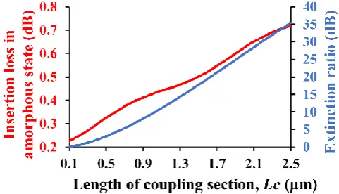
Figure 1(a) shows the three-dimensional view of the optical switch. The cross-sectional view of the coupled section is shown in Fig. 1(b). The coupled section consists of a silicon Nanowire (wg1) and an ITO-GST-ITO-air waveguide (wg2). The required electric field for changing states between crystalline and amorphous can be provided through the two ITO electrodes. Here, most commonly used 220 nm thick silicon core is considered, and its width is taken as 550 nm. On top of that an ITO layer with thickness, SITO is taken as the separation layers to control the coupling. On top of the ITO separating layer is a GST layer with thickness hGST is fabricated and its thickness can be controlled to achieve the phase matching. On top of the GST layer is another ITO layer, the thickness hITO is taken to facilitate the application of electric field. The refractive indices of Si, SiO2 and ITO are taken as 3.47548, 1.44402 and 1.9595+j0.0023, respectively at the operating wavelength of 1.55 μm. For GST, the complex refractive indices, 7.45+j1.49 and 4.6+j0.12 are used for its crystalline and amorphous states, respectively [2].
Fig. 1. (a) Schematic of the optical switch. (b) Cross-sectional view of the coupled section of the optical switch.
[image:3.595.143.453.409.532.2]difference ∆α = 4.343(4π*∆neff/ λ), calculated as 7.91 dB/μm. This modal loss in the waveguide will cause incomplete mode cancellation and thus a poor MZI switching. Hence, here we consider an alternative and innovative co-directional coupling design between the GST waveguide and the silicon nanowire for the switch.
[image:4.595.172.423.196.339.2]As the loss for the crystalline state is much higher than the amorphous state, the phase matching in this state is necessary in order to efficiently transfer power from silicon nanowire to GST waveguide to attain the OFF state. If the device is not phase matched in its amorphous state, then the power will guide through the silicon nanowire with very little interaction with the GST waveguide on the top resulting in an ON state. Hence, design objective here is to achieve phase matching the GST waveguide in the crystalline state with the silicon nanowire.
Fig. 2. Real part of effective indices of the even and odd supermodes of the coupled section in crystalline state for two different SITO.
First, the effective index (neff) of the fundamental quasi-TE (Hy11) mode of the wg1 is calculated as 2.4472 and then the thickness of GST (hGST) is varied in wg2 in order to identify the value of hGST for achieving phase matching for a weak coupling. Around this value of hGST, we calculated the neff of the supermodes of the composite coupled structure for two ITO spacing (SITO) of 75 nm and 150 nm. The real parts of neff of the two supermodes as a function of hGST is shown in Fig. 2 for two different separations, SITO.
From the figure, when the SITO is selected at 150 nm, it shows that the Re(neff) of the even supermode shown by an orange line, keeps stable around 2.4 when the hGST increases from 23 nm to 24.5 nm, and after that it continuously increase to a high value 2.7. On the other hand, the Re(neff) of the odd supermode shown by a purple line, initially increase slightly from 2.25 to a stable level around 2.4 when the hGST increases from 23 nm to 24.5 nm then remains constant. It can be noted that the difference between the effective indices (real part) of the two supermodes is minimum at hGST=24.5 nm.
For the SITO=75 nm, the Re(neff) of the even supermode shown by a light green line remains constant around 2.55 when the hGST increase to 25.6 nm, after that it increase smoothly to a higher value 2.7. Meanwhile, the Re(neff) of the odd supermode, shown by a dark green line climbs gradually from 1.9 to 2.1 when the hGST increase from 23 to 28 nm. It also can be observed that, there is a minimum separation point at hGST=25.6 nm, when the Re(neff) lines of even and odd supermode have smallest difference. It can be evaluated that smaller SITO can provided larger Re(neff) difference between the even and odd supermodes, also appears at the bigger hGST for the minimum separation point.
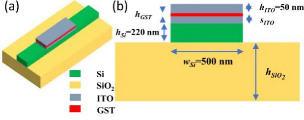
Fig. 3. Coupling length of the coupled section as a function of hGST.
Next, we plotted the mode loss (dB/µm) in the crystalline state as a function of hGST in Fig. 4. For the even supermode, it shows that when the hGST increase from 23 to 28 cm, the modal loss also increase rapidly from 12.5dB/μm to 27.7dB/μm. Because of the power confinement in the GST layer of the waveguide in the even supermode increases from 8.35% to 19.71%, which also leads to a larger absorption loss of the waveguide. On the other hand, the modal loss of the odd supermode will decrease from a higher value of 20.2 dB/μm as the GST layer thickness is increased. It also can be explained by noting that the power confinement in the GST layer is reduced from 10.2% to 5.86%, which leads to the absorption loss the waveguide decrease to a lower value at 10.1dB/μm. It can be noted that around hGST=24.8nm, both the even and odd supermodes will have the similar modal loss values which are 17.5dB/μm.
Fig. 4. Loss values of the supermodes in the crystalline state as a function of hGST for SITO=75 nm.
The phase matching exists at hGST=25.6 nm in crystalline state for SITO=75 nm. For these parameters, the corresponding Hy field profiles of the Hy11 even and odd supermodes are shown in Fig. 5. It can be overserved that in the left figure, the Hy
11
even supermode field profile in the GST waveguide and Si nanowire, both have the same sign. On the other hand, the Hy11 odd supermode field profile in the GST waveguide and Si nanowire have opposite signs. Next, the Hy component of the Hy11 even and odd supermodes along the vertical directions are plotted in Fig. 6. It can be noted that, the Hy11 even supermode have much larger field intensity in the GST waveguide than in the Si nanowire, also the maximum value can be achieved at the interface between the GST and top ITO layers. For the Hy
11
[image:5.595.196.418.389.536.2]Fig. 5. Hy field profiles of the Hy11 even and odd supermodes in crystalline state for SITO=75 nm and hGST=25.6 nm.
Fig. 6. Hy component of the Hy11 even and odd supermodes in crystalline state along the vertical directions (μm).
Around hGST=25.6 nm, which is the value of GST thickness for which both wg1 and wg2 are phase matched in crystalline state, however, its amorphous state supports only one mode. Hence, changing hGST from 23 to 28 nm, in amorphous state, resulted in only a slight variation in the real (neff), from 2.494 to 2.509, and mode loss values, increased from 0.17 to 0.22 dB/µm, which is very low in this case.
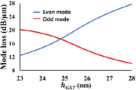
Fig. 7. Power excitation coefficient in crystalline state as a function of hGST for SITO=75 nm.
[image:6.595.184.412.492.629.2]interfaces are shown in Fig.7. When the hGST is 23 nm, it can be seen that the even supermode have a relatively higher transmission at 70%, but the odd supermode only can obtain the 30% transmission coefficient. With the increase of the hGST, this coefficient of the even supermode will reduce considerably to a lower value 35%. While the transmission coefficient of the odd supermode will increase to higher value 65% at this two waveguides junction when the thicker GST layer will be selected at 28 nm.
[image:7.595.177.418.195.333.2]At hGST=25.6 nm, which is the phase matching thickness of GST layer, the excitation coefficients curves cross each other. It can be seen that both even and odd supermodes will have similar excitation coefficients which is close to 50% each, when hGST is euqal to 25.6 nm, as the two waveguides are phase matched in its crystalline state.
Fig. 8. Insertion loss in ON state and extinction coefficient of the device.
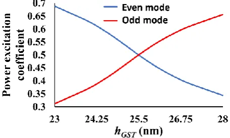
The associated insertion loss for the ON state and the extinction coefficient of the device are plotted in Fig. 8. By calculating the transmission coefficient Tam after the coupled section at the output silicon nanowire, the Insertion loss in the amorphous state for the ON state can be obtained. It shows that with the longer length of the coupling section, the insertions loss also increase from 0.24 to 0.7 dB but still at a relatively lower level.
The extinction ratio ER is defined as the ratio of the two optical power levels when the device in the ON or OFF states. Through numerical simulations of the transmission coefficient, both in amorphous and crystalline state at the output silicon nanowire, the ER can be calculated. From the Fig. 7, it can be seen that when the length of coupling section increase from 0.1 to 2.5 μm, the extinction ratio also increase monotonically to a higher level to 35 dB.
3.
CONCLUSION
We have carried out rigorous modal analyses of an electro-optic switch based on coupling between the silicon nanowire with top ITO layer and the phase change material GST waveguide by using the FEM. We have also investigated the power coupling efficiencies to the output silicon nanowire by using a junction analysis approach. We obtained extinction ratio of the device and insertion loss in ON state at phase matching as a function of length of the device. For a device length of 1.75 µm, a high extinction ratio equals to 22 dB and an insertion loss of only 0.56 dB was achieved.
REFRERENCE
[1] Tanaka, D., Shoji, Y., Kuwahara, M., Wang, X., Kintaka, K., Kawashima, H., Toyosaki, T., Ikuma, Y. and Tsuda, H., “Ultra-small, self-holding, optical gate switch using Ge2Sb2Te5 with a multi-mode Si waveguide,” Opt. Express. 20(9), 10283-10294 (2012).
channel-waveguide electro-optical 2 x 2 switches and 1 x 1 modulators using a Ge2Sb2Te5 self-holding layer,” J. Lightw. Technol. 33(9), 1805-1813 (2015).
[3] Stegmaier, M., R os, C., Bhaskaran, H., Pernice, W., “Thermo-optical Effect in Phase-Change Nanophotonics”, ACS Photonics. 3, 828-835 (2016).
[4] Moriyama, T., Kawashima, H., Kuwahara, H., Wang, X., Asakura. H., Tsuda, H., “Small-sized Mach-Zehnder interferometer optical switch using thin film Ge2Sb2Te5 phase-change material” Optical Fiber Communications Conference and Exhibition, (2014)
[5] Kato, K., Kuwahara, M., Kawashima, H., Tsuruoka, T., Tsuda, T., “Current-driven phase-change optical gate switch using indium–tin-oxide heater,” Applied Physics Express. 10, 072201 (2017).
[6] Liang, H., Soref, R., Mu, J., Huang WP. “Electro-optical phase-change 2 × 2 switching using three- and four- waveguide directional couplers,” Applied Optics. 54(19), 5897-5902 (2015).