Inverse-designed diamond photonics
Constantin Dory
1, Dries Vercruysse
1,4, Ki Youl Yang
1,4, Neil V. Sapra
1, Alison E. Rugar
1, Shuo Sun
1,
Daniil M. Lukin
1, Alexander Y. Piggott
1, Jingyuan L. Zhang
1, Marina Radulaski
1,2, Konstantinos G. Lagoudakis
1,3,
Logan Su
1& Jelena Vu
č
kovi
ć
1Diamond hosts optically active color centers with great promise in quantum computation, networking, and sensing. Realization of such applications is contingent upon the integration of color centers into photonic circuits. However, current diamond quantum optics experiments are restricted to single devices and few quantum emitters because fabrication constraints limit device functionalities, thus precluding color center integrated photonic circuits. In this work, we utilize inverse design methods to overcome constraints of cutting-edge diamond nanofabrication methods and fabricate compact and robust diamond devices with unique specifications. Our design method leverages advanced optimization techniques to search the full parameter space for fabricable device designs. We experimentally demonstrate inverse-designed photonic free-space interfaces as well as their scalable integration with two vastly different devices: classical photonic crystal cavities and inverse-designed waveguide-splitters. The multi-device integration capability and performance of our inverse-designed diamond platform represents a critical advancement toward integrated diamond quantum optical circuits.
https://doi.org/10.1038/s41467-019-11343-1 OPEN
1E. L. Ginzton Laboratory, Stanford University, Stanford, CA 94305, USA.2Present address: Electrical and Computer Engineering, University of California, Davis, CA 95616, USA.3Present address: Department of Physics, University of Strathclyde, Glasgow G4 0NG, UK.4These authors contributed equally: Dries Vercruysse, Ki Youl Yang. Correspondence and requests for materials should be addressed to C.D. (email:[email protected]) or to J.V. (email:[email protected])
123456789
D
iamond has excellent material properties for quantum optics1,2, optomechanics3,4, and nonlinear optics5. Of particular interest is the variety of color centers that diamond hosts, some of which exhibit very long coherencetimes1,6. The development of diamond photonic circuits7
has emerged as a promising route for implementing optical
quantum networks8–18, quantum computers19–21, and quantum
sensors22,23. However, a major challenge in diamond quantum
photonics is the lack of high-quality thinfilms of diamond, as the production of electronic grade diamond can be achieved only in homoepitaxy, and thinning processes are not repeatable enough for photonic crystal cavity fabrication24. As a result,
state-of-the-art diamond cavity quantum photonics relies on angled-etching of bulk diamond24. This technique naturally leads to triangular cross-sections with strongly constrained geometries, which limit device design and functionality. Recent developments in diamond
processing based on quasi-isotropic etching25–28 (see
Supple-mentary Note 1 and SuppleSupple-mentary Figs. 1 and 2) allow the production of diamond membranes with rectangular cross-sections and variable dimensions from bulk diamond. Although rectangular cross-sections are a major step toward diamond integrated circuits, this fabrication technique comes with its own geometric constraints, such as limitations on the range of fab-ricable feature sizes, which originate from a strong correlation of the initial etch depth and undercut thin-film area. Traditional photonic designs that do not account for fabrication constraints are thus unable to take full advantage of this new fabrication technique.
In this work, we overcome these fabrication and design challenges by employing inverse design methods. In silicon nanophotonics these methods have recently attracted consider-able attention for their efficient design of devices with superior
performance over conventional designs29. This optimization
technique searches through the full parameter space of fabricable devices, thereby arriving at solutions previously inaccessible to
traditional design techniques30. We showcase the potential of
inverse design techniques for diamond integrated circuits by designing and fabricating several devices: a compact vertical
coupler, an essential component for large-scale quantum photo-nic systems, and a small circuit consisting of inverse-designed vertical couplers and waveguide-splitters acting as interfaces for two nanoresonators. Our inverse-designed vertical coupler adheres to the diamond fabrication constraints and outperforms commonly used free-space interfaces. The fabricated devices show excellent agreement with simulations in terms of both performance and yield. In the second example, we illustrate the integration of such a vertical coupler into a diamond photonic circuit consisting of two nanobeam resonators connected via inverse-designed waveguide-splitters—a configuration that could be used to entangle two quantum emitters embedded inside such resonators.
Results
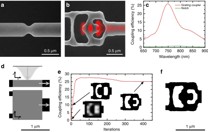
Inverse design of diamond nanophotonic devices. In photonics, grating couplers are frequently used as optical free-space inter-faces31–36. To achieve high coupling efficiencies, such designs typically use asymmetry along the z-axis, e.g., through partial etches31,32,36or material stacks with varying refractive indices32.
In diamond quantum photonics many of these approaches
can-not be employed because current thin-film diamond on silica
substrate platforms33–35do not support state-of-the-art quantum optics experiments20,21,24. Similar approaches with hybrid struc-tures, such as gallium phosphide (GaP) membranes on diamond, offer a platform for efficient grating couplers37. However, the
opticalfield is confined in the GaP membrane and consequently
emitters in diamond couple only evanescently to thefield. A practical solution to these fabrication and design challenges
are notches (Fig. 1a), which are a perturbation to a waveguide
with ≈1% scattering efficiency20. In our work, we develop an
inverse-designed vertical coupler (Fig. 1b) and use the notch
for a baseline comparison. The couplers have a footprint of
1.0 × 1.0μm2 and couple directly to a 400 nm wide waveguide
without a tapering section, assuring compactness. As shown in Fig.1c, the simulated peak efficiencies of the coupler (red) and the notch (green) are ≈25% and ≈1%20, respectively. Further-more, we optimize the vertical coupler to couple the light between
1 μm 1 μm
x z
x y
0.5 μm
0.5 μm 0650 700 750 800 850 900
5 10 15 20 25
0 100 200 300 400
0 5 10 15 20 25 30
Coupling efficiency (%)
Wavelength (nm)
Grating coupler Notch
f e
d
c
b a
Coupling efficiency (%)
Iterations
[image:2.595.116.480.461.692.2]the fundamental free-space mode TEM00and the TE fundamental
mode of the waveguide. Even for conventional grating couplers in
mature photonics platforms the selective coupling to the TEM00
mode is a formidable challenge31,32. The theoretical maximum
coupling efficiency of our couplers is 50%, because of the
symmetry along the z-axis of our devices (i.e., the structure will couple light in+/−z-direction equally).
Inverse design problems in photonics are defined by an
electromagnetic simulation, a design region and afigure of merit to optimize. The starting conditions of the simulation for
vertical couplers are shown in Fig. 1d. A vertically incident
Gaussian beam forms the radiative source and is centered above the 1.0 × 1.0μm2design region shown in gray. To the left of the
design region are two black support bars to suspend the design, and to the right is a black output waveguide. The fraction of incident light coupled into the fundamental TE mode of the
waveguide serves as thefigure of merit and is maximized during
our optimization process (detailed in ref.38). The coupling
efficiency during the optimization is shown in Fig.1e. At the start of the optimization, any permittivity value between that of air and diamond is allowed, which results in a continuous structure shown in the leftmost inset. After several iterations, this structure is discretized, in which case the permittivity is that of either air or diamond. This discrete structure is further optimized while also gradually imposing a penalty on infabricable features39,40. As a
result, the coupling efficiency at a wavelength of 737 nm (silicon-vacancy color center zero-phonon line) peaks at a value of
≈27.5%, which then decreases to≈25% to comply with fabrication constraints40.
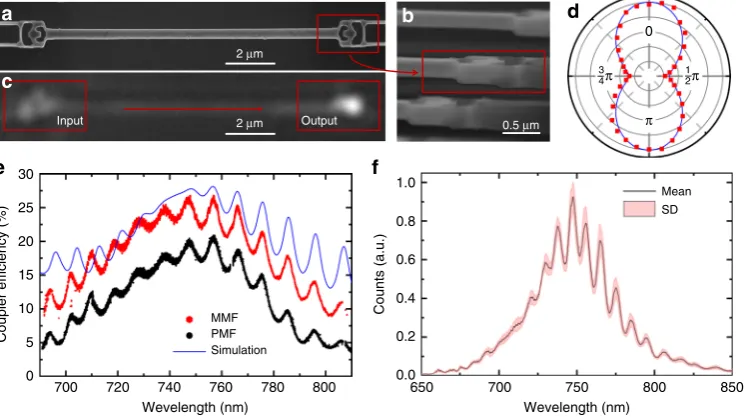
Characterization of diamond vertical couplers. To characterize
the coupling efficiency of the vertical couplers, we measure
the device shown in Fig. 2a, b, in top-down and sideview,
respectively. An optical microscope image of the same structure, presented in Fig.2c, qualitatively shows the high performance of
the vertical couplers. We characterize the polarization depen-dence of the vertical couplers by sweeping the polarization of the
input laser beam (Fig. 2d). The observed fivefold reduction in
the transmitted power when rotating the polarization by π2
corresponds well to our simulated results (blue line in Fig. 2d) and is experimental evidence for excellent coupling to a linearly
polarized TEM00 mode. In Fig. 2e, we present experimentally
determined efficiencies of the vertical couplers, which we acquire by coupling a tunable continuous-wave Ti:Sapphire laser to the structures in a cryostat using a 0.9 NA objective. We then collect the out-coupled beam with a single-mode polarization-maintainingfiber (PMF, black data points) and a multimodefiber (MMF, red data points). The experimental results show peak
efficiencies of ≈21% for PMF and ≈26.5% for MMF, with
broadband performance of >70 nm (PMF) and >90 nm (MMF). The small discrepancy between the measurements with PMF and
MMF suggests that we couple very efficiently from the waveguide
mode back into the fundamental free-space mode TEM00.
Moreover, the numerical simulation (blue line) agrees well with the experimental results.
Imposing fabrication constraints, such as minimum feature sizes, on the design optimization guarantees not only high fabrication yield but also robust performance, as we demonstrate in Fig. 2f. Here, we overlay transmission spectra of 15 different devices acquired with a supercontinuum source. During the experiments we purposely constrained ourselves to coarse alignment to confirm the robustness to alignment imperfections. The result of our analysis is shown in Fig. 2f, where the solid black line is the mean value of all couplers and the red shaded area indicates the standard deviation (SD) at a given wavelength.
Moreover, the average efficiency of 30 devices fabricated with
various doses is 24.2%.
Diamond quantum optical interfaces. The vertical coupler presented in this work provides a compact, robust, and efficient
30 a
c
b d
e f
1.0
0.8
0.6
0.4
0.2
0.0 25
Coupler efficiency (%)
Counts (a.u.)
20
15
10
5
0
700 720 740
Wevelength (nm) Wevelength (nm)
760 MMF
2 μm
Input Output 0.5 μm
2 μm
Mean
3 4π
1 2
0
π
π
SD
PMF Simulation
780 800 650 700 750 800 850
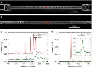
[image:3.595.113.486.442.651.2]solution for free-space interfaces in cavity quantum electro-dynamics. In particular, our design is optimized to be compatible with simultaneous fabrication of high-Q/Vresonators for quan-tum optics experiments, as we avoid additional fabrication steps31,32 that could impact the resonator performance. In this section, we therefore investigate coupling to the modes of nanophotonic resonators, which are used in quantum optics to enhance light-matter interactions41 and to facilitate efficient integration of quantum emitters into optical circuits. We study nanobeam photonic crystal (PhC) cavities, which host a TE mode
as shown in Fig. 3a, b. With a supercontinuum light source we
acquire the transmission spectra shown in Fig.3c by coupling a
free-space laser beam into the TE fundamental mode of the nanobeam and subsequently into PhC modes. The data in red correspond to the device with vertical couplers, while the black spectrum corresponds to a cavity with notches as the free-space interface for the same input power and integration time. The count rates of the device with notches as an interface are more than two orders of magnitude smaller, for which we compensate by integrating ten times longer (data in green). When comparing the cavity resonances (blue arrows), wefind a >550-fold increase in counts of the vertical coupler over the notch device for com-parable quality factors (Q≈4000). This result matches well with the 625-fold enhancement that we expect from simulations. This
improvement in coupling efficiencies allows for dramatically
decreased experimental times (in some cases from weeks to minutes of photon integration), thereby opening opportunities for larger-scale experiments. In Fig.3d we present spectra, where we couple the laser light directly to the cavity and optimize the alignment to collect maximum counts from the vertical coupler (red) and the notch (green). From this measurement, we can conclude that the extraction efficiency of light coupling from the cavity mode to the waveguide is≈24 times greater for a vertical
coupler than that for a notch, which corresponds well to the transmission experiment.
Inverse-designed diamond photonic circuit. For applications in quantum technologies, many nodes need to be connected to scale from single qubits to large, interconnected qubit arrays8,10,18.
This requires the excitation of emitters in multiple cavities, the interference of their emission on beamsplitters, and subsequently
the efficient collection and detection of photons. However, up
until now elements such as waveguide-splitters have posed a major challenge in suspended diamond photonics, as state-of-the-art fabrication using angled etch is not conducive to variations in
the device geometry. In contrast, as shown in Fig. 4a, we can
fabricate a conceptual circuit comprised of three components with completely different geometries: vertical couplers, wave-guide-splitters, and nanobeam PhC cavities. The device is designed to interfere the transmission of two nanobeam PhC cavities at an inverse-designed waveguide-splitter with a 50:50 splitting ratio and simulated efficiencies of 95%. We address the cavities separately or simultaneously by top-down excitation with a supercontinuum source focused on the cavities directly, as
presented in Fig. 4b. The resonances of the two beams are
detuned by <1 nm because of fabrication imperfections. We tune the two cavities into and out of resonance via gas condensation, as shown in Fig.4c. Comparing the amplitudes of the cavity on and off resonance suggests constructive interference, indicating that the cavities are approximately in phase and have the same polarization. With this concept circuit, we show that inverse design can overcome limitations of classical photonics and
enables large-scale on-chip quantum optics experiments.
Extending this work, we can increase compactness by combining several functionalities into a single device, design circuits for arbitrary emitter locations, assure phase-matching across
2 μm
2 μm
700 725 750 775 800 825
0.00 0.25 0.50 0.75 1.00
750 753 756 759
0.00 0.25 0.50 0.75 1.00
756 757 758 759 0.00
0.01 0.02 0.03 0.04
1x 10x
Counts (a.u.)
Wavelength (nm)
Grating coupler Notch Notch
1x
d
a
Grating coupler Notch
Counts (a.u.)
Wavelength (nm) c
b
[image:4.595.119.479.407.669.2]different paths of the circuits, and optimize for specific bandwidths. Such a platform can then utilize the scalability that diamond color centers offer: site-controlled implantation of high-quality color centers42,43and small inhomogeneous broadening44,
which can be overcome by cavity-enhanced Raman emission17,20
or strain tuning45–48.
Highly efficient free-space-waveguide interfaces. Ultimately the
implementation of scalable quantum networks requires effi
-ciencies of building blocks close to unity. Efficiencies of >90% can
be achieved with fiber tapers49, which have the drawback of
significantly larger footprints. To achieve comparable efficiencies,
we reduce the fabrication constraints to 60 nm feature sizes, increase the laser spot size, device footprint, and waveguide
width. This allows us to improve the simulated efficiency to
44.7%. However, vertically symmetric devices, such as shown in Fig.5a cannot exceed 50% efficiency. For further improvements, we tilt the incident laser beam by 10° and break the symmetry along thez-axis of the couplers via a partial etch32. In Fig.5b, we
show diamond devices on SiO2 with efficiencies of 51.0%. Such
devices could be achieved through diamond thin-film on SiO2
production5or pick and place techniques50and are a promising
route for a range of applications, including long-distance entan-glement schemes, and nonlinear optics. Devices suspended in air
2 μm a
746 748 750 752 754 756 758 0.0
0.5 1.0 1.5 2.0 2.5
3.0 760
758
1
0.8
0.6
0.4
0.2 756
Wavelength (nm) 754
752
100 200 300
Integration #
400 500 600
b
Counts (a. u.)
Wavelength (nm)
Upper beam Both beams Lower beam
c
Fig. 4Interfacing grating couplers with a diamond photonic circuit.aDiamond photonic circuit, which could be used to entangle two emitters inside the two cavities. The circuit consists of a grating coupler, followed by a waveguide-splitter, and two resonators, the outputs of which are then recombined in a waveguide-splitter and coupled off-chip through a grating coupler.bSpectra of the nanobeams from the device shown ina. Green, black, and red data correspond to the upper, both and the lower nanobeam, respectively.cDemonstration that cavities with fabrication induced frequency offset can be tuned in resonance via gas tuning; colorbar corresponds to normalized counts
100 a
f
b c d e
Efficiency (%)
80
60
40
20
0
a b c
Design Diamond 1 μm
SiO2 Air Aluminum
d e
Fig. 5Designs for high-efficiency vertical couplers.aVertically symmetric coupler suspended in air. Vertically asymmetric couplers employing partial etch with tilted incident laser beam (10°): vertical couplerbon SiO2,csuspended in air,don SiO2with aluminum back-reflector, andesuspended in air with
[image:5.595.119.479.51.243.2] [image:5.595.134.464.318.553.2](Fig. 5c) have a larger refractive index contrast and show effi -ciencies of up to 67.9%. Additionally employing back-reflectors31 as shown in Fig.5d, e results in efficiencies of 72.4% and 86.6%, for diamond on SiO2and suspended structures, respectively. The
back-reflector distance to the coupler (400 nm and 650 nm) is
significantly shorter than the photon wave-packet and optimized
to match the phase between reflected and directly coupled
pho-tons. These findings are encouraging for the development of
highly efficient and compact photonic free-space interfaces as an
alternative to fiber tapers for quantum photonic applications at
the single-photon level. Moreover, many experiments will require optical driving of individual emitters to compensate for their spectral broadening via Raman processes17,20. This individual
addressing is easier to implement in free-space coupling confi
g-urations than with many tapered fibers inside a cryostat. High
efficiencies and compactness will be crucial in these experiments, as losses will be the limiting factor. Thus, inverse design is likely to play a major role in the development of such photonic circuits30.
Discussion
In summary, we employ optimization-based inverse design methods to overcome the constraints of cutting-edge diamond nanofabrication and to develop efficient building blocks for dia-mond nanophotonic circuits51. In optical free-space couplers and a small diamond photonic circuit we attain the crucial properties
of high efficiency, compactness, and robustness. This work now
enables more complex quantum circuits, where compact solu-tions for a variety of device components such as pulse shapers, splitter trees, phase delays52, and mode converters53are critical.
Thus, this progress lays the foundation for scaling to larger
quantum networks8,10,54 with spins6 embedded in quantum
nodes. In addition, inverse design methods can be applied to other promising material platforms that host quantum emitters and have challenging fabrication protocols, such as silicon car-bide55and yttrium orthovanadate56.
Data availability
The data sets generated during and/or analyzed during this study are available from the corresponding authors on request.
Received: 28 March 2019 Accepted: 3 July 2019
References
1. Atatüre, M., Englund, D., Vamivakas, N., Lee, S. Y. & Wrachtrup, J. Material platforms for spin-based photonic quantum technologies.Nat. Mater.3, 38–51 (2018).
2. Awschalom, D. D., Hanson, R., Wrachtrup, J. & Zhou, B. B. Quantum technologies with optically interfaced solid-state spins.Nat. Photonics12, 516–527 (2018).
3. Khanaliloo, B. et al. Single-crystal diamond nanobeam waveguide optomechanics.Phys. Rev. X5, 041051 (2015).
4. Burek, M. J. et al. Diamond optomechanical crystals.Optica3, 1404–1411 (2015).
5. Hausmann, B. J. M., Bulu, I., Venkataraman, V., Deotare, P. & Loncar, M. Diamond nonlinear photonics.Nat. Photonics8, 369–374 (2014).
6. Rose, B. C. et al. Observation of an environmentally insensitive solid-state spin defect in diamond.Science361, 60–63 (2018).
7. Aharonovich, I., Greentree, A. D. & Prawer, S. Diamond photonics.Nat. Photonics5, 397–405 (2011).
8. Cirac, J. I., Zoller, P., Kimble, H. J. & Mabuchi, H. Quantum state transfer and entanglement distribution among distant nodes in a quantum network.Phys. Rev. Lett.78, 3221 (1997).
9. Briegel, H. -J., Dür, W., Cirac, J. I. & Zoller, P. Quantum repeaters: the role of imperfect local operations in quantum communication.Phys. Rev. Lett.81, 5932 (1998).
10. Kimble, H. J. The quantum internet.Nature453, 1023–1030 (2008). 11. Bernien, H. et al. Two-photon quantum interference from separate nitrogen
vacancy centers in diamond.Phys. Rev. Lett.108, 043604 (2012). 12. Sipahigil, A. et al. Quantum interference of single photons from remote
nitrogen-vacancy centers in diamond.Phys. Rev. Lett.108, 143601 (2012). 13. Bernien, H. et al. Heralded entanglement between solid-state qubits separated
by three metres.Nature497, 86–90 (2013).
14. Pfaff, W. et al. Unconditional quantum teleportation between distant solid-state quantum bits.Science345, 532–535 (2014).
15. Hensen, B. et al. Loophole-free Bell inequality violation using electron spins separated by 1.3 kilometres.Nature526, 682–686 (2015).
16. Gao, W. B., Imamoglu, A., Bernien, H. & Hanson, R. Coherent manipulation, measurement and entanglement of individual solid-state spins using optical
fields.Nat. Photonics39, 363–373 (2015).
17. Sun, S. et al. Cavity-enhanced Raman emission from a single color center in a solid.Phys. Rev. Lett.121, 083601 (2018).
18. Lemonde, M. A. et al. Phonon networks with silicon-vacancy centers in diamond waveguides.Phys. Rev. Lett.120, 213603 (2018).
19. Ladd, T. D. et al. Quantum computers.Nature464, 45–53 (2010). 20. Sipahigil, A. et al. An integrated diamond nanophotonics platform for
quantum-optical networks.Science354, 847–850 (2016).
21. Evans, R. E. et al. Photon-mediated interactions between quantum emitters in a diamond nanocavity.Science362, 662–665 (2018).
22. Balasubramanian, G. et al. Nanoscale imaging magnetometry with diamond spins under ambient conditions.Nature455, 648–651 (2008).
23. Degen, C. L., Reinhard, F. & Cappellaro, P. Quantum sensing.Rev. Mod. Phys.
89, 035002 (2017).
24. Burek, M. J. et al. High quality-factor optical nanocavities in bulk single-crystal diamond.Nat. Comm.5, 5718 (2014).
25. Khanaliloo, B., Mitchell, M., Hryciw, A. C. & Barclay, P. E. High-Q/V monolithic diamond microdisks fabricated with quasi-isotropic etching.Nano Lett.15, 5131–5136 (2015).
26. Mouradian, S., Wan, N. H., Schröder, T. & Englund, D. Rectangular photonic crystal nanobeam cavities in bulk diamond.Appl. Phys. Lett.111, 021103 (2017).
27. Wan, N. H., Mouradian, S. & Englund, D. Two-dimensional photonic crystal slab nanocavities on bulk single-crystal diamond featured.Appl. Phys. Lett.
112, 141102 (2018).
28. Mitchell, M., Lake, D. P. & Barclay, P. E. Realizing q > 300 000 in diamond microdisks for optomechanics via etch optimization.APL Photonics4, 016101 (2019).
29. Molesky, S. et al. Inverse design in nanophotonics.Nat. Photonics12, 659–670 (2018).
30. Su, L. et al. Fully-automated optimization of grating couplers.Opt. Express26, 4023–4034 (2018).
31. Van Laere, F. et al. Compact and highly efficient grating couplers between opticalfiber and nanophotonic waveguides.J. Light. Technol.25, 151–156 (2007).
32. Vermeulen, D. et al. High-efficiencyfiber-to-chip grating couplers realized using an advanced CMOS-compatible silicon-on-insulator platform.Opt. Express18, 18278–18283 (2010).
33. Rath, P., Khasminskaya, S., Nebel, C., Wild, C. & Pernice, W. H. Grating-assisted coupling to nanophotonic circuits in microcrystalline diamond thin
films.J. Light. Technol.4, 300–305 (2013).
34. Faraon, A. et al. Quantum photonic devices in single-crystal diamond.New J. Phys.15, 025010 (2013).
35. Piracha, A. H. et al. Scalable fabrication of integrated nanophotonic circuits on arrays of thin single crystal diamond membrane windows.Nano Lett.16, 3341–3347 (2016).
36. Zhou, X. et al. High-efficiency shallow-etched grating on GaAs membranes for quantum photonic applications.Appl. Phys. Lett.113, 251103 (2018). 37. Gould, M., Schmidgall, E. R., Dadgostar, S., Hatami, F. & Fu, K. -M. C. Efficient
extraction of zero-phonon-line photons from single nitrogen-vacancy centers in an integrated gap-on-diamond platform.Phys. Rev. Appl.6, 011001 (2016). 38. Piggott, A. Y. et al. Inverse design and implementation of a wavelength
demultiplexing grating coupler.Sci. Rep.4, 7210 (2014).
39. Lu, J. & Vuckovic, J. Nanophotonic computational design.Opt. Express21, 13351–13367 (2013).
40. Piggott, A. Y., Petykiewicz, J., Su, L. & Vučković, J. Fabrication-constrained nanophotonic inverse design.Sci. Rep.7, 1786 (2017).
41. Zhang, J. L. et al. Strongly cavity-enhanced spontaneous emission from silicon-vacancy centers in diamond.Nano Lett.18, 1360–1365 (2018). 42. Evans, R. E., Sipahigil, A., Sukachev, D. D., Zibrov, A. S. & Lukin, M. D.
Narrow-linewidth homogeneous optical emitters in diamond nanostructures via silicon ion implantation.Phys. Rev. Appl.5, 044010 (2016).
44. Rogers, L. et al. Multiple intrinsically identical single-photon emitters in the solid state.Nat. Commun.5, 4739 (2014).
45. Meesala, S. et al. Enhanced strain coupling of nitrogen-vacancy spins to nanoscale diamond cantilevers.Phys. Rev. Appl.5, 034010 (2016). 46. Meesala, S. et al. Strain engineering of the silicon-vacancy center in diamond.
Phys. Rev. B97, 205444 (2018).
47. Sohn, Y. -I. et al. Controlling the coherence of a diamond spin qubit through its strain environment.Nat. Commun.9, 2012 (2018).
48. Machielse, B. et al. Quantum interference of electromechanically stabilized emitters in nanophotonic devices.Preprint athttp://arXiv.org/abs/1901.09103
(2019).
49. Burek, M. J. et al. Fiber-coupled diamond quantum nanophotonic interface.
Phys. Rev. Appl.8, 024026 (2017).
50. Kim, J. -H. et al. Hybrid integration of solid-state quantum emitters on a silicon photonic chip.Nano. Lett.17, 7394–7400 (2017).
51. O’Brien, J. L., Furusawa, A. & Vučković, J. Photonic quantum technologies.
Nat. Photonics3, 687–695 (2009).
52. Vampa, G., Fattahi, H., Vuckovic, J. & Krausz, F. Attosecond nanophotonics.
Nat. Photonics11, 210–212 (2017).
53. Lu, J. & Vučković, J. Objective-first design of high-efficiency, small-footprint couplers between arbitrary nanophotonic waveguide modes.Opt. Express20, 7221–7236 (2012).
54. Wehner, S., Elkouss, D. & Hanson, R. Quantum internet: a vision for the road ahead.Science362, 6412 (2018).
55. Koehl, W. F., Buckley, B. B., Heremans, F. J., Calusine, G. & Awschalom, D. D. Room temperature coherent control of defect spin qubits in silicon carbide.
Nature479, 84–87 (2011).
56. Zhong, T. et al. Nanophotonic rare-earth quantum memory with optically controlled retrieval.Science357, 1392–1395 (2017).
Acknowledgements
We acknowledge the help of Usha Raghuram and Elmer Enriquez with RIE. This work is
financially supported by Army Research Office (ARO) (award no. W911NF1310309), Air Force Office of Scientific Research (AFOSR) MURI Center for Attojoule Nano-Optoelectronics (award no. FA9550-17-1-0002), National Science Foundation (NSF) Division Of Electrical, Communications Cyber Systems (ECCS) (award no. 1838976), and Gordon and Betty Moore Foundation; C.D. acknowledges support from the Andreas Bechtolsheim Stanford Graduate Fellowship and the Microsoft Research Ph.D Fellow-ship. K.Y.Y. and M.R. acknowledge support from the Nano- and Quantum Science and Engineering Postdoctoral Fellowship. D.M.L. acknowledges support from the Fong Stanford Graduate Fellowship. D.M.L. and A.E.R. acknowledge support from the National Defense Science and Engineering Graduate (NDSEG) Fellowship Program, sponsored by the Air Force Research Laboratory (AFRL), the Office of Naval Research (ONR) and the Army Research Office (ARO). D.V. acknowledges funding from FWO and European Unions Horizon 2020 research and innovation program under the Marie Sklodowska-Curie grant agreement No. 665501. We thank Google for providing
computational resources on the Google Cloud Platform. Part of this work was performed at the Stanford Nanofabrication Facility (SNF) and the Stanford Nano Shared Facilities (SNSF), supported by the National Science Foundation under award ECCS-1542152.
Author contributions
C.D. and J.V. conceived and designed the experiment. C.D. developed the fabrica-tion techniques, fabricated the sample, and measured and analyzed the data. D.V., N.V.S., C.D., and L.S. conducted inverse design optimization of photonic components. K.Y.Y., D.M.L., and A.Y.P. contributed to the sample fabrication. A.E.R. and S.S. con-tributed to optical measurements. J.L.Z., M.R., and K.G.L. provided expertize. J.V. supervised the project. All authors participated in the discussion, understanding of the results, and the preparation of the manuscript.
Additional information
Supplementary Informationaccompanies this paper at https://doi.org/10.1038/s41467-019-11343-1.
Competing interests:The authors declare no competing interests.
Reprints and permissioninformation is available online athttp://npg.nature.com/ reprintsandpermissions/
Peer review information:Nature Communicationsthanks Tian Zhong and the other
anonymous reviewer(s) for their contribution to the peer review of this work. Peer reviewer reports are available.
Publisher’s note:Springer Nature remains neutral with regard to jurisdictional claims in published maps and institutional affiliations.
Open Access This article is licensed under a Creative Commons
Attribution 4.0 International License, which permits use, sharing, adaptation, distribution and reproduction in any medium or format, as long as you give appropriate credit to the original author(s) and the source, provide a link to the Creative Commons license, and indicate if changes were made. The images or other third party material in this article are included in the article’s Creative Commons license, unless indicated otherwise in a credit line to the material. If material is not included in the article’s Creative Commons license and your intended use is not permitted by statutory regulation or exceeds the permitted use, you will need to obtain permission directly from the copyright holder. To view a copy of this license, visithttp://creativecommons.org/ licenses/by/4.0/.