RECENT DEVELOPMENTS IN FIBRE TECHNOLOGY AND ITS APPLICATION WITHIN HIGH SPEED OPTICAL COMMUNICATIONS
D.J. Richardson, J.Y.Y. Leong, F. Parmigiani, P.J. Almeida, M. Ibsen, P. Petropoulos
Optoelectronics Research Centre University of Southampton, UK Phone:+44 2380 594524, Fax+44 2380 593142
ABSTRACT
Recent advances in optical fibre technology, most notably in the area of microstructured fibres, high power rare-earth doped fibres, and superstructured fibre Bragg gratings offer a host of new opportunities within future high speed communication systems. Herein we review the increased range of waveguide characteristics that can now be obtained within fibre with an emphasis on both fibre nonlinearity and dispersion control, and describe the latest advances in the design and fabrication of fibre Bragg gratings for the manipulation and shaping of ultrashort pulses. We then outline how such components can be integrated into various all-optical processing devices for high speed optical communication systems focusing in particular on data retiming and OTDM add-drop multiplexing.
1. INTRODUCTION
The development of low loss, dispersion optimised transmission fibres coupled with the development of the erbium doped fibre amplifier has revolutionized telecommunications. Tbit/s data capacity transmission over transoceanic distances can now be routinely achieved using DWDM technology [1], and single channel data rates of >2.5Tbit/s over ~160km have also now been demonstrated [2]. In order to fully exploit this inherent transmission capacity within networks, the use of all-optical processing techniques such as optical regeneration, wavelength conversion and routing will ultimately be required. It looks likely that fibre technology could play a critical role here also, both in terms of pulse shape control and in terms of providing an ultrafast nonlinear optical element. In this paper we review recent developments in nonlinear fibre fabrication with a primary emphasis on microstructured fibre technology. We then briefly outline the state-of-the-art in terms of fibre grating for pulse shaping applications, and conclude by describing the operation and performance of two elementary pulse
processing systems that we believe highlight the potential of combining these two enabling technologies for optical processing applications.
2. NONLINEAR FIBRES
The effective nonlinearity-per-unit-length γ of a
fibre at a wavelength λ is given by γ = 2π n2 / (λAeff)
where n2 is the nonlinear refractive index of the glass
and Aeff is the effective area of the fibre. In order to
control γ one can in practice either control the value
of n2 through material choice, and/or change Aeff. The
extent to which Aeff can be controlled is ultimately
defined by the index contrast between core and cladding materials, which can be quite limiting in the case of conventional solid fibre fabrication. Finding suitable thermally and optically matched materials for core and cladding severely limits the range of high n2
materials that can be used for conventional solid fibres.
2.1 Conventional solid HNLFs
By moving to materials with a higher intrinsic nonlinearity, e.g. bismuth based glasses, it is possible to achieve far higher values of γ, albeit with increased losses. For example, values as high as γ = 1000 W
-1
km-1 with losses ~1dB/m have been achieved in Bismuth doped fibre, and again these fibres are now commercially available [5]. However, it is to be appreciated that it is not possible to achieve zero dispersion wavelength at 1550nm due to the high material dispersion of bismuth based glasses at these wavelengths. This is due to the limited index contrasts that can be achieved using suitable combinations of glass for core and cladding.
2.2 Microstructured fibres
Microstructured fibre technology allows the possibility to benefit from the large linear and nonlinear refractive index contrasts between glass and air to realize fibres with truly unique and useful properties. By suitable control of the fibre transverse structure, and material choice, it is possible to envisage fibre designs with nonlinearities that are tailorable over more than 7-orders of magnitude [6]. This opens up a host of new device possibilities ranging from nonlinear elements for telecommunications applications through to low nonlinearity fibres for high power laser delivery.
In the low nonlinearity extreme we estimate that low loss PBG fibres (see Fig.1a) with nonlinearities around 1000 times lower than existing SMF should be possible, by minimizing the amount of light propagating within the solid regions of the fibre, and maximizing the amount of light within the low nonlinearity air core. At the other extreme we can anticipate HFs with nonlinearities that are 10,000 times that of conventional SMF by making use of both the tight mode confinement possible in small-core, high-NA HF and the large material nonlinearities that can be achieved in high index materials such as chalcogenide glass. Nonlinearities approaching the maximum theoretical values possible in fibre form have now been achieved for several materials. For example, γ values at 1550nm of 70 W
-1
km-1and 1860 W-1km-1 have been achieved in pure silica (see Fig.1c) [7] and lead silicate HFs (see Fig.1d) [8] respectively. Note that once such high levels of nonlinearity can be achieved, e.g. to the point that devices of order 1m become practical, then the relatively high losses (~1dB/m) of high-index base materials cease to be a major limiting issue for many important applications.
Whilst this is in itself an impressive achievement,
obtaining suitable dispersion properties is often of greater importance for many nonlinear device applications, necessitating a trade-off in magnitude of nonlinearity for dispersion control. The high index contrast between air and glass allows for extreme values of waveguide dispersion and this can be used to control the large material dispersion associated with compound glasses at wavelengths of interest in the near IR – e.g. at 1550nm for telecommunications, or around 1060nm for incorporation within Yb-doped fibre based devices.
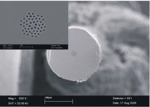
In Fig.2 we show a lead silicate HF with a hexagonal arrangement of effectively 4 rings of holes (48 holes in total), produced by stacking together just 7 structured elements [9]. As opposed to our previously extruded suspended-core HFs [8], whose critical properties are determined primarily by just one parameter, the core diameter, these SEST fibres have two adjustable parameters: the hole-to-hole pitch Λ and the hole diameter d (or relative hole size d/Λ). Λ is adjusted by the scale of the microstructured region. Note that the core size of the SEST fibres depends on both d and Λ, and is about 2Λ-d. The core size of the HF shown in Fig.2 was varied between 2.4-4.5 µm and had a d/Λ ratio of 0.48 in the outer cladding region, and 0.55 in the region surrounding the core. The loss of these early SEST fibres is around 3dB/m, although losses below 1dB/m are ultimately expected for this glass type.
The great advantages of SEST HFs though can be appreciated when the fibre dispersion is considered.
(a) (b)
(c) (d)
(a) (b)
(c) (d)
We have performed numerical simulations using a full vector model to calculate the group velocity dispersion (GVD) profiles of the 3 SEST fibres so far produced. In Fig.3 we plot the theoretical variation of dispersion with wavelength for our three fibre samples. HF #2 and #3 are seen to exhibit anomalous GVD throughout the C-band due to an excess of waveguide dispersion in this region. However, for HF #1 the effects of material and waveguide dispersion oppose each other in such a way that the zero-dispersion wavelength is shifted to the region between 1530-1540nm, as intended from our design calculations. We also plot theoretical dispersion profiles of several extruded SF57 suspended-core fibres previously fabricated with maximum nonlinearity in mind [8]. The primary zero dispersion wavelength for these fibres lies around 1µm. The figure shows that the SEST designs offer far greater control and flatter dispersion profiles in the 1.55µm region compared to the suspended-core structures previously fabricated. Fig.3 also shows the dispersion profile of a theoretical SEST design optimised for flattened dispersion at 1.55µm which highlights the excellent properties that should ultimately be achievable using the SEST approach [10].
Fig.2 SEM image of the dispersion shifted SEST fibre at 1.55µm (HF#1).
W a v e le n g th ( u m )
0. 8 1 .0 1. 2 1 .4 1. 6 1 .8 2 .0
D
is
p
e
rs
io
n
(
p
s
/n
m
/k
m
)
-1 0 0 0 1 0 0 2 0 0
0 .7 u m c o re H N L F -S F 5 7 1 .0 u m c o re H N L F -S F 5 7 [re f. 3] S F 5 7 bu l k gl as s O pti m is e d S E S T H F 1 H F 2 H F 3
H F # 3
H F # 2 H F # 1
Fig.3 Comparison of dispersion profiles of our previous work on suspended-core HFs with different core sizes and various SEST fibres including an optimised design offering reduced dispersion slope. The nonlinearities of these three fibres were 170,250,410 W-1Km-1 for HF1, HF2 and HF3 respectively.
2.3 Pulse shaping using SSFBGs
Fibre Bragg grating technology has now advanced to the point that gratings with truly complex phase and amplitude reflectivity profiles can be reliably designed, and fabricated [11]. It is thus possible to produce gratings designed to reshape optical pulses suited for a given optical communications function. To date pulse shaping gratings have been most commonly used for dispersion compensation applications, but interest is now growing in using such devices for a host of optical processing applications, including optical code generation and recognition, timing jitter tolerant optical demultiplexing [12] and pulse repetition rate multiplication [13]. In the following section we present data on a pulse reshaping grating designed to generate parabolic shaped pulses from incident soliton pulses as reliably generated from a mode-locked fibre laser. Parabolic pulses are of great interest for applications such as all-optical Fourier transformation, optical regeneration and high power pulse amplification schemes amongst others.
3. EXAMPLES OF OPTICAL PROCESSING USING HNLF’S AND SSFBG’S
3.1 Timing Jitter reduction
Timing jitter reduction is likely to be an essential function within future high speed optical communication systems. Here we present a technique for drastically reducing timing jitter induced in short pulse transmission systems based on the use of Cross-Phase Modulation (XPM) in a HNLF [14].
The experimental set-up and the retiming scheme principle are shown in Fig.4. The technique is based on the fact that the frequency-shift imparted by an
4KHz
EDFA EFRL
λο=1542nm
Pulse Shaping SSFBG FM
Gain Switched DFB
λ=1556nm Co
m
p
re
ss
io
n
st
ag
e
10GHz
~
10Gbit/s
231-1 PRBS
Generator MOD
Delay line
HNLF 220m
t
t
/ /
~ ~ ~
λo=1556nm
CW
t
SMF 500m t
[image:3.595.107.262.379.490.2]intense control pulse on a co-propagating signal in a Kerr medium is given by:
,
)
(
2
)
(
2
T
T
T
U
L
P
T
T
o eff∂
∆
−
∂
−
=
∂
∂
−
=
φ
γ
δω
where γ and Leff are the nonlinear coefficient and the
effective length of the HNLF respectively, Po is the
control peak power, U(T) is the normalized slow varying amplitude of the pulse envelope, and ∆T is the initial relative time delay between the signal and the control pulse. Thus if the control signal has a well defined clock rate and comprises pulses with a parabolic intensity profile then we can use this time derivative effect to impart a frequency shift on individual pulses within an incident data stream that is simply proportional to the temporal offset of the data pulses from the control pulse centre. There is thus a one-to-one linear mapping of timing jitter to frequency jitter. By passing the frequency modulated data bits through a suitably dispersive delay line, it is possible to retime the data bits on a bit-by bit basis. The key issue with this technique is how to produce the control pulses with a sufficiently accurate parabolic pulse shape. Here we show that this is possible using a simple grating based pulse shaper.
Fig.5 (Left) Experimental (dotted line) and calculated (dashed-dotted line) spectrum of the parabolic pulses. Fig.6 (Right) Intensity of the shaped parabolic pulses measured using SHG-FROG and its corresponding gradient.
A mode-locked erbium fibre ring laser (EFRL) operating at 1542nm is used to generate ~2 ps soliton pulses at a repetition rate of 10 GHz. These pulses are used as the input to the parabolic pulse shaper. The shaped pulses are designed to have a parabolic envelope (FWHM of ~10 ps) superimposed upon a 5th order super-Gaussian profile which is used to smoothen the pulse edges and reduce its spectral extent. The grating was designed and fabricated with an appropriate phase and amplitude response to convert the 2 ps solitons into the target parabolic pulses. The measured optical spectrum of the pulses from the SSFBG is shown in Fig.5 (dotted line)
together with the theoretically calculated single parabolic pulse spectrum (dashed-dotted line). As can be seen, we can accommodate 11 spectral lobes with an excellent agreement, highlighting the quality of our grating writing process. A detailed assessment of the quality of the parabolic pulses is carried out before processing with our retiming experiment. We characterised the pulses reflected off the SSFBG using second harmonic generation frequency-resolved optical gating (SHG-FROG) and calculated the time derivative of their intensity profile, as seen in Fig.6. As can be seen, this derivative exhibits a good linear slope across the 10 ps pulsewidth.
Fig.7 Output versus input rms timing jitter of the data signal (Inset) Eye diagrams before (a.1-3) and after (a.4-6) the retiming scheme for three different values of induced timing jitter: rms~1.8ps p~10.4ps), rms~2.9 (p-p~15.3ps) and rms~3.5ps (p-p~16.4ps). Time scale: 10ps/div.
The data source, synchronised to the EFRL signal, was a gain-switched Distributed Feedback (DFB) laser, operating at 1556nm. The pulses were compressed down to ~2ps using 125m of DCF followed by a nonlinear compression stage. The pulses were then modulated by a 231-1 pseudorandom bit sequence using a lithium niobate modulator and fed into 220m of HNLF (γ ~20W-1km-1) by a 90-10 splitter. The HNLF has a zero-dispersion wavelength at 1550nm, which ensured minimum walk-off time between the two signals. An optical delay line was used to temporally overlap the two signals. The data signal was then filtered using a 5 nm broadband optical filter and then launched into 500 m of SMF as required to remove the chirp, and thus to retime the pulses. We artificially introduce timing jitter on the data pulses by frequency modulating the 10 GHz RF
Input Timing Jitter RMS [ps]
0 1 2 3 4
O
u
tp
u
t
T
im
in
g
J
it
te
r
R
M
S
[
p
s
]
0 1 2 3
4 (a1) (a2) (a3)
drive signal of the laser with a 4 kHz tone. The amount of induced timing jitter could be changed by varying the amplitude of the frequency modulation.
We evaluated the quality of our retiming scheme at the system output for several values of timing jitter deliberately applied to the incident data pulses. These measurements are summarised in Fig.7, where we also show examples of eye diagrams at the input and output of the retiming scheme, obtained for incoming signals which have an rms timing jitter of ~1.8 ps ((peak-peak (p-p) of ~10.4 ps), ~2.9 ps ( p-p of ~15.3 ps) and ~3.5 ps ( p-p of ~16.4 ps) respectively. The measured jitter of the pulses at the output of the retiming scheme cases was measured as ~1 ps (RMS value) – the resolution limit of the sampling scope used for our measurements.
3.2 Add drop multiplexing
Time division add-drop multiplexing (TADM) is likely to become a key function in future ultra-high-speed optical communications. TADM has been demonstrated by various groups based on the dropping of channels directly within the time domain using a fast optical switch. However the reported values of suppression ratio between the through and cleared channels is typically less than 25-dB and is limited by the finite extinction ratio of the switch. This severely limits the cascadability of such devices. Here we demonstrate a TADM approach capable of providing a 35-dB channel suppression ratio based on OTDM to WDM format conversion [15].
Our scheme is shown in Fig.8. The incoming OTDM signal is used to sample a chirped optical pulse thereby generating a mixed TDM-WDM representation of the incident OTDM signal. Each tributary channel is mapped onto a separate WDM channel which allows further processing of the signal within the frequency domain. (Additional time domain processing can also be performed at this stage if required). Since we are using linearly chirped
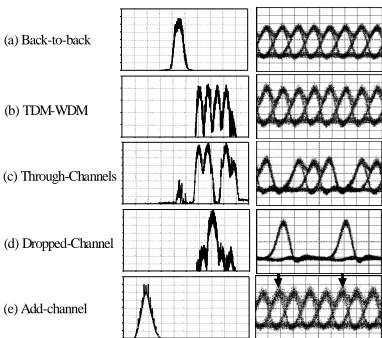
pulses and a 1:1 mapping exists between the time and wavelength domains this allows us to use high extinction ratio filters, (high precision fibre gratings in our case), to obtain high extinction ratio channel drops when we convert the intermediate TDM-WDM signal back to an OTDM signal at the TADM output. The temporal windows of the through and drop ports are dependent on the linear chirp rate of the mapping pulses. For our particular system, where we have used mapping pulses with a linear chirp rate of 6 nm over 100 ps, the 1.5 nm bandwidth of the FBG corresponds to a switching window of 25 ps (Fig.9). For reference, the spectral traces shown in the figure were taken with a resolution of 0.01 nm which corresponds to a temporal resolution of 170 fs. These traces also show that the FBG had a minimum side lobe extinction of 24 dB in reflection and a transmission loss at of 35 dB at the peak of the reflectivity curve. The channel suppression is calculated by integrating the power within the timeslot before and after the through port. In this case we obtained 33dB across the full-width at half-maximum of the dropped channel.
The OTDM data pulses were generated using a gain-switched diode laser producing 9-ps pulses at a repetition rate of 10-GHz and a central wavelength of 1546-nm. They were modulated externally with a
231-1 PRBS and multiplexed to a line rate of
40Gbit/s.
Wavelength (nm)
1549 1550 1551 1552 1553 1554
T
ra
n
sm
is
si
o
n
(5
d
B
/d
iv
)
Time delay (ps)
0 25 50 75
24-dB 35-dB
100 Through
Dropped
Fig.10(a) shows the corresponding spectrum and eye diagram. At the add-drop multiplexer input the 40 Gb/s data was amplified to an average power of 20-dBm and launched into the control port of a highly-nonlinear fibre optical loop mirror (HNLF-NOLM). The signal to the HNLF-NOLM comprised 100-ps linearly-chirped rectangular pulses at a 10-GHz repetition rate and highly flat top bandwidth of 6-nm. At the HNLF-NOLM output the control pulses were filtered out and a TDM-WDM replica of the original data was carved onto the chirped pulses, Fig. 10(b). Each channel -3dB bandwidth was 0.7-nm and the spacing between them 1.4-nm. The TDM-WDM signal was then transmitted through the tunable fibre Bragg grating (FBG) add/drop multiplexer using the circulator arrangement shown in Fig.8. The drop port was then port 3 of C1 and the add port of a new 10-Gb/s channel was port 1 of C2. Fig. 10(c) and (d) show the spectra and eye diagrams of the through and dropped channels respectively. Rather than using a new pulse source we chose to re-inject the dropped signal through the add port. Note that this case represents the worst case in terms of coherent interference with the previously dropped channel. The second HNLF-NOLM was used to convert the mixed TDM-WDM signal back to a single wavelength 40 Gb/s TDM signal. The polarizer was inserted to equalize the SOP of all channels at the input of the second NOLM switch. The TDM-WDM signal was then amplified to an average power of 18-dBm and used as the NOLM control to switch a continuous-wave beam at 1541-nm. At the output of the NOLM a 1.3-nm band-pass filter isolated the switched signal from the control, as shown in Fig. 10(e). The final resulting signal was characterised using a 40 Gb/s receiver consisting of a 40:10 Gb/s
electro-absorption modulator-based demultiplexer. Error-free operation was achieved within a 2-dB power penalty for all cases, and no degradation due to crosstalk was observed for the added channel. Finally we tested the simultaneous dropping of two channels in a proof-of-principle demonstration using the two grating arrangement of Fig.11. The eye diagrams that we obtained are shown in the same figure.
TFBG 1 2
3 TFBG 2
2 1
3 1
drop ch.1 drop ch.2
[image:6.595.78.269.75.244.2]back-to-back WADM Through-Channels
Fig.11 Simultaneous multiple channel drop.
4. CONCLUSIONS
In conclusion we have reviewed recent progress in the area of both nonlinear fibre and SSFBG fabrication. We have shown that by combining these two enabling technologies it is possible to perform a range of ultrafast all-optical processing functions in a relatively simple and straightforward manner. We consider our results to highlight that this a most promising approach to manipulating and controlling optical signals within future optical networks.
REFERENCES
[1] G. Charlet et al., paper PDP 36, OFC 2004. [2] H.G. Weber et al, Th4.1.2, Proc. ECOC 2005. [3] M. Takahashi et al. paper We4.P019, Proc
ECOC 2004.
[4] M. Hirano et al., PD paper Th4.4.4, Proc ECOC 2005.
[5] K. Kikuchi, K. Taira, N. Sugimoto, Electron. Letts, 38, pp166-167, 2002.
[6] D.J. Richardson et al., Proc IEEE WFOPC 2005.
[7] V. Finazzi, T.M.Monro, D.J.Richardson, J. Opt. Soc. Am. B, 20, pp1427-36 (2003).
[8] J.Y.Y. Leong et al. Paper PDP22, OFC 2005. [9] J.Y.Y. Leong et al. PD paper Th4.4.5, proc
ECOC 2005.
[10] F. Poletti et al., Opt. Exp., 13, pp.3728-373, 2005.[
11] M. Ibsen et al., IEEE Photon. Technol. Letts, 10, pp.842-4, 1998.
[12] J.H. Lee et al., IEEE Photon. Technol. Letts, 14, pp.203-5, 2002.
[13] P. Petropoulos et al., Opt. Letts. , 25, pp.521-3, 2001.
[image:6.595.319.535.183.223.2][14] F. Parmigiani et al., Paper Tu4.6.4, ECOC 2005 [15] P. J. Almeida et al., Paper OWW3, OFC 2006.
Fig. 10 Left: Optical spectrum (1537-1557nm) (5 dB/div, 2 nm/div, 0.01-nm resolution). Right: Eye diagrams.
W a v e l e n g t h ( n m ) 1 5 3 71 5 3 91 5 4 11 5 4 31 5 4 51 5 4 71 5 4 91 5 5 11 5 5 31 5 5 51 5 5 7
P
o
w
e
r
(
d
B
m
)
- 5 0 - 4 5 - 4 0 - 3 5 - 3 0 - 2 5 - 2 0 - 1 5 - 1 0
W a v e l e n g t h ( n m ) 1 5 3 71 5 3 91 5 4 11 5 4 31 5 4 51 5 4 71 5 4 91 5 5 11 5 5 31 5 5 51 5 5 7 - 4 0
- 3 5 - 3 0 - 2 5 - 2 0 - 1 5
W a v e l e n g t h ( n m ) 1 5 3 71 5 3 91 5 4 11 5 4 31 5 4 51 5 4 71 5 4 91 5 5 11 5 5 31 5 5 51 5 5 7
P
o
w
e
r
(
d
B
m
)
- 6 5 - 6 0 - 5 5 - 5 0 - 4 5 - 4 0 - 3 5 - 3 0 - 2 5
Wave le ng t h ( nm ) 15 37 1 539 1 54 1 154 3 15 45 1 54 7 1 54 9 155 1 15 53 15 5 5 1 55 7
P
o
w
e
r
(d
B
m
)
- 6 5 - 6 0 - 5 5 - 5 0 - 4 5 - 4 0 - 3 5 - 3 0 - 2 5
15 3 7 1 53 9 15 4 1 15 4 3 1 54 5 15 4 7 15 4 9 1 5 51 15 5 3 15 5 5 1 5 57 - 59
- 54 - 49 - 44 - 39 - 34 - 29 - 24 - 19
(a) Back-to-back
(b) TDM-WDM
(d) Dropped-Channel