Int. J. Electrochem. Sci., 9 (2014) 2985 - 2992
International Journal of
ELECTROCHEMICAL
SCIENCE
www.electrochemsci.org
Preparation and Characterization of CZTSe Films through
Electrochemical Deposition Route
Tung-Cheng Liu, Yi Hu*
Department of Materials Engineering, Tatung University, Taipei, Taiwan; No. 40, Sec. 3, Zhongshan N. Rd., Taipei City 104, Taiwan (R. O. C.)
*
E-mail: huyi@ttu.edu.tw
Received: 28 January 2014 / Accepted: 5 March 2014 / Published: 23 March 2014
Single-step electrochemical deposition of Cu2ZnSnSe4 (CZTSe) films without selenization was
reported. The CZTSe films were deposited potentionstatically on molybdenum substrate from an aqueous solution with CuSO4, ZnSO4, SnSO4 and H2SeO3 at room temperature. The chemical
composition, crystalline phase, morphology and optical properties of the CZTSe films have been studied using x-ray photoelectron spectroscopy (XPS), x-ray diffraction technique (XRD), Raman scattering spectrum, field emission scanning electron microscope (FE-SEM) and optical absorption techniques. The results showed that the content of Cu/Zn ratio decreased in the composition as the ectrodeposition voltage increased. The direct band gaps of the films are found to be about from 1.22 to 1.36 eV dependent of the composition variation. The film has higher direct band gap with lower Cu/(Zn+Sn) ratio in composition.
Keywords: Cu2ZnSnSe4; electrochemical deposition; solar cell absorber.
1. INTRODUCTION
Thin film solar cells, such as Cu(In,Ga)Se2 (CIGS) solar cell, have attracted much attention for
its power conversion efficiency over 20% at the laboratory level [1]. However, the materials for CIGS thin film solar cell such as In and Ga are rare, expensive and to hinder their commercialization. Therefore, the research about the new material device to substitute the CIGS, such as Cu2ZnSnSe4
(CZTSe), are carried out [2]. The materials for CZTSe are low cost, less toxic, earth abundant, and suitable to be applied for thin film solar cell absorber.
CZTSe is an I2-II-IV-VI4 quaternary p-type semiconductor obtained by replacing half of
indium by zinc and other half by tin in CuInSe2 chalcopyrite ternary compound[3]. It has a suitable
region for application of solar cell[4]. Because of these optical characteristics, the theoretical power conversion efficiency of CZTSe enables to 32.2 % according to Shockley-Quseisser theory [5].
CZTSe as an absorption layer for solar cells were first reported with 0.66 % power conversion efficiency for the vacuum-deposited technique by Katagiri et al in 1997 [2]. In last decades, many techniques for growth of CZTSe films have been adopted. CZTSe films can be obtained from conventional nonsolution techniques including co-evaporation and sputtering technique [2, 6-9]. On the other hand, it can also be obtained from solution route, such as electrodeposition [10, 11], and spin coated [12, 13], etc. Among these methods, electrodeposition is an attractive technique used for the low cost preparation of semiconductor thin films. The electrodeposition method has some advantages, such as low-cost preparation equipment, large area deposition, room temperature growth and easy to control the composition and morphology of the films. There have some report on fabrication of CZTSe films from electrodeposition method. Xu et al. reported an approach to fabricate CZTSe films by preparing Cu-Zn-Sn-Se precursors via one-step co-electroplating method, and they annealed the CZTSe precursor films in selenium vapors to form the CZTSe films[10]. Ikeda at al. fabricated the CZTSe films by electrodeposition and then sulfurization to fabricate quinary CZTSSe films[11]. Both of these reports needed selenization or sulfurization to form CZTSe films or CZTSSe films. In this work, we fabricated CZTSe films by a single-step electrochemical deposition process without selenization. The effect of various deposited potentials on the compositional, structural and morphological characteristics of the CZTSe films was investigated.
2. EXPERIMENTAL DETAILS
The Cu2ZnSnSe4 (CZTSe) films were potentionstatically deposited on molybdenum substrate
with an aqueous electrolytic bath containing 0.02 M copper (II) sulfate (CuSO4), 0.01 M zinc sulfate
(ZnSO4), 0.04 M tin sulfate (SnSO4), 0.06M selenious acid (H2SeO3) and 0.02 M sodium thiosulfate
(Na2S2O3) for 40 minutes at room temperature. 0.2 M tri-sodium citrate (C6H5Na3O7) and 0.1 M
tartaric acid (C4H6O6) solution were used as complexing agents. A standard three electrodes system
was employed. A molybdenum substrate, a platinum (Pt) foil and a saturated calomel electrode (SCE) were used as the working electrode, the counter electrode and the reference electrode, respectively. The films were deposited at -0.9, -1.0 -1.1 and -1.2 V, which were respect to the SCE reference electrode. The deposition area of the working electrode was 1 cm2 by controlling the depth of immersion in the electrolyte.
The states of the ions of the samples were measured using an X-ray photoelectron spectroscopy (XPS, Thermo VG-Scientific, Sigma Probe) with Al-Kα X-ray (E=1486.6 eV) as the excitation source.
High-resolution scans were performed with a pass energy of 50 eV and a step size of 0.10 eV/step. All spectra were shifted to account for sample charging using inorganic carbon as a reference to 285 eV. The crystalline characterization of the films were studied by X-ray diffractometer (XRD, PANalytical, X’Pert PRO MPD) with Cu-Kα radiation (λ=1.541838 Ǻ), and the scanning range was between 2θ=10
scanning electronic microscope (FESEM, Hitachi, S-4700I) under 15 kV operating voltage. The measurements of UV-Vis absorption were conducted by the equipment of UV-VIS JASCO V-560 with wavelength range from 350 to 800 nm.
3. RESULTS AND DISCUSSION
Figure 1. XPS spectra of (a) Cu(2p3/2, 2p1/2), (b) Zn(2p3/2), (c) Sn(3d5/2) and (d) Se(3d5/2) of CZTSe
films versus deposition potential: (1) V=-0.9, (2) V=-1.0, (3) V=-1.1, (4) V=-1.2.
Figure 1 shows the X-ray photoelectron spectroscopy (XPS) spectra of Cu(2p3/2, 2p1/2),
Zn(2p3/2), Sn(3d5/2) and Se(3d5/2) of the films versus the deposition potential. The Cu 2p3/2 and Cu
[image:3.596.70.524.176.647.2]
spectra are indicative of monovalent copper, Cu(I), existing in the film. The results showed that the binding energies were 932 and 952 eV for Cu 2p3/2 and Cu 2p1/2, respectively, and was in good
agreement to the values reported for Cu(I) [14]. The binding energy of Zn 2p3/2, Sn 3d5/2 and Se 3d5/2
[image:4.596.134.464.233.574.2]were determined to be 1022, 486.4 and 53.8eV, respectively from Fig. 1(b), (c) and (d), and are agreement to the literature reports[14-16]. On the other hand, the composition of the films can be calculated from the height ratio of those binding energies by using the intensity of the emission peak and atomic sensitivity factor [17]. The compositional analysis of the films versus different deposition potential is presented in Fig. 2.
Figure 2. Plot of chemical composition (at. %) of CZTSe films versus the deposition potential.
When the applied potentials was more negative from -1.0 V to -1.1 and -1.2 V, the zinc content increased from 6.5 to 14 % and the copper content decreased from 22 to 16 % in the composition. All of the films were Se-rich (59.8~71.6 %) and Sn-poor (5.4~9.8 %) comparing to the stoichiometric composition of CZTSe (Cu/Zn/Sn/Se=25:12.5:12.5:50).
Figure 3 shows the X-ray patterns of the films deposited at different potential. The peaks at 2θ=40.5 °, 58.6 ° and 73.6 °are attributed to the planes (110), (200) and (211) of Mo substrate, respectively, as in Fig. 3(a). The predominant phase of the films is determined to be Cu2ZnSnSe4 with
[image:5.596.199.394.163.364.2]
to -1.0 V, the intensity of (204) diffraction peak became relatively stronger and sharp. The (112) diffraction peak of the CZTSe phase can be observed for deposition potential more negative than -1.0 V. Decrement in to the intensity of (112) peak is observed when the deposition potential of the films were more negative to -1.1 and -1.2 V.
Figure 3. XRD patterns of (a) Mo substrate, and the CZTSe films versus the deposition potential: (b) V=-0.9, (c) V=-1.0, (d) V=-1.1, (e) V=-1.2.
[image:5.596.190.404.422.725.2]
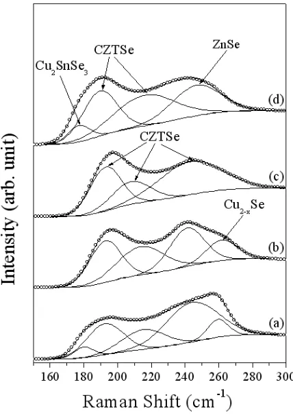
Figure 4 shows the Raman spectra and their evolution of the films versus the deposition potential. The main Raman shift peaks of CZTSe phase were identified at 190-194, 210-220 and 239-254 cm-1 according to the literature reports[10]. The Raman shift peaks at 260-263 cm-1 assigned to Cu2-xSe phase when the deposition potential were -0.9 and -1.0 V according to the literature[6]. It was
found that the Cu2-xSe phase formed at less negative potential as in Fig. 4. In addition, peak at 249 cm -1
might be assigned to ZnSe for the peak near 250 cm-1[15] when the deposition potential was -1.2 V. The Raman spectra of the films also indicated a peak assignable to Cu2SnSe3 at 180 cm-1[10] in Fig.
4(a) and (d). From above results, it indicates that the electrodeposition potential is a key function to alter the composition of the deposited CZTSe films. The films deposited at -1.1 V is better than other samples with no other secondary phase and good crystallinity.
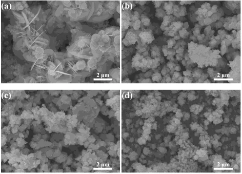
Figure 5 shows the SEM surface images of the films versus different deposition potential. It was found that the films were mainly composed of spherical nanoparticles. However, the films deposited at -0.9 V shows some plate-like particles with spherical nanoparticles as in Fig. 5 (a). The composition of the plate-like structure was examined from the energy dispersive X-ray analysis (EDX) to be only with Cu and Se. The plate-like particles are thus identified as Cu2-xSe and this is agreement
to the result of Raman spectra analysis.
[image:6.596.50.546.369.726.2]
Figure 6. The plots of (αhυ)2 against hυ of the CZTSe films versus the deposition potential: (a) V=-0.9, (b) V=-1.0, (c) V=-1.1, (d) V=-1.2.
The band gap of the films was determined from the optical absorption spectra. The relation between the absorption coefficient and the photo energy of band gap was expressed as the following equation [18]:
αhυ =A (hυ - Eg)n (1)
where α is the absorption coefficient, h is the Planck’s constant, υ is the frequency of the light, Eg is the optical band gap, A is the optical constant and n is a constant. The value of n is 1/2 for direct
transitions and 2 for indirect transitions. Figure 6 shows the plots of (αhυ)2 against hυ of the films as a function of deposition potential. The direct band gap was obtained by extrapolating the straight line part of the curves in this figure to the energy axis, where (αhυ)2 = 0. The direct band gaps of the films are found to be about from 1.22 to 1.36 eV and increase with decrease in Cu/(Zn+Sn) ratio. The films with higher Cu/(Zn+Sn) ratio are found to have higher optical band gap than the films with lower Cu/(Zn+Sn) ratio. It results from the lattice strain which was caused by the different Cu/(Zn+Sn) ratio of the thin films [8, 9].
4. SUMMARY
CZTSe films were obtained by potentionstatically deposition method. The electrodeposition potential cause the variations in the composition of the CZTSe films. The predominant phase of the films was found to be Cu2ZnSnSe4 from XRD and Raman analysis. Other minor phase of Cu2-xSe,
[image:7.596.156.437.68.328.2]
with some plate-like particles of Cu2-xSe phase. The direct band gaps of the films are found to be
about from 1.22 to 1.36 eV dependent of the composition variation. The film with lower Cu/(Zn+Sn) ratio in composition has higher direct band gap.
ACKNOWLEDGEMENT
Financial support of this research by Tatung University, Taipei, Taiwan, under the grant B101-T03-007 is gratefully acknowledged.
References
1. P. Jackson, D. Hariskos, E. Lotter, S. Paetel, R. Wuerz, R. Menner, W. Wischmann and M. Powalla, Prog. Photovolt: Res. Appl., 19 (2011) 894.
2. H. Katagiri, N. Sasaguchi, S. Hando, S. Hoshino, J. Ohashi and T. Yokota, Sol. Energy Mater. Sol. Cells, 49 (1997) 407.
3. M. P. Suryawanshi, G. L. Agawane, S. M. Bhosale, S. W. Shin, P. S. Patil, J. H. Kim and A. V. Moholkar, Mater. Technol., 28 (2013) 98.
4. K. Ito and T. Nakazawa, Jpn. J. Appl. Phys., 27 (1988) 2094. 5. W. Shockley and H. J. Quesser, J. Appl. Phys., 32(1961) 510.
6. P. M. P. Salomé, P. A. Fernandes and A. F. da Cunha, Thin Solid Films, 517 (2009) 2531-2534. 7. P. M. P. Salomé, P. A. Fernandes, A. F.da Cunha, J. PLeitão, J. Malaquias, A. Weber, J. C
González and M. I. N. da Silva, Sol. Energy Mater. Sol. Cells, 94 (2010) 2176-2180.
8. R. A. Wibowo, W. S. Kim, E. S. Lee, B. Munir and K. H. Kim, J. Phys. Chem. Solids, 68 (2007) 1908.
9. G. S. Babu, Y.B. K. Kumar, P. U. Bhaskar and S. R. Vanjari, Sol. Energy Mater. Sol. Cells, 64 (2010) 221.
10. M. Meng, L. Wan, P. Zou, S. Miao and J. Xu, Appl. Surf. Sci., 273 (2013) 613.
11. W. Septina, S. Ikeda, A. Kyoraiseki, T. Harada and M. Matsumura, Electrochim. Acta, 88 (2013) 436.
12. T. K. Todorov, J. Tang, S. Bag, O. Gunawan, T. Gokmen, Y. Zhu and D. B. Mitzi, Adv. Energy Mater., 3 (2013) 34.
13. G. M. Ilari, C. M. Fella, C. Ziegler, A. R. Uhl, Y. E. Romanyuk and A. N. Tiwari, Sol. Energy Mater. Sol. Cells, 104 (2012) 125.
14. S. Y. Zhang, C. Z. Fang, Y. P. Tian, K. R. Zhu, B. K. Jin, Y. H. Shen and J. X. Yang, Cryst. Growth Des., 6 (2006) 2809.
15. K. R. Murali, K. Thilakvathy, S. Vasantha and Rachel Ooomen, Chalcogenide Lett., 5 (2008) 111.
16. N. D. Boscher, C. J. Carmalt, R. G. Palgrave and I. P. Parkin, Thin Solid Films, 516 (2009) 4750. 17. Al-Mamun and A. B. M. O. Islam, Appl. Surface Sci., 238 (2004) 184.
18. A. Slav, Dig. J. Nanomater. Bios., 6 (2011) 915.