Compound Semiconductors
Gang LI
January, 1996
This thesis contains no material which has been
accepted for the award of any other degree or diploma
at any university and to the best of my knowledge and
belief, contains no material previously published or
written by another person except where due reference
is made in the text. The extent to which the thesis is
my own original work.
I am indebted to my supervisor, Dr. Chennupati Jagadish, for his guidance,
patience, enthusiasm and support.
I would like to thank my advisers, Prof. Jim Williams and Dr. Peter Kemeny, for
their invaluable support and encouragement. I also would like to thank Prof. Kui
Hong Yao for his support and encouragement.
There are a number of people in the department I would like to thank, in
particular, Dr. Nick Hauser for his assistance and discussions on
characterisation techniques and Mr. Andrew Clark for his discussion and
assistance with reactor maintenance and calibration.
Particular thanks are extended to Dr. Mladen Petravic for SIMS measurements
and Dr. Renate Egan, Dr. Andy Allerman, Mr. Hoe Tan, Dr. Rosa Leon, Dr.
Philip Hawker, Mr. Mike Aggett and Dr. Cory Larsen for their assistance and
discussions during the course. I would like to thank Ms. Toni Purdy for her
assistance with non-academic affairs.
I gratefully would like to acknowledge Prof. Mike Gal at The University of New
South Wales for optical characterisation and for granting me access to their
laboratory. I would like to thank Prof. Gal for his support and encouragement.
Many thanks to Dr. B.G. Svensson and Ms. M. Linnarsson at The Royal
Institute of Technology, Sweden, for SIMS measurements, Dr. Jarek
Antoszewski at The University of West Australia for variable-field Hall effect
Kidane Belay for proof-reading of part of this thesis.
I acknowledge financial support from The Australian International Development
Assistance Bureau (Equity and Merit Scholarship) and The Department of
Electronic Materials Engineering of The Australian National University (The
Australian National University Scholarship).
The major thrust of this work is on research and development of MOVPE growth techniques for producing high quality Si, Zn and C 8-doped layers in (Al)GaAs.
Si 8-doping is much more complicated in MOVPE than MBE as a result of higher growth temperatures and complicated gas phase chemistry. Due to the lack of a systematic study to date, Si 8-doping by MOVPE is not well understood. In this work, the growth of Si 8-doped (Al)GaAs is investigated in detail as a function of many growth parameters. Si 8-doped GaAs (A l^ G a ^ A s) layers with a peak electron density of 8 .5 x l0 18 (6 .8 x l0 18) cm '3 for an electron profile width of 58 (60)
A
have been achieved in the present work. Further results indicate that the electron confinement of Si 8-doped (Al)GaAs grown at normal MOVPE growth temperatures is controlled by thermal diffusion of the Si in the absence of segregation. The electron density is limited by the partial pressure of the Si doping species homogeneously generated in the gas phase. The Si 8-doping concentration is predominantly controlled by gas flow velocity, temperature, and SiH4 partial pressure.A detailed study of subband electronic structure of 2DEGs in Si 8-doped (Al)GaAs grown by MOVPE at a relatively high temperature of 700°C has also been carried out. The effect of cap layer structures on the symmetry of the V-shaped potential well is established and a weak and moderately persistent photoconductivity is also observed for the first time in Si 8-doped GaAs. At 1.5K, the illumination-generated electrons occupy an additional subband. This occupancy persists once the illumination has been turned off. The properties of DX centres in Si 8-doped (Al)GaAs is discussed as a function of A1 mole fraction.
and 1.64 eV for Zn 5-doped Al0 35Gao 65As. A model is proposed to quantitatively describe the Zn 8-doping concentration as a function of 5-doping parameters.
TMA1 is used as a C 5-doping precursor for the first time to grow C 8-doped (Al)GaAs layers with very high doping concentrations. The doping efficiency of TMA1 as a function of A1 mole fraction is investigated in detail, together with parameters influencing C 8-doping concentration and electrical activation of C atoms. Results show that electrical activation is mainly determined by self-compensation of the C atoms rather than H passivation but, using the optimised growth conditions, self-compensation can be eliminated. The best C 8-doped GaAs (A l^ G a ^ A s ) grown at 580°C has a peak hole density of 1 .4 x l0 19 (1 .6 x l0 19) cm'3 for a hole profile width of 88 (85) Ä. C 5-doped pipi
Contents
Chapter 1.
Introduction
1
Chapter 2.
MOVPE and characterisation techniques
7
2.1. MOVPE
7
2.2. Characterisation techniques
10
2.2.1. Conventional capacitance-voltage (C-V) measurements
10
2.2.2. Electrochemical capacitance-voltage (EC-V) measurements 13
2.2.3. Hall effect measurements
16
2.2.4. Magnetotransport measurements
19
2.2.5. Variable-field Hall effect measurements
22
2.2.6. Secondary ion mass spectroscopy (SIMS)
25
2.3. Summary
25
References
28
Chapter 3.
Si 5-doping
30
3.1. Introduction
30
3.2. Experimental details
32
3.3. Confinement of electrons in Si 5-doped (Al)GaAs
32
3.4. Parametric studies of electron density of Si 5-doped (Al)GaAs 37
3.4.1. Pre 5-doping parameters
37
3.4.2. 5-doping parameters
42
3.4.3. Post 5-doping parameters
49
3.5. Discussion
52
3.5.1. Generation of the Si doping species
52
3.5.2. Adsorption of the Si doping species
53
3.5.3. Desorption of the Si doping species
54
3.6. Conclusions
54
References
56
Chapter 4.
Subband electronic structure of Si 5-doped (Al)GaAs
58
4.1. Introduction
58
4.2. Experimental details
60
4.3. Subband electronic structure of Si 5-doped GaAs
60
4.3.1. Angular dependence of longitudinal magnetoresistance
versus tilted magnetic field trace
60
4.3.2. Subband electron density and mobility
65
4.3.3. Depopulation Shubnikov-de Haas oscillations (DSdHo)
69
4.4. Effect of illumination on subband electronic structure of
Si 5-doped (Al)GaAs
74
4.4.1. A weak and partially persistent photoconductivity in Si
4.4.2. Discussion on the occupancy of the DX centres
in Si 5-doped (Al)GaAs
82
4.5. Conclusions
88
References
89
Chapter 5.
Zn 5-doping
91
5.1. Introduction
91
5.2. Experimental details
93
5.3. New Zn 5-doping sequence
94
5.4. Parametric studies of Zn 5-doped (Al)GaAs
98
5.4.1. Variation of A1 mole fraction
98
5.4.2. Variation of 5-doping time
103
5.4.3. Variation of DMZn partial pressure
110
5.4.4. Variation of reactor pressure and carrier gas flow rate
113
5.4.5. Variation of 5-doping temperature
119
5.4.6. Hole mobility versus sheet hole density
123
5.5. Modelling of Zn 5-doping
123
5.6. Conclusions
131
References
132
Chapter 6.
C 5-doping
133
6.1. Introduction
133
6.2. Experimental details
136
6.3. The new C 5-doping precursor: TMA1
136
6.4. Parametric studies of C incorporation and electrical activation
of the C atoms in C 5-doped (Al)GaAs
141
6.4.1. Effect of A
sH3 addition to the gas phase
141
6.4.2. Variation of A1 mole fraction
144
6.4.3. Variation of TMGa and TMA1 moles
147
6.4.4. Variation of 5-doping temperature
150
6.5. Demonstration of C 5-doped pipi doping superlattices
in (Al)GaAs
153
6.5.1. Motivation
153
6.5.2. Growth conditions
154
6.5.3. Results and discussion
155
6.6. Conclusions
163
References
164
Chapter 7.
Summary
166
2 D E G (s ): 2 D H G (s ):
q u a s i-tw o d im e n s io n a l e le c tro n g as(s).
q u a s i-tw o d im e n s io n a l h o le gas(s).
fi: h: <Z>0:
P la n c k co n stan t/2 rc.
P la n c k c o n sta n t.
th e c h a n g e o f th e e x p e c ta tio n v a lu e o f th e g ro u n d -s ta te w a v e fu n c tio n u n d e r a p p lie d b ia s v o lta g e .
th e p e rio d o f S h u b n ik o v -d e H a a s o s c illa tio n s o f th e ith e le c tro n ic
su b b a n d in th e re c ip ro c a l m a g n e tic field.
A f l / B c o s Q ) : th e p e rio d o f S h u b n ik o v -d e H a a s o s c illa tio n s o f th e ith e le c tro n ic s u b b a n d in th e re c ip ro c a l m a g n e tic field . 0 is an a n g le b e tw e e n th e 8-
d o p e d p la n e n o rm a l a n d th e m a g n e tic fie ld d ire c tio n .
Az:
e:
r a:
sp a tia l w id th o f th e d o p a n t d istrib u tio n .
p e rm ittiv ity o f th e s e m ic o n d u c to r.
n o rm a lis e d Z n a d s o rp tio n ra te b y th e s u rfa c e d e n s ity o f th e
r d:
u n o c c u p ie d Z n a d s o rp tio n site s [ = 3 . 4 9 x l O 3 f p DMZn T ' 0'5]. n o rm a lis e d Z n d e s o rp tio n ra te by th e s u rfa c e d e n s ity o f th e o c c u p ie d
0 :
Z n a d s o rp tio n s ite s [ = 2 . 0 9 x 1 0 10 T e x p ( - ) ] .
an a n g le b e tw e e n th e 5 -d o p e d p la n e n o rm a l a n d th e m a g n e tic fie ld d ire c tio n .
k:
p.,(i= 0, 1 , .. .) :
a :
<70‘
Z :
2j q\
Z i ( i = 0 ,1
B o ltz m a n n c o n s ta n t.
H a ll m o b ility .
s u b b a n d c a rrie r m o b ility .
sta n d a rd d e v ia tio n o f G a u s s ia n d istrib u tio n .
d e p th -re s o lu tio n b ro a d e n in g .
d iffu s io n b ro a d e n in g .
e ffe c tiv e c o llis io n ra te o f Z n a to m s o n th e s u rfa c e
c o llis io n ra te o f Z n a to m s o n th e su rfa c e .
s p a tia l e x te n t o f th e w a v e fu n c tio n o f th e c a rrie rs in th e ith su b b a n d .
AsH 3: (A l)G a A s:
arsin e.
G a A s a n d A l^ G a ^ A s (x > 0).
B: * r
m a g n e tic field.
m a g n e tic fie ld in th e d ire c tio n p e rp e n d ic u la r to th e 2 D E G p la n e .
C -V : C V D :
c o n v e n tio n a l c a p a c ita n c e -v o lta g e , c h e m ic a l v a p o u r d e p o s itio n .
d: D :
D C X R D :
D L T S : D M Z n : D S d H o :
d o u b le c ry s ta l x -ra y d iffra c tio n ,
d e e p le v e l tra n s ie n t s p e c tro sc o p y , d im eth y lzin c.
d e p o p u la tio n S h u b n ik o v -d e H a a s o sc illa tio n s .
e:
E:
E a:
E d: E ;
e le m e n ta ry ch a rg e .
e le c tric fie ld fo rm e d in th e V -s h a p e d p o te n tia l w ell, a c tiv a tio n e n e rg y ,
d e s o rp tio n a c tiv a tio n e n e rg y .
e ig e n s ta te e n e rg y o f th e ith s u b b a n d in th e V -s h a p e d p o te n tia l w e ll
fo rm e d in 5 -d o p e d (A l)G a A s .
E C -V : e le c tro c h e m ic a l c a p a c ita n c e -v o lta g e .
/ :
If f t
-F:
E t o ta l’
EH i ''
EA sH 3 ’
ES iH 4 ' E t m a f
E D M Z n ’ E tM Go’
F E T s : F W H M :
F T IR :
s tic k in g c o e ffic ie n t o f Z n a to m s o n u n o c c u p ie d Z n a d s o rp tio n sites.
p e a k fre q u e n c y o f th e F F T p o w e r sp e c tru m , to ta l flo w ra te o f th e g ro u p I l l s in th e re a c to r,
to ta l flo w ra te in th e re a c to r. H 2 c a r r ie r g a s flo w rate ,
a rs in e flo w ra te , sila n e flo w rate ,
trim e th y la lu m in iu m flo w rate, d im e th y lz in c flo w rate ,
trim e th y lg a lliu m flo w rate, fie ld e ffe c t tra n sisto rs fu ll w id th a t h a lf m a x im u m .
F o u r ie r tra n s fo rm in fra re d sp e c tro s c o p y .
G a A s: G S M B E :
g a lliu m arsen id e .
g a s s o u rc e m o le c u la r b e a m e p ita x y .
H B T s : H E M T s :
h e te ro ju n c tio n b ip o la r tra n s isto rs h ig h e le c tro n m o b ility tra n sisto rs.
L E D s : lig h t e m ittin g d io d e s
m * : M :
M B E :
M O M B E : M O V P E :
M S an aly sis:
e ffe c tiv e m a ss o f c a rrie r, m o le c u la r w e ig h t,
m o le c u la r b e a m e p ita x y ,
m e ta l o rg a n ic m o le c u la r b e a m e p ita x y ,
m e ta l o rg a n ic v a p o u r p h a s e e p ita x y , m o b ility sp e c tru m an aly sis.
n 0:
n a ’
n s:
n T:
s u rfa c e d e n s ity o f th e Z n a d s o rp tio n site s (in C h a p te r 5 )
s u rfa c e d e n s ity o f th e o c c u p ie d Z n a d s o rp tio n sites,
* 3 +
n c v :
n H aU : n ( x ) :
t i i p i :
b u lk e le c tro n d e n sity .
e le c tro n d e n s ity o b ta in e d fro m th e C -V m e a s u re m e n t, e le c tro n d e n sity o b ta in e d fro m th e H a ll e ffe c t m e a su re m e n t, e le c tro n d is trib u tio n
p a n d n sta n d f o r p - ty p e a n d n -ty p e S -d o p e d la y e rs a n d i f o r u n d o p e d se p a ra tio n la y e rs, re s p e c tiv e ly .
n i p i is a stru c tu re c o n ta in in g a lte rn a tiv e ly n , i, p a n d i lay ers.
n i r t i : n s ta n d s f o r zi-type 8 -d o p e d la y e rs an d i f o r u n d o p e d s e p a ra tio n la y e rs,
re sp e c tiv e ly .
n i n i is a stru c tu re c o n ta in in g a lte rn a tiv e ly n a n d i lay ers.
n p e a k : p e a k e le c tro n d e n s ity .
P 2 d:
P a v e ' P \ s H 3 ’ P s i H 4 ' Pd m z h:
Pe c v: PhoII' p i p i :
s h e e t h o le d e n sity .
a v e ra g e h o le d e n s ity o f C 5 -d o p e d p i p i d o p in g su p e rla ttic e .
p a rtia l p re s s u re o f a rsin e .
p a rtia l p re s s u re o f sila n e. p a rtia l p re s s u re o f d im e th y lz in c .
s h e e t h o le d e n s ity o b ta in e d b y in te g ra tin g h o le p ro file .
s h e e t h o le d e n s ity o b ta in e d u s in g th e H a ll e ffe c t m e a su re m e n t.
p s ta n d s f o r p - ty p e 8 -d o p e d la y e rs a n d i f o r u n d o p e d s e p a ra tio n la y e rs, re s p e c tiv e ly .
p i p i is a s tru c tu re c o n ta in in g a lte rn a tiv e ly p a n d i lay ers. p p m :
P P’ re a c to r’
p a rts p e r m illio n , r e a c to r p re s s u re .
Q W (s): q u a n tu m w e ll(s).
r R T D s:
R x x :
g ro w th ra te o f (A l)G a A s e p ita x ia l la y er, re s o n a n t tu n n e llin g d io d e s,
lo n g itu d in a l m a g n e to re s is ta n c e
s.l.m .:
seem : S d H o : S iH 4:
S IM S :
g a s flo w ra te u n it (s ta n d a rd litre p e r m in u te ) g a s flo w ra te u n it (s ta n d a rd c m 3 p e r m in u te )
S h u b n ik o v -d e H a a s o sc illa tio n s,
silane.
s e c o n d a ry io n m a s s sp e c tro sc o p y .
t:
h :
S p u rg e’ tp o s t' tp r e ’ T , T 8:
TM A 1:
T M A s: T M G a :
p o s t-a n n e a lin g tim e.
8 -d o p in g tim e.
p u rg e tim e (in c lu d in g b o th p re a n d p o s t p u rg e )
p o s t p u rg e tim e ,
p re p u rg e tim e .
8 -d o p in g te m p e ra tu re ,
trim e th y la lu m in iu m . trim e th y la rse n ic .
U H P : ultra high purity. v:
V /III ratio :
y f
gas flo w v elo city in the reactor.
m ole ra tio o f the group V and the group III sp ecies in the gas phase, vibration frequency
x:
X o '
xv:
A1 m ole fraction o f A lG aA s.
Miniaturisation of spatial dimensions of semiconductor structures and devices is motivated by increased speed, reduced power consumption, and higher functional density of active devices and integrated circuits. It is a vital part of present and future semiconductor technology to advance materials science research in order to reduce spatial dimensions and at the same time to realise and understand physical mechanisms that impose fundamental limits on further scaling-down. 8-doping (also called atomic layer doping) is a novel doping technique which spatially confines the dopants to one or a few monolayers of the host semiconductor lattice. The realisation of 8-doped semiconductors represents a fundamental limit on the doping technique.
In ideal Si 8-doped GaAs, Si atoms are spatially confined in one atomic layer (which is considered as a 8-doped plane). The dopant profile can be described by Dirac's 8- function. The ionised Si donors create a continuous sheet of positive charges, which consequently bends the conduction band to form a V-shaped potential well. Due to electrostatic attraction, the electrons remain close to their parent ionised donors. When the doping concentration is high enough that the geometrical dimension of the V-shaped potential well is comparable to the de Broglie wave length of free electrons, the electron energies for motion perpendicular to a 8-doped plane will be quantised. The electrons confined in the Si 8-doped layer can therefore be considered as a quasi-two dimensional electron gas (2DEG). Similarly, a quasi-two dimensional hole gas (2DHG) can be formed in C or Zn 8-doped GaAs.
Theoretical calculation shows that the subband electronic structure of a 2DEG in Si 8- doped GaAs relies on free electron density and spatial confinement of the Si atoms. When the width of the Si atom profile is less than the spatial extent of the ground-state wavefunction o f the electrons, a further reduction of the spatial confinement of the Si atoms does not significantly change subband electronic structures [Schubert et al. 1986, Zrenner et al. 1985]. Indeed, a 8-doped semiconductor is defined as a structure that "contains a one-dimensional doping profile whose distribution width is smaller than
the spatial extent o f the ground-state wavefunction o f the free carriers ". [Koch et al.
1989, Schubert 1990].
2DEGs and 2DHGs formed in 8-doped (Al)GaAs have three distinct features from those realised in AlGaAs/GaAs based heterojunctions or quantum wells (QWs). (1) Even at moderate 8-doping concentration, the carriers already populate several excited subbands,
subbands are occupied in Si 5-doped GaAs [Schubert et al. 1986]. (2) The carriers populating the ground-state subband exhibit the lowest mobility in comparison to the excited subbands due to the proximity of the bare ionised impurities. (3) The electronic wave-function is considerably delocalised in the direction normal to the 5-doped plane. In addition to these unique electronic properties, spatial confinement of free carriers in 8- doped (Al)GaAs has attracted considerable interest not only for fundamental studies [van de Stadt et al. 1995, Wilks et al. 1994] but also for applications to novel devices, such as HEMTs [Harris et al. 1993, Kim et al. 1993, Passenberg et al. 1993, Pfeiffer et al. 1989, ], FETs [Jeong et al. 1992], HBTs [Goossen et al. 1991], LEDs [Hasnain et al. 1986, Schubert et al. 1985], lasers [Schubert et al. 1989], photodetectors [Tempel et al. 1990, Vanhatalo 1992], modulators [Larsson et al. 1991,1992], 5-doped nini and pipi doping superlattices [Ploog et al. 1988, Sasa et al. 1985], non-alloyed ohmic contacts [Marcy et al. 1991, Geraldo et al. 1993], band offset tuning [Scandolo et al. 1993], and RTDs [Houng et al. 1992, Wang et al. 1990].
8-doped layers were first grown by Wood et al. [1980] using MBE to synthesise complex free carrier profiles in GaAs. To date, 8-doping in different host materials such as GaAs, AlGaAs, Si [Eisele 1989, Nikiforov et al. 1991], InP [Cheng et al. 1989, Forte- Poisson et al. 1989, Ishikawa et al. 1991] with different dopants such as Si, C, Zn, Be, Sb [Eisele et al. 1989], and B [Powell et al. 1991] has been implemented using a variety of growth techniques including MBE, MOMBE, MOVPE, chloride CVD [Imaizumi et al. 1991]. The conventional growth sequence of a 5-layer in a semiconductor (called a 5- doping sequence) is composed o f a pre-5-doping purge step after growth of an undoped buffer layer, a 8-doping step with introduction of a doping species, and a post-5-doping purge step followed by growth of an undoped cap layer. During purge steps and the 5- doping step, growth o f the host material is completely suspended by venting the growth species, such as trimethylgallium (TMGa) and trimethylaluminium (TMA1) in MOVPE. In the last decade, MBE-grown 5-doped (Al)GaAs has been extensively studied and relevant work has been recently reviewed [Harris 1993a, Schubert 1993, Schubert 1994]. Although MOVPE is one o f the most widely used growth techniques for (Al)GaAs, growth of 5-doped (Al)GaAs by MOVPE has not been systematically studied or well understood. Particularly with p-type 8-doping, MOVPE has achieved much less success than MBE [Hobson et al. 1989, Schubert et al. 1990a].
composition and bulk-doping concentration are briefly described in Chapter 2.. Characterisation techniques, which are frequently used in this work, along with brief description of facilities, are also given in Chapter 2. Some results obtained using these characterisation techniques are presented for the purpose of demonstration.
Silicon (Si) 8-doped (Al)GaAs grown by MOVPE has been previously reported. However, the lack of any comprehensive study prevents from a detailed understanding of the Si 8-doping mechanism and applications of Si 8-doped structures. In Chapter 3, a number of growth parameters are systematically varied to investigate their effects on electron confinement and electron density in Si 8-doped (Al)GaAs. The Si diffusion coefficients are estimated using electron profiles of as-grown Si 8-doped (Al)GaAs. The Si 8-doping mechanism and the key factors which dominate Si 8-doping are therefore discussed on the basis of experimental results.
In Chapter 4, magnetotransport measurements in tilted magnetic fields and variable-field
Hall effect measurements are combined to characterise the subband electronic structure o f Si 8-doped (Al)GaAs with assistance of fast Fourier transform analysis and mobility spectrum analysis. This is the first systematic report on experimental results of subband electronic structure of 2DEG in Si 8-doped (Al)GaAs grown at 700°C by MOVPE. The effect of various cap layers on subband electronic structure is observed. Electronic properties of 2DEG is further studied by means of illuminating Si 8-doped (Al)GaAs at 1.5K. A weak and moderately persistent photoconductivity is observed and its effect on subband electronic structure is experimentally investigated. The relevant discussion provides new insight into the status of DX centres in Si 8-doped (Al)GaAs.
Carbon (C) has been considered as an ideal p-type dopant in (Al)GaAs due to its unique
properties. In
Chapter 6
, TMA1 is used for the first time as a C 5-doping precursor in
MOVPE. Very high C 5-doping efficiency, independent of A1 mole fraction, is observed
and discussed. A major effort is then placed on a parametric study of C 5-doping
concentration and electrical activation of the C atoms in C 5-doped (Al)GaAs. Self
compensation rather than H passivation is considered as the major cause for the C atom
electrical activation less than unity. C 5-doped (Al)GaAs is also used to fabricate
pipi
doping superlattices and C bulk-doped-like layers in (Al)GaAs, having a very high hole
density, are successfully demonstrated. C 5-doped
pipi
doping superlattices constitute a
promising alternative to the other C bulk-doping approaches.
Finally,
Chapter 7
provides a summary of the key results of this thesis.
References
Cheng W., Zrenner A., Ye Q.Y., Koch F., Grutzmacher D. and Balk P., (1989)
Semicond. Sei. Technol., 4, 16.
Eisele L, (1989) Appl. Surf. Sei., 36, 39.
Forte-Poisson M.A., Brylinski C. and Blondeau E., (1989) J. Appl. Phys., 66, 867.
Geraldo J.M., Rodrigues W.N., Medeiros-Ribeiro G. and de Oliveira A.G., (1993) J.
Appl. Phys., 73, 820.
Goossen K.W., Cunningham J.E., Kuo T.Y., Jan W.Y. and Fonstad C.G., (1991) Appl.
Phys. Lett., 59, 682.
Hasnain G., Dohler G.H., Whimery J.R., Miller J.N. and Dienes A., (1986) Appl. Phys.
Lett., 49, 1357.
Harris J.J., Murray R. and Foxon C.T., (1993) Semicond. Sei. Technol. 8, 31.
Harris J.J., (1993a) J. Mater. Sei., Mater, in Electronics, 4, 93.
Hobson W.S., Pearton S.J., and Schubert E.F., (1989) Appl. Phys. Lett., 55, 1546.
Houng M.P., Wang Y.H., Chen H.H. and Wei H.C., (1992) J. Appl. Phys., 71, 780.
Imaizumi T., Seiwa M. and Oda O., (1991) J. Crystal Growth 115, 443.
Ishikawa H., Miwa S., Maruyama T. and Kamada M., (1991) Appl. Phys. Lett.,
58, 851.
Jeong D.H., Jang K.S., Lee J.S. and Jeong Y.H., (1992) IEEE Electron Dev. Lett., 13,
270.
Kim Y., Kim M.S. and Min S.K., (1993) Appl. Phys. Lett., 62, 741.
Koch F. and Zrenner A., (1989) Mater. Sei. and Eng. Bl, 221.
70,514.
Nikiforov A.I., Kanter B.Z., Stenin S.I. and Rubanov S.V., (1991) Mater. Sei. Forum
69, 17.
Passenberg W., Bach H.G., Böttcher J. and Kunzel H., (1993) J. Crystal Growth 127,
716.
Ploog K, Hauser N. and Fisher A., (1988) Appl. Phys., A45, 233.
Powell A.R., Mattey N.L., Kubiak R.A.A., Parker E.H.C., Whall T.E. and Bowen D.K.,
(1991) Semicon. Sei. & Technol., 6, 227.
Sasa S., Saito J., Nanbu K., Ishikawa T, Hiyamizu S. and Inoue M., (1985). Jpn. J. Appl.
Phys., 24, L281.
Scandolo S. and Baldereschi A., (1993) Proceedings of International Symposium
Physical Concenpts and Materials for Novel Optoelectronic Device
Application II. (eds) F. Beltram and E. Gomik, SPI, Vol. 1985, p.143.
Schubert E.F., Fischer A., Horikoshi Y. and Ploog K., (1985) Appl. Phys. Lett., 47, 219.
Schubert E.F., Fischer A. and Ploog K., (1986) IEEE Trans. Electron Dev.,
ED-33, 625.
Schubert E.F., van der Ziel J.P., Cunningham J.E. and Harris T.D., (1989) Appl. Phys.
Lett., 55, 757.
Schubert E.F., (1990) Mater. Sei. Forum, 65-66, 53.
Schubert E.F., Kuo J.M., Kopf R.F., Luftman H.S., Hopkins L.C., and Sauer N.J.,
(1990a), J. Appl. Phys., 67, 1969.
Schubert E.F., (1993), in " Doping in III-V semiconductors " Published by the Press
Syndicate of the University of Cambridge.
Schubert E.F., (1994) in " Semiconductors and Semimetals " Vol. 40, (ed.) A.C.
Gossard, Acdemic Press, p.l.
Tempel G., Muller F., Schwarz N., Koch F., Werimann G., Zeindl H.P. and Eisele I.,
(1990) Surf. Sei., 228, 247.
van de Stadt A.F.W., Bogaerts R., Koenraad P.M., Leopold H., Herlach F., and Wolter
J.H., (1995) Physics B211, 458.
Vanhatalo J., (1992) III-Vs Review, 5, 32.
Wilks S.P., Cornish A.E., Elliott M., Woolf D.A., Westwood D.I., and Williams R.H.,
(1994), J. Appl. Phys., 76, 3583.
Wang R.L., Su Y.K., Wang Y.H. and Yam K.F., (1990) IEEE Electron Dev. Lett., 11,
428.
2.1. MOVPE
Metal organic vapour phase epitaxy (MOVPE) is a cold wall chemical vapour phase deposition process. The general embodiment utilises reactions of metal alkyl, such as trimethylgallium (TMGa), trimethylaluminium (TMA1), with hydrides of the non-metal species,
i.e.
arsine (AsH3). The most common reactions for growth of (Al)GaAs areGa(CH3)3 + AsH 3 ==> GaAs + 3CH4
xA1(CH3)3 + ( 1-x) Ga(CH3)3 + AsH3 ===> AlxGaj.xAs + 3CH4
The growth ambient in the MOVPE reactor is a carefully controlled mixture of metal organic precursors and hydrides in the ultra-high purity (UHP) H2 carrier gas. Theory and practice related to MOVPE have been comprehensively described in good books [Stringfellow 1989, Razeghi 1989, 1995].
In this work, a modified MR Semicon MOVPE reactor is used to grow S-doped (Al)GaAs structures. The reactor is schematically shown in
Fig. 2.1.,
which has two TMGa sources and two TMA1 sources. Two metal organic sources enable TMGa or TMA1 flow rate to be varied from one step to the other without ramping. The change of 100% AsH 3 flow rate also benefits from availability o f two AsH3 lines separately controlled by mass flow controllers. 500 ppm silane (SiH4) and 5000 ppm dimethylzinc (DMZn), both diluted in UHP H2, are used as zi-type and p-type doping precursor, respectively. The reactor pressure is normally operated at 76 Torr with UHP H2 as a carrier gas.Arsine Silane DMZn
To Scrubber IR heating lamps
Hydrogen
Gas-mixer TMGal TMGa2 TMAI1 TMAI2 Wafer
Vent/Run gas switching manifold
was found that the uniformity is almost independent of growth temperatures (600°C - 750°C) and the total flow rate of metal organic (group III) precursors (or growth rate) but dramatically affected by H2 carrier gas flow rate or reactor pressure. The carrier gas flow rate was varied from 2 s.l.m. to 20 s.l.m. at a fixed reactor pressure of 76 Torr to find the best layer thickness uniformity. Using a carrier gas flow rate of 17.5 s.l.m., the thickness variation across 2" wafer is less than 2%. The growth rate calibrated as a function o f the total flow rate (in moles/min) of the group
in
precursors is given by r = 167( 1135.3112F +0.0029557 ) (2.1.)where r is growth rate (Ä/s) and F is the total flow rate of group III precursors (moles/min).
Composition:
Composition o f AlGaAs is correlated with composition of vapour phase. The latter is determined by the ratio of TMGa and TMA1 flow rates. Under different vapour phase compositions, A1 mole fraction of epitaxial AlGaAs layers is characterised using double crystal x-ray diffraction (DCXRD), low temperature photoluminescence and photoreflectance. The A1 mole fraction of AlGaAs as a function of TMGa and TMA1 flow rates can be expressed asX = 0.024 + 0.548x , + 0.4279x 2, 2
x . = FtMAI I ( FtMAI + ^TMCa )
where x and x y are A1 mole fraction in AlGaAs and in the gas phase, respectively, F TMGa and F TMAl are the flow rates of TM Ga and TMA1 (moles/min), respectively. It was found that the change o f growth temperature or growth rate over the experimental range does not affect validation o f Eq. 2.2..
n-type
and
p-ty p edoping of (Al)GaAs:
/i-type and p-type doping of (Al)GaAs are realised introducing SiH4 and DMZn into the gas phase along with group III and V precursors, respectively. The Si doping concentration increases with increasing SiH4 partial pressure or temperature but decreases with increasing H2 carrier gas flow rate or growth rate. The Zn doping concentration increases with increasing growth rate or DMZn partial pressure. A reduced temperature leads to a significant increase o f Zn bulk doping concentration. The effect of A1 mole fraction on Si and Zn bulk-doping concentration is negligible. Two empirical equations describing electron density as a function o f SiH4 flow rate at a TMGa flow rate of 3 .3 5 x l0 '5 moles/min and TM Ga flow rate at a SiH4 flow rate of 10'8 mole/min are given as follows.log(n3d ) = 1.0226 log[FSiH ]
+24.7588
21 ‘ 16
n3d
=-1.53892
x1021 [FTMGa ] + 8.9428
x1016
where
n3J
is Si bulk-doping concentration (cm'3), andFSiH4
andFTMGa
are the flow rates of SiH4 and TMGa (moles/min). The other parameters were fixed at temperature: 750°C, H2 carrier gas flow rate: 17.5 s.l.m., and cell pressure: 76 Torr.2.2. Characterisation techniques
A number o f techniques are frequently used to characterise 8-doped (Al)GaAs. Basic principles, brief description o f facilities and some consideration on how to perform appropriate measurements are presented in this
Section.
In addition, some typical results obtained in this work are also demonstrated. The detailed data analysis will be given in the comingChapters.
2.2.1. Conventional capacitance-voltage (C-V) measurements
Capacitance-voltage (C-V) profiling is a powerful technique to spatially resolve carrier distribution in semiconductors. The detailed theory and procedure of C-V measurements have been described in standard textbooks
[e.g.
Bloodet al.
1992].non-potential well tilted by applied negative bias voltage. The depth resolution of C-V profiling is determined by the spatial extent of the ground-state wavefunction [Schubert et al. 1988, 1989].
The spatial extent of the ground-state wavefunction in an ideal 8-doped semiconductor can be calculated using the equations[Schubert et al. 1989]
where z0: the spatial extent of the unperturbed ground-state wavefunction,
n2d
: the sheet carrier density, <z>0: the change of the expectation value of the ground-state wavefunction. A further self-consistent calculation shows that the width and peak carrier concentration of C-V profiles sensitively depend on spatial distribution of the dopants at a fixed sheet carrier density [Schubert et al. 1989]. For example, in Si 8-doped GaAs with a sheet electron density of 7 .5 x l0 12 cm'2, the width and peak electron density of the C-V profile are 41±4Ä and 1 .3 2 x l0 19cm'3 for Az = 2 Ä, and 95±5 Ä and 8 .5 x l0 18 cm'3 for Az = 50Ä (where Az is the proposed spatial width of the dopant distribution). Hence, C-V measurement is well suited to spatially resolve carrier profiles of as-grown or ex-situ post- annealed 8-doped (Al)GaAs. The width of C-V profiles can be used to carry out a study o f thermal diffusion and surface segregation of the dopants in 8-doped (Al)GaAs [Cunningham et al. 1991, Schubert et al. 1988a]. More importantly, although the C-V profile has no immediate physical meaning in 8-doped (Al)GaAs, the integration of a C-V profile represents the sheet carrier density [Schubert et al. 1988b, 1989] and the centroid of the C-V profile coincides to the peak position of the true carrier distribution [Kroemer et al. 1980, Schubert et al. 1989].In the present work, C-V measurements were carried out with Hewlett Packard 4280A 1 MHz C meter/C-V plotter controlled by computer. The experimental set-up is schematically shown in Fig. 2.2.. Circular Schottky contacts with a diameter of 0.6 - 1
(2.4.)
Sample Holder
Personal Computer
Temperature Controller
Co-processor Card
HP Measurement
HP 4280A 1MHZ C Meter/C-V Plotter
[image:25.552.69.509.55.798.2](Al)GaAs, respectively. Chemical cleaning was employed before evaporation in order to improve the quality o f the Schottky diodes. The C-V measurement temperature can be varied between 360K to 77K. A red LED mounted in the sample box allows a study of illumination effect on C-V profiles. A typical C-V profile of Si 8-doped GaAs is demonstrated in Fig. 2.3., which illustrates a peak electron density of 8 .5 x l0 18 cm'3 with a electron profile width (full width at half maximum) of 6 nm.
2.2.2. Electrochemical capacitance-voltage (EC-V) measurements
Profiling depth of C-V measurement is limited by breakdown voltage of a Schottky diode, particularly in the case where the 8-doped layer has very high doping concentration. Obviously, multiple 8-doped (Al)GaAs can not be profiled by C-V measurement. EC-V uses the same principle as C-V but the former substitutes stepped surface etching for stepped reverse bias voltage. Very small bias voltage applied during EC-V measurement avoids the problem with breakdown o f the Schottky diode. Using the step-by-step etching process, a very large depth can be profiled, such as multiple 8-doped (Al)GaAs (see Fig.
2.4.). Detailed theory and practice of EC-V measurements can be found in textbooks [e.g.
Blood et al. 1992].
In this work, EC-V measurements were carried out with a BIO-RAD PN 4300 profiler using NaOH:EDTA as an electrochemical etching solution. The depth of each stepped surface etching can be varied from 10 Ä to thousands of
A.
Once one uses the smallest etching depth, the etching process should not influence the carrier profile since the spatial extent o f the ground-state wavefunction estimated by Eqs. 2.4. and 2.5. is already larger than this etching depth. The problems with EC-V profiling of 8-doped (Al)GaAs is how to avoid unusual folding back o f the profile, a change in carrier type, and effect of roughness of the etching front surface. A number of measurement parameters, such as model, frequency, bias voltage, and sealing ring size [BIO-Rad PN 4300 Manual], have been varied to optimise measurement conditions. In some cases where the peak carrier concentration of 8-doped layers was extremely high (for example, > 1 - 5 x l0 19 cm'3), the cap and buffer layers were intentionally slightly doped to a carrier concentration of ~ 5 x l0 17 cm '3 in order to ensure the quality of EC-V profiles.Depth (Ä)
Si 5-doped GaAs
[image:27.552.109.480.64.565.2]Hole
D
e
n
s
ity
(cm
3
)
Zn 6-doped AI0 35Ga0 65As
Zn 5-doped GaAs
0.0
0.4
0.8
1.2
Depth (pm)
[image:28.552.92.508.64.557.2]high hole densities with very narrow hole profile widths are obtained in GaAs and
AI
q35Ga065
A
sboth grown in MOVPE using the new Zn 8-doping sequence developed in this work. An A1 mole fraction dependence of the hole confinement and hole density in Zn 5-doped AlGaAs can also be found in Fig. 2.4.. A more detailed study will be presented in Chapter 5.2.2.3. Hall effect measurements
The Hall effect has been widely used to characterise semiconductors. Free carrier type, density and mobility can be obtained from Hall effect and conductivity measurements. Detailed analysis of the Hall effect data over a wide temperature region can give more information concerning impurities, imperfections, uniformity, scattering mechanism, etc., which is not available from any other single technique [Blood et al. 1992].
The Hall effect measurements are also used to perform studies of 5-doping concentration in (Al)GaAs as a function of growth parameters [Kikkawa et al. 1991, Koenraad et al. 1990, Sakaguchi et al. 1992, Tromby et al. 1994]. The principle and procedures are similarly straightforward. However, two complications should be borne in mind. One is the existence of quantum Hall effect where the Hall resistance at high magnetic fields is no longer a linear function o f magnetic field but shows a series of plateau. The Hall effect measurement needs to be done in the low magnetic fields so that p B z < 1 (where B z is the magnetic field and fi is the mobility). This condition can be easily met in 5-doped (Al)GaAs since the mobility of quasi-two dimensional electron or hole gases (2DEGs, 2DHGs) formed in these structures is very low. The other complication is parallel conductance resulting from multiple subband occupancy in 8-doped (Al)GaAs. The effect o f parallel conduction on the Hall effect measurement can be briefly discussed using a simple case where two parallel conductive channels (i = 1 and 2) exist in the system. The sheet carrier density (n2d) and mobility (ji) obtained from the Hall effect measurement under low magnetic fields ( jiß z « 1) are determined by [Kane et al. 1985]
( n i\^i n2^2)
( HjHi + n2^-2 )
( n , \ i , + n 2n 2 ) (2.7.)
1990, 1990a, Schubert et al. 1987].
Si 8-doped GaAs with different doping concentrations were characterised using the C-V and Hall effect measurements.
Table 2.1.
illustrates that both the techniques give similar results on the sheet electron density when the 8-doping concentration is low enough that few subbands are occupied. Even at high doping concentrations, the difference in the electron density obtained using different techniques is small and within experimental error. A similar comparison was previously reported by Tromby et al. [1994].In this work, the Hall effect measurements were carried out at low magnetic fields (< 2 T) over the temperature range of 1.5K to 300K. The system is schematically shown in
Fig.
2.5.. The measurement procedure follows the Keithley manual [1985] and the van der Pauw geometry was employed. Au(88wt%)-Ge(12wt%) for Si 8-doped and Au(95wt%)- Zn(5wt%) for Zn and C 8-doped (Al)GaAs were thermally evaporated through a shadow mask and alloyed at 430°C for 30 - 35s to form ohmic contacts with a diameter of 0.8 mm. The contacts were placed at the comers of square samples, 6 mm x 6 mm in size. The resistance ratio was within 1 ±0.005.
Table 2.1. Comparison o f sheet electron density obtained using C-V and
Hall effect measurements at room temperature
Samples Mobility (cm2/sV) Sheet electron density (cm'2)
Hall C-V
MR510 2723 3-OxlO12 2 .9 x l0 12
MR511 3127 2 .4 x l0 12 2 .4 x l0 12
MR512 2651 4 .2 x l0 12 4 .8 x l0 12
IEEE 488 Interface
Computer
Current Source
M P6186C
Sample
Keithley 181
Nano-voltmeter
Switch Box
[image:31.552.57.511.57.499.2]Shubnikov-de Hass oscillations (SdHo) are essentially a quantum mechanical phenomenon which occurs when the conduction (or valance) band states are magnetically quantised. The basic principle for SdHo is that, as the magnetic field perpendicular to a 2DEG plane is increased, the Landau levels associated with each subband sweep through the Fermi level, causing a change in the density of states at the Fermi level which manifests itself as a series of oscillations in the longitudinal magnetoresistance, Rxx. Each subband induces a set of oscillations periodic in 1/BZ as expressed below if spin splitting is neglected
n i = h A : ( l I B ) (2.8.)
where, n,. is the subband electron density, Bz is the magnetic field perpendicular to the 2DEG plane, and the At{ l / B z) is the period of the SdHo of the ith electronic subband in the reciprocal magnetic field. In 5-doped (Al)GaAs, more than one subband are normally occupied and the electron density significantly differs from one subband to the other. Each subband generates a set of SdHo with a period determined by its electron density. As a result, the Rxx versus B z curve is a convolution of multiple SdHo with different periods. A typical R xx versus Bz curve obtained from Si 5-doped GaAs is illustrated in
Fig. 2.6.. In order to derive subband electron densities, fast Fourier transform (FFT) analysis has to be applied to analyse this Rxx versus Bz curve. The FFT analysis involves (1) the derivative dRxJ d B z is calculated digitally; (2) the FFT power spectrum for Rxx is derived from FFT analysis of dRxJ d B z versus 1IBV and (3) the peak frequencies of the FFT power spectrum are then converted into sheet electron density using the equation
n{ = 2 x 2 . 4 x 10¹⁰ x f FFT (2.9.)
where ni is the sheet electron density of the ith occupied subband and f FFT is the peak frequency o f the FFT spectrum. A FFT spectrum whose frequency has been converted into the sheet electron density is illustrated in Fig. 2.7.. From the FFT spectrum, the subband electron densities of Si 5-doped GaAs can be easily obtained. More discussion on determination o f subband electron densities o f Si 5-doped (Al)GaAs will be given in
a
c
as
w ' ( / )
CD
k _ O a?
c
CD CD
Magnetic Field (T)
Fig. 2.6. The longitudinal magnetoresistance (Rxx) as a function of magnetic field
F
F
T
I
n
te
n
si
ty
(
a
rb
.
u
n
it
)
2x10 12
4 x10¹²
6x10¹²
8x10¹²
Electron Density (cm 2)
Fig. 2.7. The FFT spectrum derived from the
Rxx
versusBz
curve shown inFig.
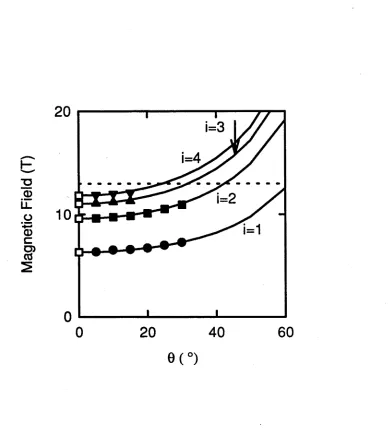
When the magnetic field is applied parallel to a 2DEG plane, very weak SdHo results only from bulk electrons. If a strong enough magnetic field is applied parallel to a Si 8- doped layer in (Al)GaAs, however, the longitudinal magnetoresistance,
Rxx,
oscillates in a manner analogous to the SdHo effect (seeFig. 2.8.).
These strong oscillations are designated as depopulation SdHo (DSdHo). The origin has been discussed previously in terms of depopulation of the electrons from the top-most occupied subband and redistribution in the lower subbands [Ando et al. 1982, Newson et al. 1986]. In combination with the FFT analysis of theRxx
versusBz
curve in which the magnetic field is applied perpendicularly to the Si 8-doped layer, the DSdHo will be complementarily used to reveal the subband electronic structures, particularly with a study of occupancy of the top-most subbands under different conditions.M agnetotransport measurements were carried out with an Oxford Cryostat (High Field Spectromag 2000) operated under magnetic fields (0 - 13 T) at the temperature of 1.5K (see
Fig. 2.9.).
The cryostat incorporates Lakeshore 612 Magnet Power Supply, Oxford Temperature Controller ITC503, Keithley 485 Autoranging Picoammeter, Keithley 7001 Switching System, Keithley 196 System DMM, and Keithley 220 Programmable Current Source. The system was controlled by home-programmed HP-BASIC software. The sample holder is rotatable so that the angle of the magnetic field direction with respect to a 5-doped layer normal can be changed from 0° to 90°. A red LED mounted on the sample holder allows to illuminate the sample after it has been cooled down in the dark. The light intensity was adjusted by the applied current to the LED. The sample geometry and ohmic contact preparation were described inSection 2.2.3..
2.2.5. Variable-field Hall effect measurement
Well-known Hall effect measurements at a single magnetic field provides limited information about electronic subband structures of 5-doped (Al)GaAs (see
Section
2.2.3.).
The magnetotransport measurement can provide more detailed information but the measurements must be carried out at very low temperatures (< 50 K) and very high magnetic fields. The variable-field Hall effect measurements developed recently allow to derive subband electron density as well as mobility of Si 8-doped (Al)GaAs at high temperatures [Brugger et al. 1995, Beck et al. 1987, Koenraad et al. 1992, Panaev et al.1993].
10
12
Magnetic Field B (T)
Fig. 2.8. The DSdHo of Si 5-doped GaAs grown at 700°C. Measurement
Computer
Keithley
Switch 7001
Keithley 196 DMM Keithley 485
Picoammeter
Keithley 220
Current Source
Temperature
Controller Lakeshore
Magnet Power Supply
Oxford High Field Spectromag 2000 Sample Holder
2.2.4..
The Hall data (resistivity and Hall coefficient) were recorded at typically 10 to 15 different magnetic fields between 0.005T to 2T. The magnetic fields and applied currents were automatically reversed to eliminate voltage offsets and spurious voltage. The subband electron density and mobility were extracted using mobility spectrum (MS) analysis of the magnetic field dependent Hall data. Some consideration on variable-field Hall effect measurement of Si 8-doped GaAs has been discussed previously [Panaev et al. 1993]. A typical mobility spectrum which gives subband electron densities and mobilities o f Si 5-doped GaAs is illustrated inFig. 2.10..
The sample geometry and ohmic contact preparation were described inSection 22.3..
2.2.6. Secondary ion mass spectroscopy (SIMS)
SIMS is a structural method to profile dopant distribution with depth. The application of SIMS to 8-doped semiconductors has been discussed previously [Dowsett el al. 1992, Vandervorst et al. 1992]. In this work, SIMS measurements were performed with a Riber MIQ 256 quadruple-type secondary ion mass spectrometer and/or Cameca IMS-4F secondary ion mass spectrometer. A 3.5 - 9 keV primary Cs+ beam at 45° angle of incidence with respect to surface normal was employed. The best dynamic range for Zn was obtained by collecting (133Cs64Zn)+ ions. Ion-implanted samples were used as a reference to convert SIMS signal intensity to atomic density in units of cm'3. The depth scale was calibrated measuring sputtered crater depth. The measured depths agree within ±10% with the depth o f S-doped layers based on growth rate calibration.
A typical Zn atom profile o f multiple Zn 8-doped Al035Ga065As is illustrated in
Fig.
2.11..
Although the Zn atom profile is a little broader than the corresponding hole profile, the depth resolution does not significantly degrade with increasing sputtering depth. With a comparison between SIMS and C-V or EC-V profiles, the electrical activation of the dopants incorporated through 8-doping can also be estimated. More detailed studies are given inChapters 5
and6.
2.3. Summary
1 0 19
E
1018
" 1 0 17 ®
Q
E
I
1016
c
INI
1 0 15
0
500
1000
1500
Depth (nm)
Fig. 2.11. A Zn atom profile obtained using SIMS o f multiple Zn 8-doped
Alo.35Gao.65As grown using the new Zn 5-doping sequence presented in
o f techniques including C-V, EC-V, SIMS, Hall effect, variable-field Hall effect, and magnetotransport measurements have been frequently used in this work to characterise 8-doped (Al)GaAs. The confinement and concentration of carriers in 8-doped (Al)GaAs are investigated using C-V and EC-V profiling, whilst the distribution and density of dopants are revealed by SIMS. The comparison between the dopant density and carrier density allows to estimate the electrical activation of the dopants in 8-doped (Al)GaAs. With these results on confinement and concentration of both carriers and dopants, parametric studies of 8-doped (Al)GaAs can therefore be successfully carried out. A combination o f magnetotransport and variable-field Hall effect measurements is employed to reveal subband electronic structures of Si 8-doped (Al)GaAs and to investigate effects of tilted magnetic fields, cap layer structures, illumination, etc. on the subband electronic structures. The transport properties of 8-doped (Al)GaAs structures,
i.e.
electron density and mobility, are also investigated using Hall effect measurements. Apart from these techniques mentioned above, double crystal x-ray diffraction (DCXRD) and optical techniques such as photoluminescence, photoreflectance and differential photoreflectance are also used to analyse 8-doped (Al)GaAs.References
Ando T., Fowler A.B. and Stem F., (1982) Rev. Mod. Phys., 54, 437. Beck W.A. and Anderson J.R., (1987) J. Appl. Phys., 62, 541.
Blood P. and Orton J.W., (1992) " The electrical characterisation of semiconductors: majority carriers and electron states ", Acdemic Press, UK.
Brugger H. and Koser H., (1995) IE-Vs review, 8, 41.
Cunningham J.E., Chiu T.H., Jan W. and Kuo T.Y., (1991) Appl. Phys. Lett., 59, 1452. Dowsett M.G., Barlow R.D., Fox H.S., Kubiak R.A.A. and Collins R., (1992) J. Vac.
Sei. Technol., BIO, 336.
Egan R., Clark A., Jagadish C. and Williams J.S., (1995) Electron Lett., 31, 1270.
Kane M.J., Apsley N., Andrerson D.A., Taylor L.L. and Kerr T., (1985) J. Phys., C: Solid State Phys., 18, 5629.
Keithley Instruments (1985) " Keithlev 7065 Hall effect card instruction manual " Cleveland, Ohio.
Kikkawa T., Ohori T., Tanaka H., Kasai K. and Komeno K., (1991) J Crystal Growth 115,448.
Wolter J. H., (1990a) Semicon. Sei. Technol., 5, 861.
Koenraad P.M., van Hest B.F.A., Blom F.A.P., van Dalen R., Leys M., Perenboom
J.A.A.J. and Wolter J.H., (1992) Physica Bl 17, 485.
Kroemer H., Chien W.Y., Harris Jr. J.S. and Edwall D.D., (1980) Appl. Phys. Lett., 36,
295.
Newson D.J., Berggren K-F., Pepper M., Myron H., Davies G.J. and Scott E.G., (1986)
J. Phys. C: Solid State Phys., 19, L403.
Panaev I.A., Studenikin S.A., Lubyshev D.I., and Migal V.P., (1993) Semicond. Sei.
Technol. 8, 1822.
Razeghi M., (1989) in " The MOCVD Challenge " Vol. 1, IOP Publishing Ltd..
Razeghi M., (1995) in " The MOCVD Challenge " Vol. 2, IOP Publishing Ltd..
Sakaguchi H., Tsuchiya T., Meguro T., Nagai H. and Kuma S. (1992) J. Crystal Growth,
124,519.
Schubert E.F., Cunningham J.E., Tsang W.T. and Timp G.L., (1987) Appl. Phys. Lett.,
51, 1170.
Schubert E.F. and Ploog K., (1986) Jpn. J. Appl. Phys., 25, 966.
Schubert E.F., Stark J.B., Ullrich B. and Cunningham J.E., (1988) Appl. Phys. Lett., 52,
1508.
Schubert E.F., Stark J.B., Chiu T.H. and Tell B., (1988a) Appl. Phys. Lett., 53, 293.
Schubert E.F., Stark J.B., Ullrich B. and Cunningham J.E., (1988b) Appl. Phys. Leu.,
52, 1508.
Schubert E.F., Kuo J.M. and Kopf R.F., (1989) J. Electronic Mater., 19, 521.
Stringfellow G.B., (1989) "Theory and practice: Organometallic Vapour-phase Epitaxy".
Academic Press, Inc., New York.
Tromby M., Di Paola A., Ritchie D.M., Dellagiovanna M., Di Egidio M. and Vidimari
F., (1994) Mater. Sei. & Eng. (B) 28, 204.
Chapter 3. Si 5-doping
3.1. Introduction
A 5-doped layer is featured by spatial confinement and sheet concentration of the
carriers. In practice, a number of reasons, such as roughness of the non-growing surface
on which the dopants are deposited, segregation and diffusion of the dopants, etc., may
result in the dopants being not ideally randomly distributed on a single atomic layer. In
the last decade, Si 5-doped (Al)GaAs has been extensively investigated in terms of
theoretical calculation of electronic subband structures of the V-shaped potential wells,
development of growth technology, characterisation of Si 5-doped structures, and device
applications.
Molecular beam epitaxy (MBE) is the most intensively used technique to grow Si 5- doped (Al)GaAs. The sheet dopant density o f Si 5-doped layers is determined by growth suspension time and dopant cell temperature. Hence major effort has been placed on studies of Si dopant confinement as a function of growth conditions, such as temperature and doping concentration, using different techniques including SIMS, C-V and magnetotransport measurements etc. [Beall et al. 1988, Lanzillotto et al. 1989, Schubert et al. 1988, 1988a, Santos et al. 1988, 1989, 1990]. The Si dopants can be spatially confined to a distance of the order of one atomic layer at growth temperatures < 600°C. When the growth temperature is higher than 600°C, however, a significantly asymmetric spreading of the Si dopants towards the surface is observed in MBE [Beall et al. 1988, Harris et al. 1991, Lanzillotto et al. 1989, Santos et al. 1988, Schubert et al. 1988a, 1989, 1990]. This asymmetric spreading is designated as segregation [Schubert et al. 1990b, Beall et al. 1988a, Cunningham et al. 1990a, Harris et al 1990, Santos et al. 1988, Schubert et al. 1990a]. On the other hand, thermal diffusion of the Si dopants towards both the surface and into the substrate unavoidably takes place at elevated growth temperature. This leads to symmetrical spreading of profiles. The diffusion coefficients can be obtained using electron profiles of Si 5-doped (Al)GaAs subjected to ex-situ post-annealing [Cunningham et al. 1991, Schubert et al. 1988a, 1989].
in Si 5-doped GaAs grown by MOVPE is investigated as a function of temperature. The electron profiles of as-grown Si 5-doped GaAs are used to extract the diffusion coefficients at different temperatures. The results and discussion are presented in Section 3.3..
The effect o f growth conditions on Si 5-doping concentration is much more complex in MOVPE than MBE. Since the earliest work reported by Ohno et al. [1984, 1984a], there have been some reports on Si 5-doping o f (Al)GaAs grown by atmospheric pressure MOVPE [Kikkawa et al. 1991, Kim et al. 1990, 1992, Sakaguchi et al. 1992] and low pressure M OVPE [Shieh et al. 1992, Tromby et al. 1994, Yang et al. 1992]. Both SiH4 [Shieh et al. 1992, Tromby et al. 1994, Yang et al. 1992] and Si2H6 [Kikkawa et al. 1991, Sakaguchi et al. 1992] have been used as doping precursors. Kikkawa et al. [1991] reported that the gas phase reactions between group-V and Si2H6 dominate Si 5- doping process regardless of group-III precursors. Effect of AsH3 on Si 5-doping concentration was studied by Sakaguchi et al. [1992]. They found that AsH3 promotes Si incorporation during 5-doping as well as the desorption of Si doping species during the post-5-doping purge step. A decrease o f the electron density with increasing the post purge time under an AsH3 partial pressure was also observed [Sakaguchi et al. 1992]. The electron density increases with increasing the partial pressure of the doping precursor or prolonging 5-doping time [Ohno et al. 1984, Sakaguchi et al. 1992, Shieh et al. 1992, Tromby et al. 1994]. Due to complexity of Si 5-doping involved in MOVPE and the lack o f a comprehensively parametric study o f Si 5-doping concentration, Si 5- doping has not been well understood. The key factors controlling Si 5-doping concentration remains uncertain.
3.2. Experimental details
Si 8-doped (Al)GaAs was grown in a horizontal MOVPE reactor with variable reactor pressure ranging from 76 Torr to 600 Torr using ultra-high purity H 2 as carrier gas. Precursors for epitaxial growth and doping were trimethylgallium (TMGa), trimethylaluminium (TMA1), AsH3, and 500 ppm SiH4 diluted in H 2. Epi-ready n+ and semi-insulating <100> oriented GaAs wafers with 2° off towards (110) were used as substrates.
Single and multiple Si 8-doped (Al)GaAs were used for different purposes of research. The growth procedure o f a 8-doped layer was as follows: (1) venting TMGa (TMAl) flow(s) to stop growth o f an undoped GaAs (AlGaAs) buffer layer followed by a pre-8- doping purge step with an AsH3 flow; (2) introducing SiH4 flow into the reactor for a certain period of time (8-doping time) to 8-dope non-growing GaAs (AlGaAs) surface (8-doping step); (3) venting the SiH4 flow followed by a post-8-doping purge step with an AsH 3 flow, and (4) running TM Ga (TMAl) flow(s) into the reactor to start growth of an undoped (Al)GaAs cap layer. Growth rate, H2 earner gas flow rate, V/III ratio, and reactor pressure for growth of undoped (Al)GaAs are 2.45 (im/h, 17.5 s.l.m., 133 and 76 Torr, respectively. When the parameters used in a 8-doping step, such as reactor pressure and/or carrier gas flow rate, are somewhat different from those used for growth of undoped (Al)GaAs, the ramping of variables was completed within the purge steps. The detailed growth parameters will be described in the figure captions.
3.3. Confinement of electrons in Si 8-doped GaAs
Electron profiles of multiple Si 8-doped GaAs grown at 650°C, 700°C and 725°C in Fig. 3.1. illustrate that the profiles o f Si 8-doped layers located at different depths are almost symmetric except that a small flat peak is observed in the Si 8-doped GaAs grown at 725°C. Significant asymmetric broadening of the electron profile towards the surface due to segregation does not occur in Si 8-doped GaAs grown at 650°C to 725°C. This is consistent with the previous findings using C-V measurements [Kim et al. 1992, Tromby et al. 1994]. Similarly, no segregation is detectable in gas source molecular beam epitaxy (GSMBE) grown Si 8-doped GaAs at high temperatures, e.g. 650°C [Cunningham et al. 1989, 1990a]. The H passivation o f the non-growing GaAs surface is considered as the cause for the absence of the segregation [Cunningham et al. 1989, 1990a, Schubert et al.
Depth (pm)