Theses Thesis/Dissertation Collections
6-2013
FPGA Hardware Accelerators - Case Study on
Design Methodologies and Trade-Offs
Matthew V. Ryan
Follow this and additional works at:http://scholarworks.rit.edu/theses
Part of theElectronic Devices and Semiconductor Manufacturing Commons
This Thesis is brought to you for free and open access by the Thesis/Dissertation Collections at RIT Scholar Works. It has been accepted for inclusion in Theses by an authorized administrator of RIT Scholar Works. For more information, please [email protected].
Recommended Citation
FPGA Hardware Accelerators
-Case Study on Design Methodologies
and Trade-Offs
by
Matthew V. Ryan
A Thesis Submitted in Partial Fulfillment of the Requirements for the Degree of Master of Science
in Electrical Engineering
Supervised by Dr. Marcin Lukowiak
Department of Computer Engineering Kate Gleason College of Engineering
Rochester Institute of Technology Rochester, New York
06 / 2013
Approved by:
Dr. Marcin Lukowiak,
Department of Computer Engineering
Dr. Dorin Patru,
Department of Electrical and Microelectronic Engineering
Dr. Sonia Lopez,
Dr. Sohail Dianat,
Thesis Release Permission Form
Rochester Institute of Technology Kate Gleason College of Engineering
Title:
FPGA Hardware Accelerators
-Case Study on Design Methodologies and Trade-Offs
I, Matthew V. Ryan, hereby grant permission to the Wallace Memorial Library to reproduce my thesis in whole or part.
Matthew V. Ryan
Dedication
v
Acknowledgments
This thesis would not have been possible without the input and support of my advisors and various colleagues. First, I would like to thank my Masters Thesis advisors for guiding me through this process. Thanks to Dr.
Lukowiak, for letting me pave my own path and try something different. Thanks to Dr. Patru and Dr. Lopez, for their advice and recommendations. Next thanks to my colleagues, who have provided countless hours of effort and support. To Chris Wood, for introducing me to HLS tools through his
knowledge of Impulse C and his help with our publication. To Ganesh Khedar, for being there with me at late hours in the lab during EDA and throughout the summer and fall of performing research. Finally, thanks to Sam Skalicky, for his commitment and dedication, his somehow unlimited
Abstract
FPGA Hardware Accelerators
-Case Study on Design Methodologies
and Trade-Offs
Matthew V. Ryan
Supervised by: Dr. Marcin Lukowiak
Previous research has shown that the performance of any computation is directly related to the architecture on which it is performed. As a result, the performance of compute intensive applications can be improved using heterogeneous systems. These systems consist of various processor archi-tectures such as CPU, FPGA, DSP, and GPU. Individual computations can be performed in parallel on different processor architecrues within the het-erogeneous system. Computations are performed by utilizing existing de-signs from implementation libraries. There is a lack of FPGA accelerators for use in these libraries and as such additional implementations need to be designed.
Different design methodologies for developing FPGA accelerators result in implementations that vary in performance, design time, and resource uti-lization. A particular method and supporting toolset may produce better results for one type of design than another.
The customary method for designing FPGA accelerators is to develop the system architecture from an algorithm and model it using a hardware decription language (HDL). Another method is to convert directly from a software implementation to HDL. This process is known as high level syn-thesis (HLS).
vii
Contents
Dedication . . . iv
Acknowledgments . . . v
Abstract . . . vi
1 Background and Motivation . . . 1
1.1 Introduction . . . 1
2 Supporting Work . . . 5
2.1 FPGA Overview . . . 5
2.2 Design Methodologies . . . 8
2.3 Custom Design Flow . . . 8
2.4 HLS Design Flow . . . 10
2.5 Matrix Multiplication Algorithms . . . 11
2.6 Standard Algorithm . . . 11
2.7 Block Multiplication . . . 12
2.8 Strassen Algorithm . . . 13
2.9 Sparse Matrices Algorithm . . . 14
2.10 HLS . . . 15
2.11 Custom . . . 18
3 Custom Implementations . . . 24
ix
3.2 Strassen Implementation . . . 25
3.3 Sparse Implementation . . . 26
4 HLS Implementations . . . 29
4.1 Standard Implementation . . . 29
4.2 Strassen Implementation . . . 32
4.3 Sparse Implementation . . . 34
5 System Design . . . 37
5.1 Overview . . . 37
5.2 Pipeline Calculations . . . 40
5.2.1 Standard Implementations . . . 40
5.2.2 Strassen Implementations . . . 41
5.2.3 Sparse Implementations . . . 42
6 Results. . . 44
6.1 Standard Results . . . 44
6.2 Strassen Results . . . 46
6.3 Sparse Results . . . 47
7 Design Time Comparison . . . 49
8 Combined Custom/HLS Design Flow . . . 51
9 Conclusions . . . 53
Chapter 1
Background and Motivation
1.1
Introduction
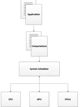
Compute intensive applications (including stock market evaluation, weather prediction, and medical diagnosis) often have impractical execution times when implemented using traditional CPUs. This leads to alternative hard-ware implementation in GPUs or FPGAs being required. These devices can be used alongside CPUs in order to increase performance. Individual computations can be assigned to different devices using a system scheduler controlled by a CPU. The resulting design is a heterogeneous system. An example of such a heterogeneous system is presented in Figure 1.1. The computations of these applications oftentimes consist of linear algebra op-erations such as matrix inverse, matrix decomposition, matrix-vector multi-plication, and matrix-matrix multiplication [13].
A number of choices must be made in order to select the hardware im-plementation that provides the best performance. The first is the selection of the device that will perform the computation. Both GPUs and FPGAs have been shown to be suitable alternatives to CPU implementations. This is due in part to their ability to perform operations simultaneously and to more directly control the execution of operations. Additional factors also con-tribute to device selection including the range of the input data, the required precision, and the available memory bandwidth.
2
[image:12.612.175.452.194.560.2]such as hardware area and available memory bandwidth of the system influ-ence these choices. Given the variability in these factors, there is a demand for a large variety of FPGA accelerators in order to meet the performance demands of different systems. The traditional process of developing a fully custom FPGA accelerator limits the practicality of such an approach.
Figure 1.1: Example of a heterogeneous system utilizing CPU, GPU, and FPGA.
Technologies and Vivado HLS which is supported by Xilinx [4]. A custom implementation is developed as a specific architecture that optimizes perfor-mance through direct control of the amount of hardware resources dedicated to the accelerator. A variety of synthesis tools exist for use in designing a custom implementation including ones supported by Xilinx, Altera, and Synopsys.
An area yet to be explored is the difference in performance, design time, and resource utilization between the two design techniques. In order to ob-tain realistic results, it is necessary to choose a medium for comparison. As mentioned previously, linear algebra operations consitute a large percentage of the computations within a class of applications that could benefit from implementation on a heterogeneous system. Among these, matrix-matrix multiplication stands out as a premier candidate for examination due to its exploitable parallelism and variety of different algorithms. The inherent paralellism is important because it gives incentive to implement the com-putation on an FPGA rather than on a CPU. The multitude of algorithms is important because implementing different algorithms provides additional information on how they vary under different circumstances.
The purpose of this work is to research new techniques of hardware de-velopment in order to improve the efficiency of accelerator design for use in hetereogeneous systems. This is accomplished through the design of three distinct matrix multiplication algorithms (standard, Strassen, and sparse ma-trices) using three different design techniques (software, HLS, and custom). The goals for the software portion of this work are to design and test successful implementations of each of the three algorithms. The algorithms were implemented in C++ on an Intel Core i7 Sandy Bridge 3.4 GHz pro-cessor. The designs operated on integers for simplicity.
4
Many of the directives improve run time at the cost of consuming additional FPGA resources. Thus a careful balance must be struck between increasing the performance of the multiplier and straining the resources of the FPGA. The run time results are saved using the provided evaluation metrics within the HLS tools.
The custom implementation section of the work begins with research-ing and understandresearch-ing the three designs described in the references [5], [2], and [11]. Each algorithm must be individually examined and implemented through architecture design and HDL modeling. The design of each custom implementation is modeled after was has been descibed in the background section with minor modifications. Each of the designs are developed for im-plementation on the target platform, the Xilinx XC6VSX475T. Every algo-rithm implementations is designed for operating on 32 bit precision integer operands. The run time results are determined through implementation of each custom design.
Chapter 2
Supporting Work
2.1
FPGA Overview
[image:15.612.103.539.426.667.2]FPGAs consist of a set of reconfigurable resources that can be configured to implement particular function. The resources consist of configurable logic blocks (CLBs), input-output buffers (IOBs), digital clock managers (DCMs), digital signal processor slices (DSPs), and block rams (BRAMs). A high level overview of an FPGA is presented in Figure 2.1 [6]. Figure 2.2 shows the contents of an FPGA configurable logic block [8]. The compo-nents of an FPGA slice are presented in Figure 2.3 [8].
6
Figure 2.2: Example contents of a configurable logic block within a Xilinx FPGA [8].
[image:16.612.164.457.377.642.2]FPGAs are very efficient for use in use in digital signal processing appli-cations due to their highly parallel nature and ability to implement custom algorithms. Applications that require many binary multipliers and adders are best implemented using dedicated DSP slices. DSP slices contain built-in cascade logic that allows multiple DSP slices to be connected together in order to implement complex functions. Without this ability the FPGA would have to develop large and inefficient adder trees to implement this functionality. A diagram demonstrating the basic functionality of the DSP slices present in the Virtex 6 is presented in Figure 2.4 [9].
Figure 2.4: Example architecture of DSP slice on a Xilinx FPGA [9].
8
Figure 2.5: Architecture of the Xilinx memory interface [10].
The user interface block provides a simple interface to the memory com-ponent from the user logic. It also buffers all read and write data. In addi-tion, it reorders the read return data to match the request order and presents a flat address space to the user that it translates to the address space required by the memory.
The memory controller block receives the requests from the user design and reorders them to minimize stall states. This feature serves to increase the performance of the memory component. It also performs high level management functions such as refresh and activate/precharge.
The physical block interfaces with the memory controller block and trans-lates the internal signals into the actual signals that connect to the memory component. This block also synchronizes the control signals and data over the various clock domains. In additon, it also performs the necessary initial-ization and management of the memory device.
2.2
Design Methodologies
2.3
Custom Design Flow
Figure 2.6: Example flow for custom FPGA design using traditional hardware description languages [7].
10
necessary timing contraints of the implementation. Finally, a timing sim-ulation is performed which evaluates the design with all timing constraints implemented. After design implementation the FPGA is programmed with the resulting bitstream and on-chip verification is performed.
2.4
HLS Design Flow
[image:20.612.115.511.253.616.2]The design flow for an HLS design is presented in Figure 2.7 [4].
Figure 2.7: Example flow for FPGA design using the Vivado HLS tool [4].
as functional. From this point the code is imported to the HLS tools. Op-tionally, directives can be added which can alter performance and resource consumption. Directives will be discussed in more detail further in the doc-ument. A register-transistor logic (RTL) wrapper is developed using the HLS tools which can be used to verify the design. Once the design is suc-cessfully verified it can be packaged and exported in a convenient fashion for use in an exisiting system.
2.5
Matrix Multiplication Algorithms
2.6
Standard Algorithm
The standard algorithm for matrix-matrix multiplication multiplies each el-ement of each row in input matrix A with each element of each column in input matrix B [5]. The results of each row/column combination are summed, whichs results in an element of output matrix C. The algorithm is demonstrated in Figure 2.8. This particular algorithm requires n×m × p
elementary multiplications and additions, where m and n are the number of rows and columns in matrix A and n and p are the number of rows and columns in matrix B. For the special case in which bothAandB are square matrices, the number of additions and multiplications are both equal to N3, whereN is the number of rows and columns in bothAand B.
A =
a1,1 a12 . . . a1,n
a2,1 a2,2 . . . a2,n
..
. ... . .. ...
am,1 am,2 ... am,n B =
b1,1 b1,2 . . . b1,p
b2,1 b2,2 . . . b2,p
..
. ... . .. ...
bn,1 bn,2 ... bn,p C=
c1,1 c1,2 . . . c1,p
c2,1 c2,2 . . . c2,p
..
. ... . .. ...
cm,1 cm,2 ... cm,p
C =A×B ci,j =
n X
k=1
(ai,k ×bk,j)
12
2.7
Block Multiplication
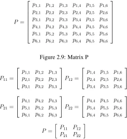
Block based multiplication is a method of matrix-matrix multiplication that is particularly useful for parallel based implementations. In order to perform this method of multiplication, it is necessary to partition the source matrices into separate smaller matrices called blocks. Figure 2.9 shows a matrix P
with 6 rows (m) and 6 columns (n) of elements [12]. Figure 2.10 shows the process of partitioning matrix P into blocks. The block extends until it reaches a limit of elements defined by BB, the basic block size. In this example, BB = 3.
Figure 2.11 shows the procedure of performing block multiplication. The resulting matrix C is developed from performing operations on blocks as opposed to individual elements.
P =
p1,1 p1,2 p1,3 p1,4 p1,5 p1,6 p2,1 p2,2 p2,3 p2,4 p2,5 p2,6 p3,1 p3,2 p3,3 p3,4 p3,5 p3,6 p4,1 p4,2 p4,3 p4,4 p4,5 p4,6 p5,1 p5,2 p5,3 p5,4 p5,5 p5,6 p6,1 p6,2 p6,3 p6,4 p6,5 p6,6
[image:22.612.180.437.345.627.2]
Figure 2.9: Matrix P
P11=
p1,1 p1,2 p1,3 p2,1 p2,2 p2,3 p3,1 p3,2 p3,3
P12 =
p1,4 p1,5 p1,6 p2,4 p2,5 p2,6 p3,4 p3,5 p3,6
P21=
p4,1 p4,2 p4,3 p5,1 p5,2 p5,3 p6,1 p6,2 p6,3
P22 =
p4,4 p4,5 p4,6 p5,4 p5,5 p5,6 p6,4 p6,5 p6,6
P =
P11 P12 P21 P22
C =A×B
C11 C1N
CN1 CN N
=
A11 A1N
AN1 AN N
×
B11 B1N
BN1 BN N
Cij = N X
k=1
Aik×Bkj
Figure 2.11: Example of matrix block multiplication.
2.8
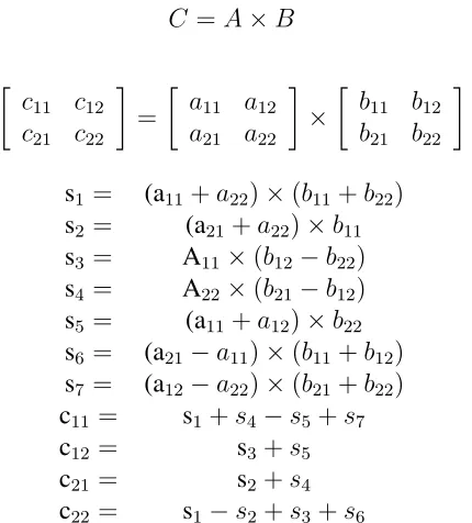
Strassen Algorithm
The Strassen algorithm operates on2×2matrices and is designed to reduce the number of multiplications operations at the expense of requiring addi-tional summations [2]. Intermediary results s1−s7 are defined as functions
of the input elements a11 −a22 and b11 −b22. The output results c11 − c22
14
C =A×B
c11 c12 c21 c22
=
a11 a12 a21 a22
×
b11 b12 b21 b22
s1 = (a11+a22)×(b11+b22)
s2 = (a21+a22)×b11
s3 = A11×(b12−b22)
s4 = A22×(b21−b12)
s5 = (a11+a12)×b22
s6 = (a21−a11)×(b11+b12)
s7 = (a12−a22)×(b21+b22)
c11 = s1+s4−s5+s7
c12 = s3+s5
c21 = s2+s4
[image:24.612.204.419.86.324.2]c22 = s1−s2+s3+s6
Figure 2.12: General description of the Strassen matrix multiplication algorithm.
2.9
Sparse Matrices Algorithm
S =
0 s1,2 0 0
0 s2,2 s2,3 0 s3,1 0 0 s3,4 s4,1 0 0 0
val s1,2 s2,2 s2,3 s3,1 s3,4 s4,1
col 1 1 2 0 3 1
row 0 1 3 5
val s3,1 s4,1 s1,2 s2,2 s2,3 s3,4
row 2 3 0 1 1 2
col 0 2 4 5
Figure 2.13: Example sparse matrix (top) compressed in CSR (middle) and CSC (bottom) formats.
2.10
HLS
HLS is a fairly new form of accelerator development that converts C and C++ software into a hardware design. HLS tools have numerous means available which allow for adjusting the architecture of the algorithms for the FPGA platform. The primary method of improving performance is to apply directives to a design. Directives are commands that instruct the HLS tool to implement special functions to an HLS Design. One such directive is loop pipelining. When used on a loop within the HLS tool, the pipeling di-rective allows different loop iterations to overlap in time. Figure 2.14 shows a simple loop that performs three different operations. Table 2.1 shows how the loop would be executed with no directives (architecture control). Table 2.2 displays the execution of the loop after applying the pipelining directive [4].
Clock Cycle 1 2 3 4 5 6
Operation read op compute op write op read op compute op write op
16
void function(...) {
for(i=0;i<=1;i++) {
read_op; compute_op; write_op; }
}
Figure 2.14: Example loop to be pipelined.
Clock Cycle 1 2 3 4
Operation read op compute op write op
Operation read op compute op write op
Table 2.2: Example loop execution (pipelined).
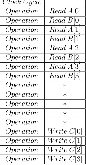
Another example of an HLS directive is loop-unrolling. Loop-unrolling separates for-loops into multiple independent operations rather than a single group of operations. Loops can be unrolled fully or partially. Figure 2.15 shows a multiplication operation performed over 4 iterations of a for-loop. Table 2.3 shows how the loop would be executed with no architecure con-trol. Table 2.4 displays the execution of the loop after applying the unroll directive with a factor of 2. Table 2.5 shows the loop execution after fully unrolling it [4].
void function(...) {
for(i=0;i<=3;i++) {
C[i] = A[i] * B[i]; }
}
Clock Cycle 1 2 3 4
Operation Read A[0] Read A[1] Read A[2] Read A[3]
Operation Read B[0] Read B[1] Read B[2] Read B[3]
Operation ∗ ∗ ∗ ∗
[image:27.612.241.380.367.632.2]Operation W rite C[0] W rite C[1] W rite C[2] W rite C[3]
Table 2.3: Example Loop Execution (No Architecture Control)
Clock Cycle 1 2
Operation Read A[0] Read A[2]
Operation Read B[0] Read B[2]
Operation Read A[1] Read A[2]
Operation Read B[1] Read B[2]
Operation ∗ ∗
Operation ∗ ∗
Operation W rite C[0] W rite C[2]
Operation W rite C[1] W rite C[3]
Table 2.4: Example loop execution (unrolled factor = 2)
Clock Cycle 1
Operation Read A[0]
Operation Read B[0]
Operation Read A[1]
Operation Read B[1]
Operation Read A[2]
Operation Read B[2]
Operation Read A[3]
Operation Read B[3]
Operation ∗ Operation ∗ Operation ∗ Operation ∗ Operation ∗ Operation W rite C[0]
Operation W rite C[1]
Operation W rite C[2]
Operation W rite C[3]
Table 2.5: Example loop execution (fully unrolled).
18
number of hardware components necessary for the HLS design. This in turn can reduce the maximum operating clock frequency by creating a larger longer critical path through the design, reducing performance.
2.11
Custom
An interesting custom implementation of the standard algorithm has been studied in [5]. In said work matrix-matrix multiplication is identified as a major bottleneck in facial recognition systems. According to the research, in a sample of facial recognition algorithms examined over eighty percent of the computation time was spent on matrix multiplication [5].
The technology of choice for this work was the Virtex 5 VSX240T. The reference architecture was designed to perform the two innermost for-loops of the standard algorithm in parallel. This means that N ×N multiplica-tions and addimultiplica-tions were performed simultaneously. However, as the matrix multiplication was performed on a block by block basis, N in this case did not refer to the size of a source matrix, but rather the size of the matrix block that is being computed. As such, this value is referred to as the basic block size (BB) andN maintains its original meaning as the size of an input matrix. In their work BB = 16, meaning that BB2 = 162 = 256 elemen-tary multiplications and additions were performed simultaneously. Thus this implementation performs the standard algorithm by partitioning the in-put matrices into blocks of sixteen elements and then repeatedly performing calculations until the full matrix computation is complete. The result is a matrix multiplication computation that was claimed to be more than fourty times faster than similar systems implemented previously on reconfigurable devices. Table 2.6 shows the experimental results from [5]. Table 2.16 shows an example implementation with N = 2and BB = 2.
M atrix Dimensions Execution T ime(ms) (64,64)×(64,64) 0.022
[image:29.612.156.465.97.446.2](128,128)×(128,128) 0.071 (256,256)×(256,256) 0.454 (512,512)×(512,512) 3.645 (1024,1024)×(1024,1024) 29.063
Table 2.6: Results from [5].
a11 a12 a21 a22
×
b11 b12 b21 b22
=
c11 c12 c21 c22
Figure 2.16: Standard algorithm implementation with N=2 and BB=2.
and used to compute the blocks of the result matrix. Several of these mul-tipliers were used simultaneously in order to speedup the run time of the matrix multiplication computation. The number of2×2multipliers used is the basic element (BE) count.
20
BE = 4 andN = 4.
M atrix Dimensions Execution T ime(ms) (8,8)×(8,8) 0.035
[image:30.612.186.434.290.539.2](32,32)×(32,32) 0.120 (64,64)×(64,64) 1.523 (256,256)×(256,256) 100.562 (512,512)×(512,512) 945.312
Table 2.7: Results from [2].
Figure 2.18: Example of Strassen implementation with BE=4 and N=4.
Some work has been presented on sparse matrix multiplication imple-mented on FPGAs. A design of interest is that presented in [11]. The Xilinx XC5VLX110T FPGA was the technology utilized for this work. The cho-sen architecture for this particular implementation is that of a systolic array. The systolic array consists of processing elements (P Es) that pass data back and forth between one another in order to keep off-chip memory accesses to a minimum. The P E is defined as a multiply-accumulator, three memory elements, registers, and control logic. Like the other custom implementa-tions, this design relies on block-based multiplication in order to perform large matrix-matrix multiplication computations. The focus of this work is on balancing the power-delay product and the energy-delay product. The power-delay product is used to estimate the tradeoff between energy con-sumption and delay. The energy-delay product indicates the tradeoff be-tween performance (run time) and energy consumption of the system.
This work found that there were two defining parameters of importance when designing the sparse matrix multiplier. These were the number of
22
was achieved when utilizing a smaller number of P Es and a smaller block size. Contrarily, a better energy-delay product is obtained by using a large number of P Es and a large basic block size. Tables 2.8 - 2.11 display the experimental results presented in [11]. Figure 3.4 shows the design of the sparse processing element. Figure 3.5 shows an example implementation with a variable number of processing elements.
N umber of P Es Density = 100 30 20 10 4 30.5 38.1 39.5 48.2 8 18.0 25.0 28.1 37.3 16 13.2 24.8 29.1 29.5 32 10.0 22.1 29.5 52.1 64 9.4 26.2 37.5 80.8
Table 2.8: Power-delay product (in mW×cycles/operation) versus number of PEs.
N umber of P Es Density= 100 30 20 10 4 7.90 11.80 13.6 18.1 8 2.10 4.62 5.90 9.90 16 1.00 3.10 4.00 9.50 32 0.33 2.00 3.52 9.80 64 0.12 1.90 3.82 16.02
Table 2.9: Energy-delay product (in mJ×cycles/operation) versus number of PEs.
Block Size Density = 100 30 20 10 96 7.50 19.50 26.11 54.30 128 7.41 16.23 21.12 39.19 192 10.00 19.94 31.12 39.17 256 13.21 25.02 29.82 44.32 384 24.13 39.98 45.14 64.21
Block Size Density= 100 30 20 10 4 0.51 4.11 7.11 24.96 8 0.48 2.51 4.92 14.21 16 0.51 2.54 4.56 9.93 32 0.63 3.12 4.71 9.84 64 2.12 4.95 4.08 10.44
[image:33.612.144.483.243.457.2]Table 2.11: Energy-delay (in mJ×cycles/operation) versus block size.
Figure 2.19: Design of sparse matrices Processing Element (PE).
24
Chapter 3
Custom Implementations
3.1
Standard Implementation
The standard custom design was implemented using a block-based multipli-cation technique in an effort to best take advantage of the FPGA hardware. The product of large matrices is obtained through performing the multipli-cation and summation the blocks they are composed of. The size of these blocks is designated by BB. The standard algorithm is performed on the blocks until the final result for the operation is acquired. The number of iterations through the matrix multiplier necessary to compute the final re-sult is represented by (N/BB)3 where N is the source matrix size. For this particular design, the decision was made to perform the two innermost for-loops of the standard algorithm in parallel. This meant that the number of simultaneous operations performed was equal to BB2. Thus a small in-crease in basic block size resulted in a large inin-crease in resources consumed. In this implementation the basic block size was chosen to be 16, meaning that 256simultaneous multiplications and additions were performed.
Figure 3.1: Custom standard matrix multiplier compute logic with BB=16.
3.2
Strassen Implementation
The Strassen custom implementation design began with the designation of a basic element, BE, as a2×2multiplier as depicted in Figure 3.2.
TheBEcalculates the intermediary matricesS1−S7as described in the Strassen algorithm. These matrices are then then summed in order to pro-duce the resulting output matrix. This design connected four BEsin paral-lel in order to more efficiently complete a 4×4matrix multiplication. Com-puting a 4×4 operation using only a single BE would take (43)/(23) = 8
iterations. Given that four multipliers were used in parallel, only 8/4 = 2
26
Figure 3.2: Design of Strassen basic element.
Figure 3.3: Custom Strassen compute logic with BE=4.
3.3
Sparse Implementation
[image:36.612.174.446.338.561.2]28
[image:38.612.139.483.143.359.2]Figure 3.4: Design of sparse matrices Processing Element (PE).
Chapter 4
HLS Implementations
4.1
Standard Implementation
Figure 4.1 shows the standard multiplication algorithm as it was imple-mented using the HLS tools.
fori= 0 →rows(A)do .Rows
forj = 0 →cols(B)do .Cols
fork = 0→rows(B)do .Product
Ci,j =Ci,j +Ai,k ×Bk,j .Calculation
end for end for end for
Figure 4.1: Standard matrix multiply algorithm implementation.
The source code consisted of three nested for-loops. In order to easily distinguish between the loops they were each assigned a label: Rows, Cols,
and P roduct respectively. This is important because the architecture
30
this particular design loop-unrolling and pipelining were chosen as mod-ifications to be made. Loop-unrolling is the premier choice for a design that features nested for-loops as it separates the loops into separate opera-tions that can be performed independently. The pipelining directive adds efficiency by adding registers which are used to more efficiently load data into the design. It should also be noted that pipelining a top-level for-loop unrolls all for-loops nested within the top-level loop. As previously men-tioned, these directives are applied on a loop-by-loop basis which allows easy manipulation of FPGA resource consumption. For loop unrolling in particular, an additional option exists (called factor) that allows partial un-rolling of a loop, which can further preserve resources. It is also important to keep in mind that when a top-level for-loop is unrolled all loops within the for-loop are also unrolled. With these ideas in mind, various versions of the HLS design were implemented. First, the pipeline directive was ap-plied to the P roduct loop. This was followed by pipelining the Cols and
Rows loops. The next step was to apply various levels of loop-unrolling to the accelerator. The initial loop to be unrolled was the P roduct loop. This was followed by the unrolling of the Cols loop. Both of these loops were fully unrolled. However, due to the limited number of DSP slices on the FPGA the third loop, Rows, could not be fully unrolled. As such, it was only partially unrolled with factors of2and4. Figures 4.2 - 4.3 show exam-ples of the RTL generated from a couple of the different variations Standard HLS design. The number of multiplexers, shift registers, multipliers, and adders varied depending on the directives applied to the design. Table 4.1 demonstrates the impact that the different directives had on the design of the hardware accelerator.
Figure 4.2: Standard HLS compute logic: no architecture control.
Figure 4.3: Standard HLS compute logic: cols pipelined.
Standard F actor M ult Add/Sub 32Bit Reg 8Bit M ux Shif t Reg
N o A.C. N.A. 1 1 7 0 9
P roduct P ipelined N.A. 1 1 7 1 10
Cols P ipelined N.A. 2 6 18 36 18
Rows P ipelined N.A. 16 20 128 0 144
P roduct U nrolled 16 2 6 18 40 18
Cols U nrolled 16 32 35 252 295 288
Rows U nrolled 2 182 202 1311 316 1638
Rows U nrolled 4 506 493 3519 378 4600
Table 4.1: Standard HLS component utilization.
32
4.2
Strassen Implementation
Unlike the standard design, the Strassen implementation was not based di-rectly on an existing software implementation. Instead, the Strassen HLS design was approached with the desired hardware in mind rather than the sofware. The resulting code is presented in Figure 4.2.
fori= 0 →1)do .Outer
forj = 0 →1do .Mid
fork = 0→1do .Inner
A0 =A2i:2i+1,k:k+1 B0 =B2k:2k+1,j:j+1 S1 = (A011+A
0
22)×(B 0 11+B
0 22) S2 = (A021+A
0
22)×B 0 11 S3 =A011×(B12−B220 ) S4 =A022×(B21−B120 ) S5 = (A011+A
0
12)×B 0 22
S6 = (A021−A011)×(B110 +B120 ) S7 = (A012−A
0
22)×(B 0 21+B
0 22) C110 =C110 +S1+S4−S5 +S7 C120 =C120 +S3+S5
C210 =C210 +S2+S4
C220 =C220 +S1−S2+S3 +S6
end for
C2i:2i+1,2j:2j+1 =C2i:2i+1,2j:2j+1+C0
[image:42.612.102.321.200.518.2]end for end for
Figure 4.4: Strassen matrix multiply algorithm implementation.
The two inner-most for-loops work together to create the BEs of the hardware design. The outer-most exists to provide the functionality of the multiplexer in 3.3, that is, to provide two 2 × 2 matrices in series to be operated on.
to the custom design. However, the HLS design has the advantage of be-ing able to unroll the outer-most loop. In theory this would utilize more hardware resources than the custom design and provide a performance ad-vantage.
[image:43.612.97.529.385.550.2]As with the standard algorithm, various versions of the Strassen algo-rithm were examined. The first implementation tested was the HLS design with no architecture control added. The second was the design with the bot-tom level for-loop (Inner) pipelined. This was followed by the pipelining of the M iddle and Outer loops. The next stage of improvement was un-rolling each of the loops presented in the source code. As before, each of the loops (beginning with Inner) were successively unrolled for a total of three additional implementations. Each of the loops was fully unrolled, as the resource consumption was not as high as in the standard algorithm im-plementation. Figures 4.5 - 4.6 show two of the variations in RTL generated from the Strassen HLS design. Table 4.2 displays the component usage for each of the different HLS Strassen implementations.
Figure 4.5: Strassen HLS compute logic: no architecture control.
As mentioned above, the BE computes the matrix multiplication for a 2x2 matrices. The loop bounds were set for a 8x8 matrix, and so unrolling
the Innerloop produced two BEs and unrolling theMid loop produced four
34
Figure 4.6: Strassen HLS compute logic: mid unrolled.
Strassen M ult Add/Sub 32Bit Reg 32Bit M ux 4Bit M ux
N o A.C. 7 22 54 5 16
Inner P ipelined 7 21 63 6 20
M iddle P ipelined 14 40 111 5 20
Outer P ipelined 28 68 197 10 30
Inner U nrolled 14 40 102 5 25
M iddle U nrolled 28 70 193 8 34
[image:44.612.93.528.91.247.2]Outer U nrolled 56 120 367 22 2
Table 4.2: Strassen HLS component utilization.
Mid andInner loops.
4.3
Sparse Implementation
For the sparse matrices implementation,AandBwere input to the hardware function in compressed sparse row and compressed sparse column form re-spectively. The code consisted of 3 nested for loops, as with other imple-mentations. It is presented in Figure 4.3.
fori= 0 →rows(A)do .Top
forj =rowA[i]→rowA[i+ 1]do .Mid1
fork = 0→cols(B)do .Mid2
form=colB[k]→colB[k+ 1]do .Bottom
ifcolA[j] ==rowB[m]then
Ci,k =Ci,k +valA[j]×valB[m]
[image:45.612.104.351.87.250.2]end if end for end for end for end for
Figure 4.7: Sparse matrix multiply algorithm implementation.
difference between sequential elements in the row pointer array of matrixA. The bottom for-loop needed to be repeated for each non-zero element in a particular column of B. This value was found by subtracting the values of adjacent elements in the column pointer array of matrix B.
The HLS sparse matrices implementation differed from the other HLS designs in that the middle and bottom loops iterated for a number of times based on an input. Thus the number of iterations for the two were variable. This prevented directives such as unroll and pipeline from having any effect on the performance of the implementation. Figure 4.8 shows the RTL from the HLS sparse matrix multiplier. Table 4.3 provides more details as to the actual hardware utilized.
[image:45.612.99.537.500.655.2]36
Sparse 32Bit M ult 32Bit Add 32Bit Adder 32Bit M ux 32Bit Comp 4Bit M ux
N o Directives 1 1 73 1 32 44
Table 4.3: Sparse HLS component utilization.
Chapter 5
System Design
[image:47.612.95.525.336.520.2]5.1
Overview
Figure 5.1 shows the top level design for implementing the hardware accel-erators.
Figure 5.1: Design of the system from a top level perspective.
In order to provide for additional read and write buffering of the built-in memories, pbuilt-ing-pong buffers were utilized withbuilt-in the matrix multiplier component as is displayed in Figure 5.2. Each ping-pong buffer consisted of
16 distinct Block RAM elements which allowed for 16 simultaneous trans-fers (8read and 8write).
38
Figure 5.2: Design of the multiplier component, including the ping-pong buffers used in-crease throughput.
(1/(400×106)) = 2.5 ns. Given that each of the accelerators performed
calculations on32bit operands, this data was better expressed as2operands every 2.5ns or 1operand every1.25 ns.
If an implementation required more operands per compute logic clock cycle then could be provided by a single memory component than a different approach other than connecting straight to external memory needed to be taken.
A pipeline was developed in order to satisfy those implementations that required large amounts of memory bandwidth. The first stage of the pipeline consisted of writing sub-matrices of size 64×64 to the built-in memories of the FPGA, located within the input ping-pong buffers of the multiplier component. The final stage of the top-level pipeline stored the resulting
64×64 matrix to external memories.
memory located in the output ping-pong buffer. Figure 5.3 shows the design of the pipeline.
Figure 5.3: Pipeline designed to meet the high memory bandwith needs of the various matrix multiplier components.
Since the periods of the first and third stages of the pipeline could be adjusted by adding or removing memory elements the second stage was the limiting factor of the design. Within the second stage, the second sub-stage was dependent on the design that was being implemented. However, the periods of the first and third sub-stages were static regardless of choice of design.
40
order to complete the64×64matrix multiplication(64/16)3 = 64iterations through the second stage of the pipeline are required. Given these con-traints, total number of cycles required for the second stage was calculated as presented in Equation 5.1.
#of Cycles = (#of Iterations+(#of SubStages−1))×Cycles of SubStage
(5.1) Since first stage of the described pipeline required a transfer of 2 64×64
matrices(AandB) the total number of operands that needed to be processed was 2×256×256 = 8192. Given that a single SDRAM element can provide a single operand every 1.25 ns, one SDRAM component can provide the requisite number of operands in8192×1.25 = 10240ns. A pair of SDRAM elements working in parallel can write the operands in 10240/2 = 5120 ns. The third stage of the pipeline required the transfer of only a single 64×64
matrix. Thus 1SDRAM completes the operation in 4096×1.25 = 5120ns or 2SDRAMs in2560 ns.
5.2
Pipeline Calculations
5.2.1 Standard Implementations
The compute logic for the custom standard design reads one row and one column of operands each cycle. The maximum clock frequency of the compute logic was found to be 213 MHz after implementation. At this speed each input required 16 operands every (1/(213×106)) = 4.69 ns or 1 operand every .29 ns. Given that reading directly could only provide an operand every 1.25 ns it was clear that the standard custom design required the buffering capability of the pipeline.
number of cycles for the second sub-stage was calculated as6 + 2 + 16 = 24
cycles. Recall that the latency of the first and second sub-stages was 34
cycles. Thus the latency of the stage was limited by the first/third sub-stages and was34cycles. The final cycle count for the second pipeline stage was then calculated as(64 + (3−1))×34 = 2244cycles.
The period of the second stage of the pipeline was calculated as2244× (1/(213×106)) = 10535 ns. Recall that utilizing a single SDRAM
compo-nent for the first stage of the pipeline results in a period of 10240ns. Thus in order to meet the period of the second stage of the pipeline only a single SDRAM to be used. The third stage period value of 5120 ns with a single SDRAM met the standard set forth by the second stage was therefore not a bottleneck in the design.
The best case maximum clock frequency obtained for any of the HLS standard matrix multipliers was 266 MHz. Thus the implementation re-quired 4 operands (2 for A and 2 for B) every 3.76 ns or 1 operand every
.94 ns. A single SDRAM component provided a single operand every 1.25
ns without any buffering. Thus 2 SDRAMs could be used to provide the operands to inputs A and B and implementation of the pipeline was not necessary.
5.2.2 Strassen Implementations
The custom Strassen implementation required 8operands from both Aand
B each cycle. Using the maximum clock frequency (107MHz) the number of operands required for a single input was calculated as 8 operand every
(1/(107×106)) = 9.36 ns or 1 operand every .58 ns. Thus the use of the
pipeline was necessary.
42
multiplications. Given the latencies of the IP cores recommended from Xil-inx, this totaled to 4×2 + 6 = 14cycles. One iteration through the Strassen
4×4 multiplier required 2 cycles worth of operands to complete. Thus the total number of cycles required to complete a 16×16 matrix multiplication was equivalent to2×64+14 = 142cycles. Given this value, the cycle count for the second pipeline stage was calculated as(64 + (3−1))×142 = 9372
cycles.
The number of cycles was used with the maximum clock frequency to calculate the period of the second stage of the pipeline as 9372×
(1/(107×106)) = 87,589ns. The first stage of the pipeline has a period of 10240 ns or5120 ns when1 or2SDRAMs are used respectively. Since the period with only 1 component falls well beneath the value for the second stage of the pipeline only a single SDRAM needed to be used in the first stage. The third stage of the pipeline also easily meets the value set by the second stage with a single SDRAM.
The best case maximum clock frequency obtained for any of the HLS Strassen matrix multipliers was 180 MHz. The Strassen HLS multiplier required 4 operands every 1/(180 × 106) = 5.54 ns or 1 operand every
1.385ns. Therefore a single SDRAM component capable of providing a32
bit operand every 1.25 ns could satisfy both inputs Aand B of the Strassen HLS implementation.
5.2.3 Sparse Implementations
A single SDRAM provides 32 bits every 1.25 ns. The maximum clock frequency for any of the custom sparse designs was 341 MHz. Unlike the other implementations, indices also needed to be read from memory. The maximum value for a index was 16, as the implementation was designed to operate on 16×16 matrices. Therefore each index needed to be4 bits wide (24 = 16 possible values). This meant that a total of 24 bits needed to be read from memory every (1/(341×106)) = 2.93ns. Thus in order to satisfy
The maximum clock frequency for the HLS sparse implementation was found to be 121 MHZ. Given that the design required 4 operands every
1/(165×106) = 6.04 ns and that single SDRAM provided an operand
44
Chapter 6
Results
6.1
Standard Results
The hardware resources consumed by each of the implemented standard designs are presented alongside the performance speedup compared to the software design in Table 6.1.
Pipelining the innermost loopP roductresulted in a speedup three times greater than that of the non-optimized design at the cost of very few re-sources. Likewise, pipeliningColsyielded a speedup five times greater than that of the P roduct pipelined implementation. On the contrary, pipelining the outermost loop Rows gave a noticeable increase in resource consump-tion with no improvement in speedup. This is due to the decrease in max-imum clock frequency associated with the increase in hardware utilization of the design.
Unrolling P roduct resulted in an improvement in speedup by a factor of seven with a minimal increase in resource consumption. However, the performance to resource compsumption ratio greatly decreases with addi-tional unrolls. Unrolling Cols decreased doubled the speedup of the design but at a cost of using five times the number of DSPs. This trend continued as an unroll of the Rows loop unrolled with a factor of 2yielded a slightly improves speedup but a DSP usage of 27 percent. Again this is due to the much lower maximum clock frequency of the larger designs.
Optimization Resources [Total] Speedup LUTs FFs DSPs
[297760] [595520] [2016]
None 1% 1% 1% 0.2x
ProductPipelined 1% 1% 1% 0.6x
ProductUnrolled 1% 1% 1% 3.2x
ColsPipelined 1% 1% 1% 3.2x
ColsUnrolled 1% 1% 5% 1.5x
RowsPipelined 1% 1% 2% 2.7x
RowsUnrolled - 2 3% 2% 27% 3.1x
RowsUnrolled - 4 7% 5% 75% 4.8x
[image:55.612.124.486.87.243.2]Custom 1% 1% 13% 50.6x
Table 6.1: Percent of resources utilized and speedup compared to software implementation of standard algorithm.
greatly decreased the clock frequency at which the designs could operate. This negated much of the performance gain from the decreased latency. This is due to the inefficiencies associated with the HLS tools in control-ling large designs. When the designs are small the HLS tools can easily generate a state machine that controls data flow fairly efficiently. However, when designs are larger the control logic auto-generated from the HLS tools is unable to handle the data efficiently, causing the much lower maximum clock frequencies.
The HLS design with the largest speedup compared to the software de-sign was the Rows Unrolled - 4 implementation which obtained a speedup of 4.8. The custom standard design achieved a speedup of 50.6, over 10
times greater than that of the Rows Unrolled - 4 implementation. In addition, the custom design utilized fewer resources than the Rows Unrolled
-4 implementation. Perhaps the most notable discrepancy between the two designs lays in the fact that the HLS design only reads2elements from each input matrix into its buffers simultaneously. Recall that in the ping-pong buffers used in the custom design a total of 8simultaneous reads were pos-sible. This difference meant that the custom implementation could read data
46
Optimization Resources[Total] Speedup LUTs FFs DSPs
[297760] [595520] [2016]
None 1% 1% 1% 0.4x
InnerPipelined 1% 1% 1% 0.5x
InnerUnrolled 1% 1% 2% 1.0x
MidPipelined 1% 1% 2% 2.0x
MidUnrolled 1% 1% 4% 1.6x
OuterPipelined 1% 1% 4% 2.0x
OuterUnrolled 1% 1% 8% 2.9x
Custom 1% 1% 6% 4.8x
Table 6.2: Percent of resources utilized and speedup compared to software implementation of Strassen algorithm.
6.2
Strassen Results
The hardware resources consumed by each of the Strassen implementations are presented alongside the speedup over the software implementation in Table 6.2.
The initial pipeling of the innermost loop did not result in a vast im-provement in speedup over the unoptimized design. Pipelining the M iddle
loop however yielded a 5times improvement over the Inner pipelined im-plementation. Contrarily, pipelining the loop Outer resulted in a notable increase in resource consumption with little improvement in speedup. This is due to simply the nature of the algorithm and how little it is impacted by pipelining. Pipelining the M iddle loop only provided a large increase in speedup because by default it unrolled the loop beneath it,Inner.
Unrolling Inner doubled the amount of DSP slices consumed and in-creased the speedup by a factor of 2. This trend continued as the unrolling of both the M iddle and yielded a doubling of consumed resources and approximate doubling of speedup. This is due to the decrease in latency associated with performing more the computation in parallel and the the steady maximum clock frequency across designs.
is clear that even the largest of Strassen implementations were still small compared to the large standard implementations. Thus the Strassens de-signs were small enough for the control logic auto-generated from the HLS tools to be efficient, resulting in a fairly constant maximum clock frequency across the different implementations. This meant that the decreased latency resulting from unrolling the algorithm directly correlated to an increase in speedup of the computation.
The M iddle unrolled implementation represents the attempt at
replicat-ing the exact hardware designed for the Strassen custom implementation through use of the HLS tools. Being able to compare the custom implemen-tation to an HLS counterpart that utilized the same number of elementary multipliers gave a unique opportunity to examine the differences in design. The first thing to note is that the the custom design uses 1.5times as many DSP slices as the HLS design. This is due to the optimizations made within the Xilinx Multiplier IP core of the custom design. The same problem with the number of simultaneous data reads that existed with the standard HLS design also exists with the Strassen HLS design. The ability of reading 2
operands simultaneously simply does not compete with the ability of the custom design to load 8operands into its buffer simultaneously.
6.3
Sparse Results
The speedup of the sparse matrix multiplier implementations over the soft-ware design are presented alongside hardsoft-ware resource usage in Table 6.3.
Optimization Resources[Total] Speedup[Density]
LUTs FFs DSPs
[297760] [595520] [2016] [30%] [20%] [10%]
None 1% 1% 1% 1.2x 1.0x 0.6x
Top Pipelined 1% 1% 1% 0.9x 0.8x 0.5x
Top Unrolled 12% 4% 1% 0.5x 0.4x 0.2x
Custom PE - 4 1% 1% 1% 223.9x 140.4x 56.7x
Custom PE - 8 1% 1% 2% 240.0x 132.0x 43.8x
Table 6.3: Percent of resources utilized and speedup compared to software implementation of sparse algorithm.
48
the HLS tool did not provide any performance boost over the non-optimized design. In fact, each of the tested optimized designs actually reduced the speedup nwhen compared to the non-optimized design. This is due to the additional control logic necessary to implement the optimizations. As pre-viously mentioned, control logic is a weakness of the HLS tools. The sparse algorithm, with its non-deterministic for-loops, is the most control inten-sive of the algorithms implemented. The only HLS design that managed a speedup greater than1.0was the non-optimized design in the case of matrix densities of 30. In general, as matrix density decreased the HLS designs became less efficient.
Chapter 7
Design Time Comparison
[image:59.612.147.464.329.554.2]The performance and design time of implementing each of the three matrix multiplication algorithms in software, HLS, and custom is shown in Figure 7.1.
Figure 7.1: Design time of matrix multiplication algorithms and their various implementa-tions.
50
each design. There is a clear pattern that can be established across the dif-ferent algorithms. In each case the software implementation had the low-est design time and the custom implementation had the longlow-est design time, with the HLS implementation falling in the middle. The degree to which the different implementations varied in design time depended on the algorithm. In the cases of the standard and sparse algorithms, where the HLS source codes were ported directly over from established software implementations, the gap was very large. This was due to the ease in transitioning from a functional software design to an HLS design.
The Strassen HLS implementation was designed to mimic the architec-ture of the developed Strassen custom design. The Strassen HLS design took significantly longer than that of the other two algorithms due to the fact that it wasn’t ported from an existing software design. However, the Strassen HLS design performs closest to its custom implementation when compared to the other two algorithms. Thus the additional design time of the Strassen HLS implementation yielded a net gain in performance.
Chapter 8
Combined Custom/HLS Design Flow
It is clear that while custom designs outperform HLS designs, they also take significantly longer to design. In general, this performance gap can be bridged by applying optimizations to the HLS designs, though cases exist (such as with the sparse algorithm case) in which the optimizations do not improve performance In addition, approaching HLS design from an angle alternative to porting over existing software code (such as was done with the Strassen algoritm) can also yield increased performance. With these conclusions in mind, a design flow such as presented in Figure 8.1 is rec-ommended.
The first step in the design flow would be to research the application and determine if there is any established software implementation that could be ported into the HLS tool. Next would be performing a check to make certain that the application is suitable for implementation using the HLS tool by checking for things such as non-deterministic loops. If it is not, then a custom design is necessary and the designer can move directly to following a design flow similar to that presented in 2.6. If no pitfalls are found and the application is deemed suitable for HLS implementation than the designer can move to following a HLS design flow similar to that shown in 2.7.
52
Figure 8.1: Example of an efficient design flow for developing applications on the FPGA.
Chapter 9
Conclusions
54
Bibliography
[1] Nathan Bell and Michael Garland. Implementing sparse-matrix-vector
multiplication on throughput-oriented processors. In Proceedings of the Conference on High Performance Computing Networking, Storage
and Analysis, 2009.
[2] Ignacio Bravi, Jimenez Pedro, Jose Luis Lazaro, Jose de las Heras, and
Alfredo Gardel. Different proposals to matrix multiplication based on FPGAs. In IEEE International Symposium on Industrial Electronics, 2007.
[3] Thomas Cormen, Charles Leiserson, Ronald Rivest, and Clifford
Stein. Strassen’s algorithm for matrix multiplication. In Introduction
to Algorithms, 2001.
[4] Wim Meeus, Kristof Van Beck, and Toon Goedeme. An overview of today’s high-level synthesis tools. In Springer Science and Business
Media, 2012.
[5] Ioannis Sotiropoulos and Ioannis Papaefstathiou. A fast parallel matrix multiplication reconfigurable unit utilized in face recognition systems.
InInternational Journal of Computer Applications, 2009.
[6] Prasanna Sundararajan. High performance computing using FPGAs.
InWhite Paper: FPGAs, 2010.
[8] Xilinx. Virtex-6 FPGA configurable logic block. InUser Guide, 2012.
[9] Xilinx. Virtex-6 FPGA DSP48E1 slice. In User Guide, 2012.
[10] Xilinx. Virtex-6 FPGAs memory interface solutions. In User Guide, 2012.
[11] Colin Yu Lin, Zheng Zhang, Ngai Wong, and Hayden Kwok-Hay So.
Design space exploration for sparse matrix-matrix multiplication in FPGAs. In International Convference on Field-Programmable
Tech-nology, 2010.
[12] Ling Zhuo and Viktor Prasanna. Design tradeoffs for BLAS operations
on reconfigurable hardware. In International Conference on Parallel
Processing, 2005.
[13] Ling Zhuo and Viktor Prasanna. High performance designs for linear algebra operations on reconfigurable hardware. In Computers, IEEE
![Figure 2.1: Example set of reconfigurable resources available on a Xilinx FPGA [6].](https://thumb-us.123doks.com/thumbv2/123dok_us/108679.10094/15.612.103.539.426.667/figure-example-set-recongurable-resources-available-xilinx-fpga.webp)
![Figure 2.3: Example contents of a slice on a Xilinx FPGA [8].](https://thumb-us.123doks.com/thumbv2/123dok_us/108679.10094/16.612.183.442.91.334/figure-example-contents-slice-xilinx-fpga.webp)
![Figure 2.4: Example architecture of DSP slice on a Xilinx FPGA [9].](https://thumb-us.123doks.com/thumbv2/123dok_us/108679.10094/17.612.96.542.265.478/figure-example-architecture-dsp-slice-xilinx-fpga.webp)
![Figure 2.6: Example flow for custom FPGA design using traditional hardware descriptionlanguages [7].](https://thumb-us.123doks.com/thumbv2/123dok_us/108679.10094/19.612.144.473.85.461/figure-example-ow-custom-design-traditional-hardware-descriptionlanguages.webp)
![Figure 2.7: Example flow for FPGA design using the Vivado HLS tool [4].](https://thumb-us.123doks.com/thumbv2/123dok_us/108679.10094/20.612.115.511.253.616/figure-example-ow-fpga-design-using-vivado-hls.webp)
![Table 2.6: Results from [5].](https://thumb-us.123doks.com/thumbv2/123dok_us/108679.10094/29.612.156.465.97.446/table-results-from.webp)