1
Ge interface engineering using ultra-thin La
2O
3and Y
2O
3films: A study into the effect
of deposition temperature
I.Z. Mitrovic, a),1 M. Althobaiti,2 A.D. Weerakkody1, V.R. Dhanak2, W.M. Linhart2, T.D. Veal2, N. Sedghi1, S.
Hall1
1
University of Liverpool, Department of Electrical Engineering & Electronics, Brownlow Hill, Liverpool L69
3GJ, United Kingdom 2
University of Liverpool, Department of Physics and Stephenson Ihnstitute for Renewable Energy, Liverpool
L69 7ZF, United Kingdom
P.R. Chalker3
3
University of Liverpool, Department of Engineering, Brownlow Hill, Liverpool L69 3GH, UK
D. Tsoutsou4, A. Dimoulas4
4
NCSR Demokritos, MBE Laboratory, Institute of Materials Science, 153 10 Athens, Greece
Abstract
A study into the optimal deposition temperature for ultra-thin La2O3/Ge and Y2O3/Ge gate stacks has been
conducted in this paper with the aim to tailor the interfacial layer for effective passivation of the Ge interface. A
detailed comparison between the two lanthanide oxides (La2O3 and Y2O3) in terms of band line-up, interfacial
features and reactivity to Ge using medium energy ion scattering, vacuum ultra-violet variable angle
spectroscopic ellipsometry (VUV-VASE), X-ray photoelectron spectroscopy and X-ray diffraction, is shown.
La2O3 has been found to be more reactive to Ge than Y2O3, forming LaGeOx and a Ge sub-oxide at the interface
for all deposition temperature studied, in the range from 44C to 400C. In contrast, Y2O3/Ge deposited at
400C allows for an ultra-thin GeO2 layer at the interface, which can be eliminated during annealing at
temperatures higher than 525C leaving a pristine YGeOx/Ge interface. The Y2O3/Ge gate stack deposited at
lower temperature shows a sub-band gap absorption feature fitted to an Urbach tail of energy 1.1 eV. The latter
correlates to a sub-stoichiometric germanium oxide layer at the interface. The optical band gap for the Y2O3/Ge
stacks has been estimated to be 5.7 0.1 eV from Tauc-Lorentz modelling of VUV-VASE experimental data.
For the optimal deposition temperature (400C), the Y2O3/Ge stack exhibits a higher conduction band offset (>
2.3 eV) than the La2O3/Ge (~ 2 eV), has a larger band gap (by about 0.3 eV), a germanium sub-oxide free
interface, and leakage current (~ 10-7 A/cm2 at 1 V) five orders of magnitude lower than the respective La2O3/Ge
stack. Our study strongly points to the superiority of the Y2O3/Ge system for germanium interface engineering
to achieve high performance Ge CMOS.
a)
2
I. INTRODUCTION
The most recent studies1,2 strongly advocate that high performance Ge CMOS (Complementary Metal Oxide
Semiconductor) technology is feasible. This technology is attractive due to the Ge intrinsic high mobilities for
electrons (3900 cm2/Vs) and holes (1900 cm2/Vs) as well as the CMOS compactness (Ge-based n- and
p-channel MOSFETs). The smaller band gap of Ge (0.67 eV) has the potential for lower contact resistances
compared to Si, and is consequently more suitable for voltage scaling3. Sub-nm equivalent oxide thickness
(EOT) gate stacks are required to keep the intrinsically high performance of Ge. The focus is on finding suitable
high permittivity ()dielectric ( > 20) to form a gate stack with low interface state density and EOT. The most
perilous issue is engineering a high-quality interface between Ge and the high-dielectric, that is, passivation of
the Ge surface. An interfacial layer (IL) either intentionally or unintentionally formed during the high-
dielectrics deposition process is usually necessary for achieving high electrical performance of Ge-based MOS
devices4-6 but its presence has a significant effect on achieving the desired EOT; it must be as thin as possible
and preferably with as high a permittivity as can be achieved. The four most commonly used approaches7 for
forming thin ILs for Ge passivation are: (i) nitridation, (ii) Si-based schemes, (iii) S-based passivation and (iv)
GeOx (x 2) grown through thermal, ozone- or plasma-assisted oxidation. The peak electron mobility has been
dramatically improved in Ge n-channel MOSFETs over recent years2,8-12. The highest reported electron mobility
is now approaching 2000 cm2/Vs8-9,12. The key to this achievement has been mainly in interface state reduction
at the GeO2/Ge interface. Thermally grown GeO2 is the most natural choice13-18. A high-quality GeO2 IL
provides a possibility for both p- and n-type Ge channel FETs. However, it is worth recalling that GeO2 has high
water solubility, low desorption temperature (~ 430°C) and low dielectric constant of ~ 6. A detrimental Ge
sub-oxide transition layer at a GeO2/Ge interface can be expected19,20. Toriumi’s group has systematically
investigated8-11,21-22 the GeO2/Ge interface in terms of both thermodynamics and kinetics of the Ge oxidation
process. An extremely low density of interface states (Dit = 6×10¹⁰ eV-1cm-2) has been reported for relatively
thick (~ 20 nm) GeO2/Ge23 allowing for high performance Ge n-MOSFETs21; note that the high density of the
acceptor-type interface states has been found to degrade Ge n-MOSFET performance18, while it is not a concern
for Ge p-MOSFETs due to the position of the charge neutrality level in Ge. An apparent degradation of drive
current has been observed when the GeO2 thickness has been further reduced3. A reduction in electron mobility
to 265 cm2V-1s-1 has been reported when the GeO2 IL is ~ 1.2 nm24. Oxygen plasma treatment has been
proposed to form good quality ~ 5 nm GeO2/Ge interface at low substrate temperatures, due to the highly
reactive O radicals25,26, leading to demonstration of an extremely low midgap Dit of 4.5×10¹⁰ eV-1cm-2.
High-pressure oxidation and low temperature oxygen annealing have recently been suggested as the process recipes
for nearly ideal GeO2/Ge system8. It seems that low temperature oxygen annealing can work for repairing the
dangling bonds in GeO2/Ge, while high-pressure oxidation suppresses the GeOx desorption at higher
temperature27, resulting in robust and dense GeO2 on Ge.
For aggressive oxide scaling with EOT well below 1 nm, the combination of higher- oxide and ultra-thin GeO2
is required. A small amount of rare-earth (RE) metal introduction into the GeO2 interface layer has been shown
to dramatically improve the interface8. Rare earth metal ions in oxides generally have large polarizability28;
3
bonding at the interface with Ge, redistributing the electronic charge and reducing the electrical activity of the
interface states to produce good passivating properties29. Rare earth oxides (La2O3, Y2O3, LaLuO3, Dy2O3,
Gd2O3, CeO2) react strongly with the substrate resulting in catalytic oxidation of Ge and the spontaneous
formation of stable interfacial layers29-32. This high reactivity of Ge with high- oxide suggests the possibility of
GeOx-free gate stacks. Another passivation route is to introduce a robust, ultra-thin high-k IL barrier, such as
Al2O31,33-37 or Tm2O338,39. It is worth noting here that the Ge surface passivated with Al2O3 is slowly oxidized
without causing GeOx diffusion or desorption. As a result, all the Ge atoms near the interface are terminated
with oxygen atoms or Ge atoms without any dangling bonds under the oxidation condition lower than 4+,
leading to low Dit even with GeOx IL. Peak electron and hole mobilities of 689 cm2/Vs and 546 cm2/Vs
respectively at EOT = 0.76 nm have been achieved by this approach for HfO2/Al2O3/GeOx/Ge gate stack1.
This paper focuses on the former Ge interface engineering approach using La2O3 and Y2O3 RE-oxides. These
high- oxides have moderate reactivity with Ge40 to form a germanate interface whose purpose is two-fold:
firstly to reduce the interface defects and secondly to suppress the GeOx desorption at the interface. GeOx-free
gate stacks constitute another advantage of this approach by choosing appropriate deposition conditions and
annealing procedures2. La2O3/Ge gate stacks have been investigated by a number of research groups41-49. It has
been shown48 that La changes the surface chemistry so that a stable LaGeOx compound is favoured against the
competing reaction of GeO2 with Ge, resulting in suppression of GeOx49. The stable La–O–Ge bond at the Ge
interface provides a surface-state “free” Ge band gap due to the fourfold coordination of La in the GeOx matrix
as predicted theoretically by Houssa et al.19 This allows for a gate stack with a low density of interface states (~
1011 eV-1cm-2) with nearly ideal electrical characteristics44,47. Moreover, internal photoemission (IPE)
experiments on ZrO2/La2O3/Ge MIS structures50 have indicated a sufficiently large conduction band offset
(CBO > 2 eV). Theoretical calculations using charge neutrality levels predict a LaGeOx band gap of 5 eV,
valence band offset (VBO) of 3 eV51, and CBO of La2O3 and Y2O3 on Ge of 2.56 eV52,53. The relative
permittivity ranges from 9-1244,54. It is worth mentioning that only La2O3 is reactive to water due to its
electropositive nature55,56 and may thus pose a challenge to the integration into a CMOS process flow.
Moreover, LaOx (x < 1.5) is only suitable for nFETs, because LaOx leads to an interfacial dipole in the gate
stack57. Passivation of Ge by La2O3 subsequently capped with ZrO2 results in stabilization of the tetragonal
crystalline ZrO2 phase47,58. The scaling potential of ZrO2/La2O3/Ge stacks to EOT values as low as 0.5 nm59 and
0.96 nm60 has been reported. The La2O3 deposition temperature has been found to have a noticeable effect on
the capacitance voltage (CV) characteristics44. The improved La2O3 electrical behaviour is obtained either by
depositing the material at higher temperature or by applying post-deposition annealing independent of ambient
(H2, N2, O2). The best characteristics (especially low Dit) have been obtained when these two conditions are
combined, although an increase in both leakage current and EOT has been observed44. There has been no
explanation of these observations from the structural and band line-up studies, and we address these issues in
this paper.
By contrast, Y2O3 is Ge-friendly and robust against water. An amorphous Y2O3 layer provides a wide bandgap
(~ 5.5-5.7 eV)56, high crystallization temperature (~ 2325°C), relatively high dielectric constant (~ 11–18)8,61-62
4
attributed to the stability of the Y2O3 interlayer in contact with the Ge substrate64. The mechanism for this
stability lies in the barrier role of the Y2O3 interlayer, which effectively blocks the inter-diffusion of Ge, thus
suppressing the growth of unstable GeOx and so improving the interface quality. Moreover, yttrium can also be
used to tune the overall effective work function of the gate stack through the formation of interface dipoles65. An
electron mobility of 1480 cm2/Vs for Y2O3/Ge n-MISFET has been demonstrated recently8. From XPS
measurements, the VBO of Y2O3/Ge has been found to be 2.78 eV and the band gap, 5.7 eV66. Formation of the
YGeOx affects leakage current, hysteresis, interface trap density, and other reliability issues that are important
for device operation9,40,61-62,66-67. The passivation effect of a YGeOx IL has been explained by so-called “valency
passivation”9; the introduction of yttrium atoms effectively suppresses the dangling bonds in the interfacial
region and consequently improves Dit in the range of 1011 cm-2eV-1 due to the trivalent RE nature of Y68-69.
Less is known, however, about the band line-up and structure of bulk and interfacial LaGeOx and YGeOx as a
function of deposition temperature, which is the main focus of this paper. A systematic study of the structural
properties of La2O3/Ge and Y2O3/Ge gate stacks as a function of deposition temperature has been conducted by
Medium Energy Ion Scattering (MEIS), X-ray Photoelectron Spectroscopy (XPS), Vacuum Ultra Violet
Variable Angle Spectroscopic Ellipsometry (VUV-VASE), and X-ray diffraction (XRD). The most significant
findings from the results which will be presented here are two-fold: firstly, evidence for the optimal deposition
temperature to tailor the interfacial layer for effective passivation of Ge interface; secondly, a comprehensive
comparison between the two lanthanide oxides (La2O3 and Y2O3) in terms of band line-up, interfacial features
and reactivity to Ge which points to the superiority of the gate stack for adoption in CMOS engineering.
II. EXPERIMENTAL
The 2 nm (nominal) La2O3/Ge and 5 nm (nominal) Y2O3/Ge gate stacks were deposited by Molecular Beam
Epitaxy (MBE) at temperatures ranging from 44C to 400C on n- and p-type Ge substrates. Prior to deposition,
the Ge surface was cleaned by a mild degreasing with trichloroethylene, acetone and methanol for 5 minutes in
each solvent to remove the organics. Then the GeOx native oxide was thermally desorbed in-situ, by annealing
at 450 – 500C for 30 minutes. The La2O3 films deposited at 44C and 250C were subjected to post-deposition
oxygen (O2) anneal at 300C for 15 minutes. Y2O3 films were prepared by co-deposition of Y and atomic
oxygen at temperatures 225C and 400C. The reference samples for spectroscopic ellipsometry and XPS
studies entailed a selection of thermally grown GeO2/Ge with/without capping Al2O3 layers, Al2O3/Ge as well as
oxidized La and Y foils. The GeO2 films of two nominal thicknesses 4.5 and 12 nm were prepared by ex-situ
furnace anneal at 450C for 5 min and 60 minutes respectively. The capping Al2O3 layers with 4 nm nominal
thickness were prepared in-situ by co-deposition of Al and atomic oxygen.
The X-ray photoelectron spectra for La2O3/Ge stacks were recorded at the Daresbury NCESS facility using an
ESCA300 spectrometer with monochromatised Al K X-rays of energy 1486.6 eV and electron take-off angles
(TOA) of 15-90°. The spectrometer was calibrated so that the Ag 3d5/2 photoelectron line had a binding energy
5
and the spectrometer pass energy was 150 eV with the entrance-slit width of the hemispherical analyzer set to
1.9 mm. Under these conditions, the overall spectrometer resolution was ~ 0.5 eV70. Charge compensation was
achieved using a VG Scienta FG300 low energy electron flood gun with the gun settings adjusted for optimal
spectral resolution. The electron BEs were then corrected by setting the C 1s peak in the spectra (due to stray
carbon impurities) at 284.6 eV for all samples71. Wide scans were recorded in the 0-1250 eV energy range to
determine the elements present in the samples and to check for surface contamination. Then the O 1s, Ge 3d, La
4d, and valence photoelectron lines were recorded separately. The core-level positions are defined as the
FWHM and determined to within 0.05 eV by fitting a Voigt curve to the measured peaks. A Shirley-type
background72 is used during the fitting of all the spectra. The angle resolved (AR)-XPS and measurements of
Y2O3/Ge stacks were made in a separate ultra high vacuum system consisting of an Al K X-ray source and a
PSP Vacuum Technology electron energy analyzer. This spectrometer was operated with an overall resolution
of about 0.8 eV. To diminish the effect of differential charging on evaluating valence band offset73-75, during the
XPS measurements the X-ray beam exposure was across the whole sample. The individual core level scans were
performed for the duration of at least an hour until the point at which they reached constant binding energies,
and the samples could be considered as charge saturated. Medium energy ion scattering was carried out at the
STFC Daresbury Laboratory, with a 100 keV He+ beam and a double alignment scattering configuration with a
scattering angles of 90° and 135.
The VUV-VASE measurements were performed using a spectral range from 0.5 – 8.8 eV (referring to
wavelength range = 140-2500 nm), and angles of incidence of 55-75°, by 10° as a step, to maximize the
accuracy. The entire optical path was enclosed inside a dry nitrogen purge to eliminate absorption from ambient
water vapour and oxygen. The XRD measurements were done using the Philips Xpert XRD system. Electrical
characterization was carried out at room temperature on metal insulator semiconductor (MIS) capacitors
patterned by Pt e-beam evaporation on the dielectric surface through a shadow mask consisted of circular dots
300 m in diameter. The back Ohmic contact was made using eutectic In-Ga alloy. The high frequency
capacitance voltage data were obtained with a HP4284 precision LCR meter.
III. RESULTS AND DISCUSSION
A. La2O3/Ge gate stacks
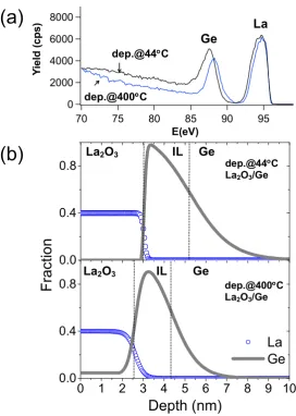
MEIS and XPS measurements were performed to assess the thickness, distribution of elements and interfacial
composition of the ultra-thin La2O3/Ge gate stacks. The key findings are outlined in this section. Note that as the
thicknesses were less than 5 nm, the results from spectro-ellipsometry on these stacks were not conclusive,
hence MEIS results were used. The MEIS energy spectra for the La2O3/Ge deposited at 44C and 400C are
shown in Fig. 1(a). There is a small high energy tail on the Ge signal for sample deposited at 400C that
indicates an inclusion of Ge in the La2O3 film. The elemental depth profiles were calculated assuming the
lanthanum signal is La2O3 with a stopping power density of 6.5 g/cm3. The calculated La and Ge depth profiles
are shown in Fig. 1(b), and reveal the structures of 3 nm La2O3/2.2 nm IL/Ge and 2.6 nm La2O3/1.7 nm IL/Ge
6
~ 9 Å for the gate stack deposited at higher temperature is evident. Note also a significantly broader edge to the
Ge substrate for the layer deposited at 44C, however a slightly narrower La2O3/Ge interface in comparison to
the sample deposited at 400C. The concentration of Ge (10-20%) in La2O3 sample deposited at 400C drops off
towards the surface. The results strongly point to the formation of Ge-rich interfacial layers. In the case of 44C
deposited sample, the top layer is La2O3, while strong intermixing (penetration of Ge) is visible for sample
deposited at higher temperature. It seems that bi-layer structure exists for the 44C deposited sample, with
germanate likely to be present at the interface. This observation is further underpinned by findings from the XPS
data.
It has been shown that La is strongly electropositive and tends to strongly attract neighbouring O atoms49. The
influence of La is considered to regulate the distribution of O in such a way that oxygen density is maximized in
the final compound48. Furthermore, La on Ge in the presence of oxygen has been found to produce only La–O
bonds19, with no gap states, and the formation of stable LaGeOx layers44,47-49. A penetration of Ge into the La2O3
layer observed in this work for the highest deposition temperature, is in agreement with the previous study44 by
energy dispersive X-ray spectroscopy where LaGeOx layer has been formed across the entire film at the
temperature of 360C.
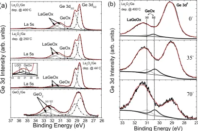
Fig. 2(a) shows the Ge 3d core level spectra for the 44C, 250C and 400C deposited stacks. The data were
fitted using a doublet of Voigt functions corresponding to Ge 3d5/2 and Ge 3d3/2 components. The spin-orbit
splitting and area ratio values of 0.6 eV and 2:3 were fixed for the fit. The spin-orbital splitting for Ge 3d
substrate peak (Ge 3d0) can be seen in Fig. 1(a) at energies of 28.6 and 29.2 eV. No presence of GeO2 at the
interface for La2O3/Ge stacks is evident from the Ge 3d core level spectra (see the reference GeO2/Ge spectrum
at the bottom of Fig. 2(a) for comparison); the Ge 4+ oxidation state has been reported to occur above 3 eV; @
3.2 eV49,76 and 3.4 eV77,78 from the Ge 3d0. Considering that the Gibbs free energy of formation of GeO2 (387
kJ/mol at 1000K), the GeO2 is thermodynamically unstable so that a GeO2 layer is unlikely to form at the
La2O3/Ge interface. Taking into account the electronegativity of Ge (2.01 using Pauling’s scale), LaGeOx is
expected to appear between the chemical shifts of GeO (Ge+2) and Ge2O3 (Ge+3), i.e. between 1.7 eV and 2.8
eV17,77. The energy shift of 2.2 eV for LaGeOx has been reported48,49. In our work, the presence of LaGeOx (3/2
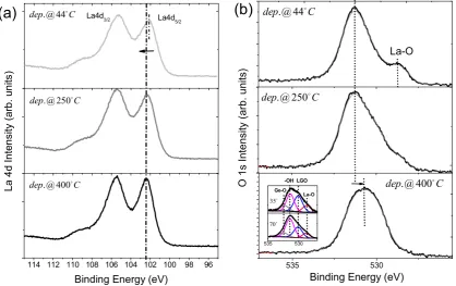
and 5/2) can be de-convoluted from the spectra at the chemical shift of +2.5 to +2.6 eV. Further evidence of
LaGeOx formation comes from the observed shift of La 4d5/2 doublet peak in Fig. 3(a) towards the higher BE (~
0.1-0.2 eV) in comparison to the pure La2O3 at 102.2 eV79. Note that the BE of La 4d5/2 for the 44C deposited
sample shows no shift in comparison to the pure La2O3, substantiating the MEIS result in Fig. 1(b) that this layer
consists mainly of lanthanum oxide. The O 1s spectrum shows further evidence of a clear La-O bond at 528.6
eV79 (see top graph in Fig. 3(b)), which flattens out as the deposition temperature increases, and the centroid
peak shifts towards lower binding energies for the 400C deposited sample consistent with a formation of
LaGeOx film44.
The Ge 3d spectra in Fig 2(a) confirm the existence of an interfacial layer ascribed to GeOx as the binding
energy shift lies at ~ 1.7 eV from the Ge 3d0. The reported values of Ge+1 and Ge+2 are at ~ 1 eV and 1.8 eV
7
Fig. 2(a)), while for higher deposition temperatures, the fitting shows only a very small single peak. The
angle-resolved XPS of this region for the 400C deposited La2O3/Ge is shown in Fig. 2(b); the peak is more
pronounced as the angle is increased indicating that GeOx is present at the interface but surprisingly also in the
oxide bulk. The same finding can be deduced from the AR-XPS spectra of O 1s core level shown in the inset of
Fig. 3(a). As the angle is increased, the broad centroid peak is transformed, showing sub-peaks as a signature of
La-O-La, La-O-Ge, La-OH and the Ge-O-Ge bonds. The surface and even bulk hydration has been found to take
place for all binary lanthanide oxides41,79,80, and its strong presence is visible for these samples too.
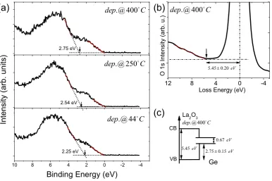
The band diagram of the La2O3/Ge stack deposited at 400C was derived using the valence81,82 and O1s energy
loss XPS spectra83,84 and is shown in Fig. 4. The high resolution valence band (VB) spectra for the three
La2O3/Ge stacks are plotted in Fig. 4(a). Although the accuracy in the determination of the Ge VB maximum is
quite limited, we measure a VBO value of 2.75 0.15 eV for 400C deposited sample, in reasonable agreement
with the theoretically predicted value of 3.0 eV for La2GeO5 and La2Ge2O7 compounds57. The band gap is
usually obtained from the inelastic energy loss features observed on the high binding energy side of the core
level photoemission peaks79,82,84. The band gap equals the energy distance between the photoemission peak
centroid and the onset of the features due to single particle excitations83. Fig. 4(b) shows the energy loss features
of the O 1s peak for the 400C deposited sample. The band gap of the LaGeOx film was determined to be 5.45
0.2 eV. By taking into account the band gap of Ge of 0.67 eV, the calculated CBO for LaGeOx/Ge is about 2 eV
(Fig. 4(c)). This is in agreement with the IPE study on ZrO2/La2O3/Ge film which indicates CBO of interfacial
LaGeOx film of > 2.0 eV50. It is worth noting that the valence band edge of La2O3 films reduces by about 0.5 eV
as the deposition temperature decreases from 400C to 44C as can be seen from Fig. 4(a). This observation
might indicate structurally different multi-layer stacks; in particular for the 44C sample, where the MEIS
results point to predominantly La2O3 layer on top. For the latter, this implies a VBO of 2.25 0.15 eV and
hence conduction band offset value for La2O3 on Ge of ~ 2.6 eV from our work, in close agreement with
theoretically predicted CBO value of 2.56 eV52,53. It has been observed that La2O3 reacts strongly with Ge
substrate to form spontaneously a nearly uniform LaGeOx compound across the entire film thickness during
deposition47-49. It is evident from the XPS Ge 3d core level spectra in Fig. 2 that LaGeOx is indeed formed at all
deposition temperatures in this study. However, our results do not show a uniform layer across the whole
thickness of the gate stack. This is particularly evident at lower temperatures. Furthermore, the noticeable shift
in the valence band offset in Fig. 4(a) cannot be explained by the formation of a structurally different germanate
layer formed at a different deposition temperature. Theoretical work points to the band gap and band offsets of
the La germinates to be relatively independent of Ge content, because the valence band top is formed of O 2p
states and the conduction band bottom is formed of La 4d states, which do not change with composition51. The
theoretically predicted values of band gap and valence band offsets are 5.0 eV and 3.0 eV respectively for both
La2Ge2O7 and La2GeO551. However, the observed band line-up substantiates the structural observation from
MEIS on transition from a bi-layer La2O3/LaGeOx at 44C to predominantly LaGeOx/Ge gate stack at 400C. A
further argument which underpins our band line-up results, is the observation from electrical measurements44
that the stack with the best passivation efficiency, that is the lowest Dit < 91011 eV-1cm-2, has been obtained at
the highest deposition temperature (360C); however with higher leakage current and lower scalability in
8
for as-deposited La2O3/Ge stacks has been reported to be < 91011, 1.41012, 31012 and 41012 for samples
deposited at 360°C, 225°C, 150°C and room temperature (44°C) respectively44.
In summary of this section, our structural study on MBE-deposited La2O3/Ge gate stacks shows that as the
deposition temperature increases, the stack converts towards a uniform LaGeOx layer which is beneficial for
passivation of the Ge surface. However, the conduction band offset drops by ~ 0.5 eV causing higher leakage,
leads to a permittivity reduction to ~ 1244 and hence lowers the scalability. Moreover, our study confirms that
La2O3 reacts strongly with Ge and removes the GeO2 completely. This could allow an abrupt LaGeOx/Ge
interface, introducing remote phonon and Coulombic scattering centers directly on the channel and so reducing
carrier mobility57.
B. Y2O3/Ge and Al2O3/Ge gate stacks
This section presents a detailed VUV-VASE study of Y2O3/Ge stacks deposited at two different temperatures
(225C and 400C) with a special emphasis on determining the dielectric function and absorption coefficient
spectra, as well as estimating the band gap and sub-band gap absorption features. The interfacial composition,
band line-up and crystallinity were ascertained from XPS and XRD measurements. In addition, the effect of
Al2O3 as a capping layer was studied.
B.1. Thickness, band gap and sub-band gap absorption
Spectroscopic ellipsometry is very sensitive to the presence of surface layers in the order of just a fraction of a
nanometer. The primary sensitivity comes from changes in phase, i.e. ellipsometric angle . Due to the high
energy range of SE measurements in this study, all dielectric films became absorbing. The UV absorption is
often modelled using a Tauc-Lorentz dispersion relationship85. The overall absorption shape is described by an
amplitude, broadening, center energy, and band gap energy. The index of refraction is determined from both the
Kramers-Kronig (KK)86 transformation of imaginary part of dielectric function along with addition of an offset
and UV pole to account for absorption that is outside the measurement spectral range. The modelling and fitting
procedure in this study consisted of firstly, determining the thickness and optical constants in non-absorbing
(transparent) region of spectra from 0.5–6 eV using a Cauchy layer representative of a dielectric film. Then, a
Kramers-Kronig consistent B-spline layer87 was used to extend the optical constants into the higher energy
range, up to 8.5 eV. This method is consistent with the point-by-point fit method88 used in WVASE32, but with
two added advantages: firstly the layer maintains KK consistency which forces the optical constants to keep a
physical shape, secondly the optical constants remain smooth and continuous over the full spectrum, with a
controllable parameter to decide the resolution of points. Additionally, the B-spline layer was replaced with the
general oscillator model with a possibility of using Cody-Lorentz and Tauc-Lorentz oscillators to discern
possible sub-band gap absorption features in the gate stacks and to determine the band gap.
Optical constants for germanium are available in the literature up to 6 eV photon energy range. We used this
9
measurements (upon opening the container in N2 purged environment) on a Ge substrate gave a GeO2 native
oxide thickness of 2.93 nm. Then the germanium optical constants were fitted using a Kramers-Kronig
consistent B-spline layer over the entire spectral range. This sample was used as a reference Ge substrate layer
to determine the optical constants of thermally grown GeO2 as well as Y2O3 and Al2O3 films. The thickness
values of the stacks are summarized in Table I. It can be seen that the thickness of Y2O3 films is ~ 6-8 nm, and
of Al2O3 ~ 8-9 nm. The reference thermally grown GeO2 layers have thicknesses of 4.4 nm (non-capped) and
3.2 and 7.2 nm for Al2O3 capped samples. The mean squared error between the experimental and theoretical
curves was in all cases below 5, consistent with a good quality fit of the data.
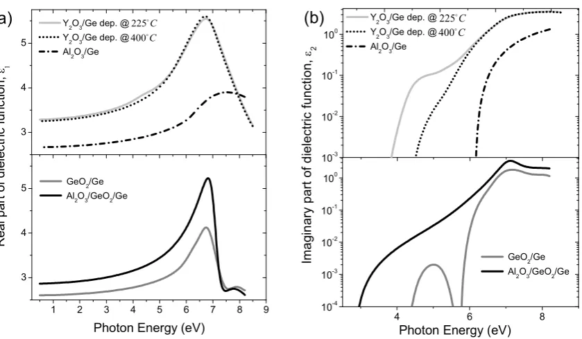
The real and imaginary part of dielectric function vs photon energy (E) for the stacks is shown in Figs. 5(a) and
(b) respectively. A pronounced absorption below the band edge can be observed for the Y2O3/Ge sample
deposited at 225C, and this is visible in the energy range from about 4 to 5.5 eV in both real and imaginary
parts of the dielectric function spectra (see top graphs in Figs. 5(a) and (b)). The band-edge tailing is much less
apparent for the Y2O3/Ge deposited at higher temperature of 400C. For comparison of these spectra, in the
bottom parts of Figs. 5(a) and (b), the real (1) and imaginary (2) parts of dielectric function for GeO2/Ge
samples, both non-capped and Al2O3 capped, are plotted as a reference. The sub-band gap features are evident
for GeO2/Ge samples and this region correlates with the pronounced absorption for the Y2O3/Ge sample
deposited at 225C. For the reference GeO2/Ge sample in this work, a peak appears at ~ 5 eV, while in Ref. 39,
two peaks are visible, at 4.4 eV (due to Ge) and at 5.1 eV. Toriumi et al.89 have reported a peak at 5.1 eV for the
GeO2/Ge sample, thought to be associated with neutral O vacancies or Ge+2 in oxygen deficient GeO290. The
high-level ab-initio calculations91,92 have shown that –GeX3 (E center @ 5.06 eV90) and X3Ge-GeX2 (E-oxygen
vacancy @ 5.16 eV90) defects are able to form a broad absorption band near 5 eV. Note that X refers to –OH
and -OGeH3 simulating the :Ge< defect92. From the data in Fig. 5(b) it is evident that the pronounced sub-band
gap absorption for Y2O3/Ge sample deposited at 225C compares to the absorption features in the GeO2/Ge
spectra and could indicate a possible defective non-stoichiometric germanium oxide interfacial layer. Such an
interfacial layer is not apparent for the sample deposited at 400C.
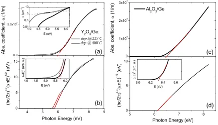
Following the extraction of the dielectric function ( ) for the Y2O3, Al2O3 and GeO2 films using
the methodology above, the 1 and 2 parameters are converted into refractive index (n) and extinction
coefficient (k) using the KK relations. The absorption coefficient () can be found from the extinction
coefficient as
hc
E
E
k
(
)
4
(1)where h is the Planck’s constant, c is the speed of light and E is the photon energy. The band gap in this work is
extracted from the Tauc-Lorentz model85 and -method. The functional form of the Tauc-Lorentz model and its
simplified expression93,94 are given in the Appendix. The plots of vs E for Y2O3 and Al2O3 films are shown in
Figs. 6(a) and (c) respectively. The associated Tauc-Lorentz plots are depicted in Figs. 6(b) and (d). The linear
2 1 ~
10
extrapolation of the segments on the curves in the non-absorbing regions gives the band gap values of 5.99 eV
for Y2O3 layers, and 6.43 eV for Al2O3 layer from -method. The associated band gap values from the
Tauc-Lorentz plots are ~ 0.3 eV lower than those derived from the -method. This result is in agreement with the
observations in Ref. 95 that the band gap values obtained from the -method can be by ~ 0.7 eV larger than the
ones determined using the Tauc- or Cody-Lorentz methods (see Appendix). In the insets of Figs. 6(b) and (d),
the corresponding (E)2 vs E graphs are added (valid for direct band gap transitions96). A summary of the
experimental band gap data obtained from this work and literature39,56,66,97-102 is shown in Table I. It can be seen
that the band gap of Y2O3 from the Tauc plots is 5.7 0.1 eV for both deposition temperatures. A similar value
has been reported for a radio frequency (rf) sputtered Y2O3/Ge stack using SE56 and XPS66 measurements. The
value reported for Y2O3 on Si is 5.6 (from SE)97, on SiO2 is 6.0 (from XPS)98, and for single crystal 6.1 eV
(from SE)99.
The Tauc coefficient is found to be 1145.4 eV-1/2cm-1/2 for both samples. It has been argued that the Tauc plot is
related to the degree of order in the structure103, i.e. disorder generates defects and hence removes states from
the bands and generates band tails of localized states. These band tails are generally described by the Urbach
exponential104
, (2)
where 0 is the constant and Eu is the Urbach energy. In a logarithmic plot of the absorption coefficient, the
Urbach tail appears as a linear region at energies below the absorption edge. The logarithmic plot of vs E, in
the sub-band gap energy range (< 6 eV) is shown in the inset of Fig. 6(a). An apparent linear region of the plot
is visible for the Y2O3 sample deposited at 225C, being indicative of a presence of an Urbach tail. The inverse
of this slope gives the Urbach energy of 1.1 eV. The values of Eu = 1.4 eV and the Tauc coefficient of 1344 eV -1/2
cm-1/2 have been reported for polycrystalline HfO2 film103. A decrease in band tailing for the HfO2 samples
annealed at higher temperatures has been reported and attributed to defect reduction and temperature induced
crystallization105,106. The amorphous samples have been proposed to have a continuous and more dense bond
network and hence a lower density of defects, which is substantiated by the lower trapped charge density103,107.
In this work, the sample deposited at higher temperature shows no apparent Urbach tail and has less pronounced
sub-band gap absorption region. However, there is no shift of the band edge in comparison to 225C deposited
sample (see Fig. 6(a)), indicating a similar structure. This argument is substantiated by the XRD graphs shown
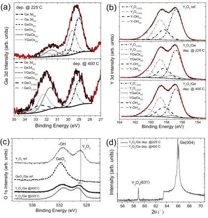
in Fig. 7(d), where both films prove to be polycrystalline. The XRD pattern shows polycrystalline phases of Ge
(004) plane and Y2O3 (631) plane for both samples.
B.2. Interfacial layer study for Y2O3/Ge
The Ge 3d XPS core levels can best represent the chemistry at the interface because of their sufficient surface
sensitivity and good resolution due to a narrow FWHM108. The relevant Ge 3d spectra fitted using a doublet
)
exp(
0
u
E
E
11
(due to spin-orbit splitting) Voigt functions for each peak are shown in Fig. 7(a). The Ge 3d0 substrate peak is
fitted with a doublet of Ge 3d5/2 (@29.0 eV) and Ge 3d3/2 (@ 29.6 eV) with spin-orbit splitting of 0.6 eV and
intensity ratio of 2:3 respectively. A high BE shoulder to the Ge 3d0 substrate peak can be seen for both Y2O3
samples, however with a higher intensity for the layer deposited at 400C (see Fig. 7(a) bottom). Also note that
Ge 3d0 is less pronounced for the latter due to the thicker dielectric layer for this sample (see Table I, 7.9 nm for
400C vs 6.3 nm for 225C deposited sample). The rising edge at a BE lower than ~ 28 eV originates from Y 4p
to O 2s peaks at ~ 25 eV. The formation of the interfacial layer will be reflected in the Ge 3d spectra as positive
shifts (with respect to the substrate Ge 3d0 peak) when Ge reacts to form YGeOx layer. It has been reported that
the Y-Ge-O bonding configuration gives rise to a BE shift within the range of + 2.2 to 2.5 eV due to a second
nearest-neighbor effect, which is distinctly different from a O-Ge-O type bonding (+3.4 eV shift)77,109. In our
spectra in Fig. 7(a), the chemical shift for YGeOx layer is visible at +2.5 to + 2.7 eV from the substrate peak.
Note the difference in the interfacial layer between the two samples. The lower temperature deposited Y2O3/Ge
stack features GeOx layer at the interface, with a chemical shift of 1.1 eV consistent with +1 Ge oxidation
state78. The higher temperature deposited stack has sub-oxide fully eliminated, and GeO2 appears at the
interface.
The Y 3d core level spectra were also measured to study the additional bonding and are shown in Fig. 7(b). The
peak appearing at ~156.95 eV for Y2O3/Ge samples represents the co-existence of Y2O3 at 156.86 eV (see top
graph for Y2O3 reference in Fig. 7(b)) and Ge–O–Y bonding at 157.28 eV (see middle and bottom part of Fig.
7(b)). In addition, a positive shift from a reference Y2O3 bulk value can be seen from the O 1s spectra shown in
Fig. 7(c), and this provides firm evidence of charge transfer and formation of YGeOx at the interface. Note also
that both the Y 3d and O 1s spectra show that Y-OH bond from moisture absorption is present, as in the case of
La2O3/Ge stacks.
The results imply that Y–O–Y bonding configuration near the surface transforms to a Y–O–Ge configuration
near the interface due to the incorporation of Ge atoms into the Y2O3 matrix. It has been inferred that Y and Ge
atoms intermix more significantly at a higher process temperature68. The out-diffusion of Ge signifies the
breaking of the strong covalent Ge-Ge bonds even at room temperature. The chemical bonding model proposes
possible bond weakening via charge transfer during the formation of chemical bonds110. Since the electronegativity difference between Y and Ge (1.22 and 2.01 using Pauling’s scale) is large, charge transfer and
hence the bond weakening can be significant. Room temperature mixing has also been observed for Si, and the
concept of metallic screening of covalent bonds has been used to explain the bond weakening111,112.
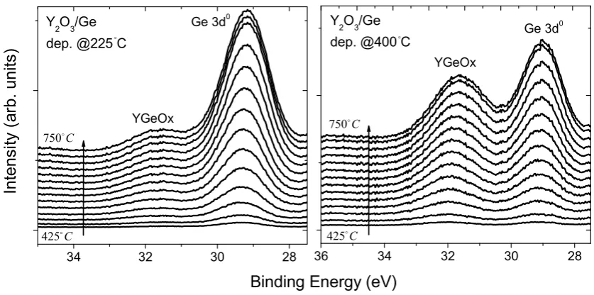
In order to study the effect of temperature on the interfacial layer characteristics of Y2O3/Ge, XPS in-situ
annealing measurements were performed in the temperature range of 425°C to 750°C, with a step of 25°C. The
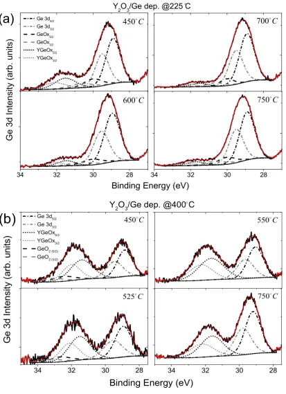
Ge 3d core level spectra as a function of annealing temperature are shown in Fig. 8. A stronger formation and
more pronounced YGeOx shoulder is visible for the Y2O3/Ge sample deposited at 400°C. The fitting of the Ge
3d core level at different annealing temperature is performed using the same procedure described above. The
relevant graphs for the two Y2O3/Ge samples are shown in Figs. 9(a) and (b). The Y2O3 sample deposited at
12
be seen from Fig. 9(a). On the contrary, the 400°C deposited Y2O3 sample shows presence of GeO2 IL layer
until the annealing temperature of 525°C. For this gate stack after the 550°C annealing temperature, the
interface is pristine YGeOx layer.
B.3. Estimation of VBO and derivation of a band diagram for Y2O3/Ge
According to Kraut’s method113
, the valence band offset value for a Y2O3/Ge heterojunction can be determined
using the following equation
(3)
where EGe3d and EY3d are the binding energies of the Ge 3d and Y 3d core levels that have been selected as
references for Ge substrate and Y2O3 respectively. Ev refers to the valence band maximum (VBM) for the Ge
substrate and bulk reference Y2O3 sample and can be estimated from the valence band spectra using linear
interpolation method114. The term CL is defined as the energy difference between the Ge 3d and Y 3d core
levels referring to Ge substrate and Y2O3 from the interface Y2O3/Ge sample, i.e.
.
Fig. 10(a) shows the selected core levels and valence band spectra for a clean bare n-Ge substrate (top), for
interfacial Y2O3/Ge (middle) and for a bulk Y2O3 (bottom) films. The energy difference between the Ge 3d 5/2
and the VBM in the bare, pre-clean Ge sample (Fig. 10(a), top) was measured to be 29.41 0.1 eV. This value
compares to published results of 29.47 0.07 eV115, 29.40 0.03 eV116, 29.30 0.1 eV117, and 29.61 0.1 eV39.
The value of CL is found to be 127.77 0.1 eV for the Y2O3/Ge deposited at 225°C (shown in Fig. 10(a),
middle), and 127.85 0.1 eV for the sample deposited at 400°C. The energy difference for the bulk Y2O3
reference sample was estimated to be 154.50 0.1 eV. By inserting the estimated values in Eq. (3), the VBO is
determined to be 2.68 0.2 eV. The valence band spectra for the two Y2O3/Ge stacks are depicted in Fig. 10(b).
We measure directly from these graphs VBO values of 2.45 eV and 2.34 eV with an error bar of 0.2 eV, for
225°C and 400°C deposited samples respectively. It is worth noting that the VBO value is within the tolerance
bar of the measurement for both samples. This is in contrast with the La2O3/Ge samples, where a more
substantial decrease of the VBO value with the raise of the deposition temperature was observed (see Fig. 4(a)).
Note that the spectra shown in Fig. 4(a) are obtained from an instrument with higher spectral resolution than
once shown in Fig. 10(b). It is worth mentioning that we have re-measured the core levels (Ge 3d, Y 3d, O 1s)
and valence band region for the Y2O3/Ge samples using a monochromated XPS instrument, and the result of
2.68 0.2 eV was confirmed using the Kraut method. The full band diagram of Y2O3/Ge is drawn in Fig. 10(c)
using the Kraut’s value of the VBO and the band gap value obtained from the Tauc plots (see section B.1). The
conduction band offset (CBO) for Y2O3/Ge stack is calculated to be 2.35 eV. The value of the VBO of 2.78 eV
has been reported for Y2O3/Ge from the Kraut’s method in Ref. 66, however the values of the core level
VBO
=
(
E
Ge3d-
E
V)
Ge
-(
E
Y3d-
E
V)
Y2O3
+
d
CL
d
CL=
E
Ge3d Ge-
E
13
differences in Eq. (3) have not been stated, so direct comparison with our data is not possible. The obtained
CBO value of 2.35 eV from this work compares to the theoretically predicted value of 2.56 eV52,53.
B.4. Electrical characterization of Y2O3/Ge stacks
The high frequency capacitance voltage and leakage current density characteristics for a MIS capacitor from the
as-deposited Y2O3 films grown at 225C and 400C, are shown in Figs. 11 and 12, respectively. The CV curves
of the 225C deposited Y2O3 sample (Fig. 11(a)) exhibit high frequency dispersion with large bumps in the
weak inversion regime. A notable improvement in the CV characteristics is observed as the growth temperature
increases from 225C to 400C. The aforementioned result could be correlated with the Ge 3d XPS spectra
presented in Fig. 7, where full elimination of GeOx sub-oxide and enhanced YGeOx formation have been
demonstrated in the case of the 400C-deposited Y2O3/Ge stack.
It is evident from Fig. 12 that the leakage current of the 400C-deposited sample is subsequently kept below 10-6
A/cm2 at 1 V, as opposed to La2O3 that suffers from high leakage current of ~ 10-1 A/cm2 at 1 V for samples
deposited at 360C (see Ref. 44). This observation is in good agreement with the band diagrams presented in
Figs. 4 and 10, where the Y2O3/Ge stack was found to exhibit a higher conduction band offset (> 2.3 eV), than
the respective La2O3/Ge (~ 2 eV). Furthermore, this behaviour is in good agreement with the reported VASE
and XPS spectra of the as-deposited Ge/Y2O3 samples (see Figs. 5, 7(a) and 9), where a reduction of defective
GeOx species has been observed at a growth temperature of 400C.
C. The effect of an Al2O3 capping layer
The band gap value of Al2O3 layer is found to be 6.1-6.4 from the VUV-VASE results (see Table I and Fig.
6(c)-(d)). The ALD-deposited Al2O3 has been reported to have a much lower density (3.1-3.3 g/cm3) than
sapphire, and a lower band gap of ~ 6.2 eV (from photoconductivity measurements)100,101 and 6.5 eV (from
XPS)102; for sapphire the band gap is 8.8 eV53,118. No Urbach tail was evident for the Al2O3/Ge in this work,
suggesting a negligible sub-band gap absorption. It has been argued recently that Al2O3 is a good oxygen
diffusion barrier and therefore blocks the O vacancy diffusion that allows the volatilisation of GeO and the
creation of sub-stoichiometric GeOx interface states57. Calculations of electronic structures of interfaces and
interface defects and of oxide reactions and considerations of diffusion barrier properties by Robertson’s group57,119 suggest that a thin Al2O3 layer in the overall dielectric might be a preferred passivation scheme for
Ge channels34,35. Furthermore, the difference in the O density between La2O3, Y2O3 and Al2O3 allows for
different behaviour of these oxides on Ge49. As discussed in the introduction, both La2O3 and Y2O3 belong to a
group of intimate dielectrics on Ge, i.e. they form stable germanate layers in contact with Ge. On the contrary,
Al2O3 acts as a barrier on Ge. This has further been associated with the cation radius of the corresponding
oxides49. In particular the large ionic radius of La+3 (117 pm) compared to Al+3 (67.5 pm), implies large M–O
14
The interfacial features for the selection of GeO2/Ge with and without Al2O3 capping layers can be found from
inspecting the Ge 3d core levels, and are shown in Fig. 13. For the non-capped 4.4 nm GeO2/Ge layer, a strong
presence of Ge+4 oxidation state is evident from the chemical shift to the Ge 3d0 peak of > 3 eV49,77-78 (Fig.
13(a)). After the Al2O3 capping layer deposition on 3.2 nm GeO2/Ge, the shift to lower binding energy of the IL
peak in Fig. 13(b) reveals the impact of Al2O3 deposition on the GeO2 layer. This behaviour suggests the
formation of a germanate layer (AlGeOx) at the Al2O3/GeO2 interface. Note also the presence of GeOx at the
interface for this sample. For the thicker 7.2 nm GeO2 layer with Al2O3 cap, only a sub-peak referring to
AlGeOx can be observed from Fig. 13(c). In the case of Al2O3/Ge, no high BE shoulder is apparent, rather just a
peak referring to the Ge 3d0 substrate (Fig. 13(d)) suggesting no IL. Further evidence comes from the Al 2p
spectra shown in Fig. 14. The Al 2pspectrum for Al2O3/Ge sample exhibits no clear change, suggesting that
there is no detectable chemical reaction in the Al2O3 capping layer, and that Al2O3 acts indeed as a barrier layer.
On the contrary, for the Al2O3/GeO2/Ge structures there is a clear shift for both Al 2p and O 1s peaks towards
higher BEs in agreement with AlGeOx formation discussed above. These observations indicate that the Ge
in-diffusion through the GeO2 into the Al2O3 and the intermixing between these different layers lead to a AlGeOx
IL formation, possibly more stable than the GeO2 interlayer29. A recent theoretical study predicted that the
incorporation of Al into the GeO2 matrix leads only to the formation of Ge–O–Al bonds, with no defect states
inside the Ge bandgap19, indicating that the formation of the AlGeOxinterlayer should not be detrimental to the
interface quality7,22,34,35.
In summary of this section, there is evidence that Y2O3 shows a more moderate reactivity to Ge and shows
feasibility for a GeO2-interfacial layer at the higher deposition temperature of 400C. The conduction band
offset has been derived from the XPS and VUV-VASE data and shows a sufficiently large (~ 2.3 eV) value to
allow for the measured low leakage (< 10-6 A/cm2 @ 1 V). The stack transforms into pristine YGeOx/Ge layer,
with no GeO2 IL, for annealing temperature above 525C. Our experimental results confirm that Al2O3 acts as a
barrier on Ge, with no detectable IL, within a resolution of the experimental techniques used.
IV. SUMMARY & OUTLOOK
A comprehensive study of ultra-thin La2O3/Ge and Y2O3/Ge gate stacks prepared by molecular beam epitaxy
has been conducted in this paper for consideration as interfacial layers for Ge surface passivation. In particular,
the effect of deposition temperature, ranging from 44-400C, on interfacial features, band line-up, band gap and
sub-band gap absorption, and crystallinity has been investigated by MEIS, VUV-VASE, XPS and XRD
techniques. Both La2O3 and Y2O3 show a reactivity to germanium. A strong presence of germanate layers was
found from the high binding energy shoulders to the Ge 3d substrate XPS core level peak, with a chemical shifts
of +2.5-2.6 eV for LaGeOx, and +2.5-2.7 eV for YGeOx. The higher deposition temperature the higher intensity
of the germanate layers formation was evident for both gate stacks. However, the interface structure was found
to be somewhat different. In the case of La2O3/Ge, there is no GeO2 present at the interface for all deposition
temperatures studied, rather germanium sub-oxide species dominate the interface and even they have been found
in the bulk of ultra-thin (2-3 nm) films from angle-resolved XPS data. The high-resolution valence band spectra
15
deposition temperature increased from 44C to 400C. This observation underpins previously reported electrical
characterization data that the stack with the best passivation efficiency has a uniform LaGeOx layer, but with
higher leakage current and hence low scalability. The band diagram has been derived for LaGeOx/Ge from the
XPS data with values for valence band offset of 2.75 0.15 eV and band gap of 5.45 0.2 eV, in reasonable
agreement with recent theoretical calculations.
A Y2O3/Ge gate stack deposited at 225C shows a GeOx interfacial layer. The VUV-VASE data have enabled
extraction of dielectric function and absorption coefficient versus photon energy for the Y2O3/Ge stacks. The
pronounced sub-band gap absorption region is distinctly evident in the broad region from ~ 4.5-5.5 eV from the
imaginary part of dielectric function and absorption coefficient spectra for the 225C deposited stack. This
absorption range could be attributed to a reported neutral oxygen vacancy coordinated with two Ge ions (at 5.06
eV) and/or a Ge+2 coordinated with two oxygens (at 5.16 eV) defects; this result substantiates the existence of
sub-stoichiometric GeOx layer. The stack deposited at 400C has no such absorption region, and GeO2
interfacial layer has been found from the Ge 3d XPS core level spectra. Furthermore, after the annealing above
525C, this stack has become GeO2-free, transforming into pristine YGeOx/Ge layer. The band diagram has
been derived for the Y2O3/Ge using the Kraut’s method for the estimation of VBO (2.68 0.2 eV) and
Tauc-Lorentz method for the band gap (5.7 0.1 eV). The band gap of Al2O3 has been found to be 6.1-6.4 eV from
the Tauc-Lorentz and -methods. There was no detectable interfacial layer for Al2O3/Ge stack, indicating
possible barrier role of alumina layer.
A notable improvement in the capacitance voltage and leakage current density characteristics has been observed
for the Y2O3/Ge stacks as the growth temperature increased from 225C to 400C. This result is in agreement
with the structural data, as the detrimental effect of GeOx interfacial layer on electrical properties can be
expected for the 225C deposited stack.
In summary, the results of this study unambiguously point to two important findings: firstly the optimal
deposition temperature is in the higher range, at ~ 400C, as this allows for more uniform germanate layer at the
interface with better passivation properties; secondly comparing two rare-earth stacks, La2O3/Ge with Y2O3/Ge,
deposited at the optimal temperature (~ 400C), the latter is seen to have more attractive features for Ge
interface engineering: moderate reactivity to Ge, GeOx-free interface, higher conduction band offset (~ 2.3 eV),
larger band gap (~ 5.7 eV), and lower leakage current (< 10-6 A/cm2 at 1 V). As such, Y2O3/Ge is a serious
contender for interface engineering in future Ge CMOS technology.
ACKNOWLEDGEMENTS
The work was funded by the EPSRC grant no. EP/1012907/1, United Kingdom. The MEIS measurements were
performed courtesy of Dr P. Bailey and Dr T.C.Q. Noakes from the Daresbury Laboratory, UK. The
VUV-VASE experiments were done at J.A. Woollam Co. Inc., NE, USA courtesy of J.N. Hilfiker. The authors thank
16
Department at the University of Manchester, UK for XRD measurements, and Prof C. McConville at University
of Warwick, UK for use of monochromated XPS system. One of the authors (MA) acknowledges support from
Physics Department, Taif University, Saudi Arabia. Also thanks to P. Spencer from Physics Department,
University of Liverpool, UK for performing some of the XPS experiments in this work under the EPSRC 2011
vacation bursary award scheme.
APPENDIX
The band gap can be determined from the spectroscopic ellipsometry data using a linear extrapolation of the
threshold of optical absorption from either the extinction coefficient (k) curve, the imaginary part of the
dielectric function (2) , the absorption coefficient () curve, or plots of the Tauc-Lorentz and Cody-Lorentz95. It
has been shown95 that the band gap value determined from the -method is larger than those determined from
the k and 2 methods, due to an extra factor of energy gained when converting from k or 2 to . This factor of
energy adds an additional concave upwards nature to the absorption coefficient curve, which has the effect of
shifting the linearly extrapolated band gap to higher energy. On the contrary, the Tauc and Cody-Lorentz
generate smaller band gap values due to the fact that it uses the square root of the imaginary part of the
dielectric function, which decreases the concave upwards nature of the spectrum.
The functional form of the Tauc-Lorentz model85 is given as
, (A.1)
where A is the transition amplitude, C is the broadening coefficient of the Lorentz oscillator, E0 is the peak
position for the Lorentz oscillator, E is the photon energy, and Eg is the band gap energy defined as the photon
energy where 2 = 0. Note that this formula is valid only for photon energies greater than the band gap energy.
The Eq. (A.1) can be simplified by taking into consideration that 2 is proportional to (E-Eg)2/E2, hence it can be
re-written93,94 as
(A.2)
where h is the Planck’s constant, c is the speed of light, and n – refractive index. Then from Eq. (A.2), plotting
(hc/2)1/2(nE)1/2 versus photon energy (E) allows for the straightforward linear extrapolation of the band gap
from the graph.
2 2 2 2 0 2 2 0 2 2 2 2 0 2 0 2 2 2
)
(
)
(
1
)
(
)
(
)
(
E
C
E
E
E
E
C
AE
E
E
C
E
E
CE
E
A
E
E
E
A
E
g L g T
E
E
n
E
hc
E
E
E
E
g(
)
(
)
2
)
(
22
17
REFERENCES
1
S. Takagi, R. Zhang, and M. Takenaka, Microelectron. Eng. 109, 389 (2013).
2
A. Toriumi, C.H. Lee, S.K. Wang, T. Tabata, M. Yoshida, D.D. Zhao, T. Nishimura, K. Kita, K. Nagashio,
Proc. IEEE IEDM Tech. Dig. 2011, 646.
3
M. Caymax, G. Eneman, F. Bellenger, C. Merckling, A. Delabie, G. Wang, R. Loo, E. Simoen, J. Mitard, B.
De Jaeger, G. Hellings, K. De Meyer, M. Meuris, and M. Heyns, Proc. IEEE IEDM Tech. Dig. 2009, 461.
4
P.C. McIntyre, D. Chi, C.O. Chui, H. Kim, K.I. Seo, K.C. Saraswat, R. Sreenivasan, T. Sugawara, F.S.
Aguirre-Testado, and R.M. Wallace, ECS Trans. 3,519 (2006).
5
M. Caymax, S. Van Elshocht, M. Houssa, A. Delabie, T. Conard, M. Meuris, M.M. Heyns, A. Dimoulas, S.
Spiga, M. Fanciulli, J.W. Seo, and L.V. Goncharova, Mater. Sci. Eng.B 135,256 (2006).
6
A. Toriumi, T. Tabata, C.H. Lee, T. Nishimura, K. Kita, and K. Nagashio, Microelectron. Eng. 86,1571
(2009).
7
Q. Xie, S. Deng, M. Schaekers, D. Lin, M. Caymax, A. Delabie, X-P. Qu, Y-L. Jiang, D. Deduytsche, and C.
Detavernier, Semicond. Sci. Techn. 27, 074012 (2012).
8
T. Nishimura, C.H. Lee, S.K. Wang, T. Tabata, K. Kita, K. Nagashio, and A. Toriumi, Proc. IEEE Symp. on
VLSI Techn. 2010, 209.
9
C.H. Lee, T. Nishimura, T. Tabata, S.K. Wang, K. Nagashio, K. Kita, and A. Toriumi, Proc. IEEE IEDM
Tech. Dig. 2010, 416.
10
C.H. Lee, T. Nishimura, N. Saido, K. Nagashio, K. Kita, and A. Toriumi, Proc. IEEE IEDM Tech. Dig. 2009,
457.
11
C.H. Lee, T. Nishimura, K. Nagashio, K. Kita, A. Toriumi, IEEE Trans. Electron. Dev. 58(5), 1295 (2011).
12
A. Delabie, F. Bellenger, M. Houssa, T. Conard, S. V. Elshocht, M. Caymax, M. Heyns, and M. Meuris,
Appl. Phys. Lett. 91, 082904 (2007).
13
H. Matsubara, T. Sasada, M. Takenaka, and S. Takagi, Appl. Phys. Lett. 93, 032104 (2008).
14
Y. Nakakita, R. Nakane, T. Sasada, H. Matsubara, M. Takenaka, and S. Takagi, Proc. IEEE IEDM Tech. Dig.
2008, 877.
15
R. Xie, T. H. Phung, W. He, Z. Sun, M. Yu, Z. Cheng, and C. Zhu, Proc. IEEE IEDM Tech. Dig. 2008, 393.
16
H.-Y. Yu, M. Ishibashi, J.-H. Park, M. Kobayashi, and K. C. Saraswat, IEEE Electron Device Letters 30, 675
(2009).
17
A. Molle, N.K. Bhuiyan, G. Tallarida, and M. Fanciulli, Appl. Phys. Lett. 89(8), 083504 (2006).
18
D. Kuzum, P. Jin-Hong, T. Krishnamohan, H-S.P. Wong, K.C. Saraswat, IEEE Trans. Electron. Dev. 58(4),
1015 (2011).
19
M. Houssa, G. Pourtois, M. Caymax, M. Meuris, and M. M. Heyns, Appl. Phys. Lett. 92(24), 242101 (2008).
20
K. Prabhakaran, F. Maeda, Y. Watanabe, and T. Ogino, Appl. Phys. Lett. 76(16), 2244 (2000).
21
T. Takahashi, T. Nishimura, L. Chen, S. Sakata, K. Kita and A. Toriumi, Proc. IEEE IEDM Tech. Dig. 2007,
697.
22
C.H. Lee, T. Tabata, T. Nishimura, K. Nagashio, and A. Toriumi, Appl. Phys. Express 2, 071404 (2009).
23
18 24
F. Bellenger,B. De Jaeger, C. Merckling, M. Houssa, J. Penaud, L. Nyns, E. Vrancken, M. Caymax, M.
Meuris, T. Hoffmann, K. De Meyer, and M. Heyns, IEEE Electron Device Lett.31(5),402 (2010).
25
Q. Xie, D. Deduytsche, M. Schaekers, M. Caymax, A. Delabie, X.P. Qu, and C. Detavernier, Electrochem.
Solid State Lett.14,G20 (2011).
26
Y. Fukuda, Y. Yazaki, Y. Otani, T. Sato, H. Toyota, and T. Ono, IEEE Trans. Electron Devices 57, 282
(2010).
27
K. Kita, S.K. Wang, M. Yoshida, C.H. Lee, K. Nagashio, T. Nishimura, and A. Toriumi, Proc. IEEE IEDM
Tech. Dig. 2009, 693.
28
R.D. Shannon, J. Appl. Phys. 73, 348 (1993).
29
A. Dimoulas, D.P. Brunco, S. Ferrari, J.W. Seo, Y. Panayiotaos, A. Sotiropoulos, T. Conard, M. Caymax, S.
Spiga, M. Fanciulli, Ch. Dieker, E.K. Evangelou, S. Galata, M. Houssa, and M.M. Heyns, Thin Solid Films 515,
6337 (2007).
30
T. Tabata, C. H. Lee, K. Kita and A. Toriumi, ECS Trans. 16(5), 479 (2008).
31
J.J. Gu, Y.Q. Liu, M. Xu, G.K. Celler, R.G. Gordon, P.D. Ye, Appl. Phys. Lett. 97, 012106 (2010).
32
K. Kita, K. Kyuno, and A. Toriumi, Appl. Phys. Lett. 85, 52 (2004).
33
R. Zhang, T. Iwasaki, N. Taoka, M. Takenaka, and S. Takagi, Proc. IEEE Symp. VLSI Techn. 2011, 56.
34
R. Zhang, P.C. Huang, J.C. Lin, M. Takenaka, and S. Takagi, Proc. IEEE IEDM Tech. Dig. 2012, 371.
35
R. Zhang, T. Iwasaki, N. Taoka, M. Takenaka, S. Takagi, IEEE Trans. Electron Dev. 59, 335 (2012).
36
R. Zhang, T. Iwasaki, N. Taoka, M. Takenaka, and S. Takagi, Appl. Phys. Lett. 98, 112902 (2011).
37
R. Zhang, P. C. Huang, N. Taoka, M. Takenaka and S. Takagi, Proc. IEEE Symp. VLSI Techn. 2012, 161.
38
E. Dentoni Litta, P-E. Hellström,C. Henkel, and M. Östling, IEEE Trans. Electron Dev. 60(10), 3271 (2013).
39
I.Z. Mitrovic, M. Althobaiti, A.D. Weerakkody, N. Sedghi, S. Hall, V.R. Dhanak, P.R. Chalker, C. Henkel, E.
Dentoni Litta, P.-E. Hellström, and M. Östling, Microelectron. Eng. 109, 204 (2013).
40
K. Kita, T. Takahashi, H. Nomura, S. Suzuki, T. Nishimura, and A. Toriumi, Appl. Surf. Sci. 254, 6100
(2008).
41
J. Song, K. Kakushima, P. Ahmet, K. Tsutsui, N. Sugi, T. Hattori, H. Iwai, Microelectron. Eng. 84, 2336
(2007).
42
J. Song, K. Kakushima, P. Ahmet, K. Tsutsui, N. Sugii, T. Hattori, and H. Iwai, Jap. J. Appl. Phys. 46(16),
L376 (2007).
43
G. Mavrou, S.F. Galata, A. Sotiropoulos, P. Tsipas, Y. Panayiotatos, A. Dimoulas, E.K. Evangelou, J. W.
Seo, and Ch. Dieker, Microelectron. Eng. 84, 2324 (2007).
44
G. Mavrou, S. Galata, P. Tsipas, A. Sotiropoulos, Y. Panayiotatos, A. Dimoulas, E. K. Evangelou, J. W. Seo,
and Ch. Dieker, J. Appl. Phys. 103, 014506 (2008).
45
C. Rossel, A. Dimoulas, A. Tapponnier, D. Caimi, D. J. Webb, C. Andersson, M. Sousa, C. Marchiori, H.
Siegwart, J. Fompeyrine, and R. Germann, Proc. ESSDERC 2008, 79.
46
J. Song, K. Kakushima, P. Ahmet, K. Tsutsui, N. Sugii, T. Hattori, and H. Iwai, Microelectron. Eng. 86, 1638
(2009).
47
G. Mavrou, P. Tsipas, A. Sotiropoulos, S. Galata, Y. Panayiotatos, A. Dimoulas, C. Marchiori, and J.
19 48
D. Tsoutsou, Y. Panayiotatos, A. Sotiropoulos, G. Mavrou, E. Golias, S.F. Galata, and A. Dimoulas, J. Appl.
Phys. 108, 064115 (2010).
49
A. Dimoulas, D. Tsoutsou, Y. Panayiotatos, A. Sotiropoulos, G. Mavrou, S. F. Galata, and E. Golias, Appl.
Phys. Lett. 96, 012902 (2010).
50
V. V. Afanas’ev, A. Stesmans, G. Mavrou, and A. Dimoulas, Appl. Phys. Lett. 93, 102115 (2008).
51
H. Li, L. Lin, J. Robertson, Appl. Phys. Lett. 101, 052903 (2012).
52
J. Robertson, B. Falabretti, Materials Science and Engineering B 135, 267 (2006).
53
J. Robertson, B. Falabretti, J. Appl. Phys. 100, 014111 (2006).
54
C. Andersson, C. Rossel, M. Sousa, D. J. Webb, C. Marchiori, D. Caimi, H. Siegwart, Y. Panayiotatos, A.
Dimoulas, and J. Fompeyrine, Microelectron. Eng. 86, 1635 (2009).
55
M. Leskelä and M. Ritala, J. Solid State Chem. 171(1/2), 170 (2003).
56
Y. Zhao, K. Kita, K. Kyuno, and A. Toriumi, Appl. Phys. Lett. 94, 042901 (2009).
57
H. Li, L. Lin, and J. Robertson, Appl. Phys. Lett. 101, 052903 (2012).
58
X. Zhao and D. Vanderbilt, Phys. Rev. B Condens. Matter. 65(7), 075105 (2002).
59
S. Abermann, O. Bethge, C. Henkel, and E. Bertagnolli, Appl. Phys. Lett. 94(26), 262904 (2009).
60
C. Henkel, S. Abermann, O. Bethge, G. Pozzovivo, P. Klang, M. Reiche, and E. Bertagnolli, IEEE Trans.
Electron. Dec. 57(12), 3295 (2010).
61
C. X. Li and P. T. Laia, Appl. Phys. Lett. 95, 022910 (2009).
62
Y-H. Wu, M.L. Wu, R.J. Lyu, J.R. Wu, L.L. Chen, C.C. Lin, Appl. Phys. Lett. 98, 203502 (2011).
63
Z.Q. Liu, W.K. Chim, S.Y. Chiam, J.S. Pan, C.M. Ng, Appl. Phys. Lett. 100, 092110 (2012).
64
L. K. Chu, W. C. Lee, M. L. Huang, Y. H. Chang, L. T. Tung, C. C. Chang, Y. J. Lee, J. Kwo, and M. Hong,
J. Cryst. Growth 311, 2195 (2009).
65
Z.Q. Liu, S.Y. Chiam, W.K. Chim, J.S. Pan, and C.M. Ng, J. Electrochem. Soc. 157, G250 (2010).
66
S.Y Chiam, W.K. Chim, C. Pi, A.C.H. Huan, S.J. Wang, J.S. Pan, S. Turner, J. Zhang, J. Appl. Phys. 103,
083702 (2008).
67
J. Sune, S. Tous, and E. Miranda, Appl. Phys. Lett. 97, 213503 (2010).
68
M-L. Wu, Y-H. Wu, R-J. Lyu, C-Y. Chao, C-Y. Wu, C-C. Lin, L-L. Chen, Microelectronic Eng. 109, 216-9
(2013).
69
A. Chroneos, A. Dimoulas, J. Appl. Phys. 111, 023714 (2012).
70
G. Beamson, D. Briggs, S.F. Davies, I.W. Fletcher, D.T. Clark, J. Howard, U. Gelius, B. Wannberg and P.
Balzer, Surf. Interface. Anal. 15, 541 (1990).
71
J.C. Vickerman, Surface analysis (John Wiley, 1998).
72
D.A. Shirley, Phys. Rev. B 5, 4709 (1972).
73
E. Bersch, M. Di, S. Consiglio, R.D. Clark, G.J. Leusink, A.C. Diebold, J. Appl. Phys. 107, 043702 (2010).
74
M. Perego, G. Seguini, J. Appl. Phys. 110, 053711 (2011).
75
W.F. Zhang, T. Nishimula, K. Nagashio, K. Kita, A. Toriumi, Appl. Phys. Lett. 102, 102106 (2013).
76
S. Baldovino, A. Molle, and M. Fanciulli, Appl. Phys. Lett. 93, 242105 (2008).
77
D. Schmeisser, R.D. Schnell, A. Bogen, F.J. Himpsel, D. Rieger, G. Landgren, and J.F. Morar, Surf. Sci. 172,
455 (1986).
78